EP1154511A2 - Adjusting method for electrical characteristics of microstrip line filter, duplexer, communication device, and microstrip line type resonator - Google Patents
Adjusting method for electrical characteristics of microstrip line filter, duplexer, communication device, and microstrip line type resonator Download PDFInfo
- Publication number
- EP1154511A2 EP1154511A2 EP01110330A EP01110330A EP1154511A2 EP 1154511 A2 EP1154511 A2 EP 1154511A2 EP 01110330 A EP01110330 A EP 01110330A EP 01110330 A EP01110330 A EP 01110330A EP 1154511 A2 EP1154511 A2 EP 1154511A2
- Authority
- EP
- European Patent Office
- Prior art keywords
- microstrip line
- electrode
- electrodes
- dielectric substrate
- resonator
- Prior art date
- Legal status (The legal status is an assumption and is not a legal conclusion. Google has not performed a legal analysis and makes no representation as to the accuracy of the status listed.)
- Withdrawn
Links
Images

Classifications
-
- H—ELECTRICITY
- H01—ELECTRIC ELEMENTS
- H01P—WAVEGUIDES; RESONATORS, LINES, OR OTHER DEVICES OF THE WAVEGUIDE TYPE
- H01P1/00—Auxiliary devices
- H01P1/20—Frequency-selective devices, e.g. filters
- H01P1/201—Filters for transverse electromagnetic waves
- H01P1/203—Strip line filters
-
- H—ELECTRICITY
- H01—ELECTRIC ELEMENTS
- H01P—WAVEGUIDES; RESONATORS, LINES, OR OTHER DEVICES OF THE WAVEGUIDE TYPE
- H01P1/00—Auxiliary devices
- H01P1/20—Frequency-selective devices, e.g. filters
- H01P1/201—Filters for transverse electromagnetic waves
- H01P1/203—Strip line filters
- H01P1/20327—Electromagnetic interstage coupling
- H01P1/20354—Non-comb or non-interdigital filters
- H01P1/20363—Linear resonators
-
- H—ELECTRICITY
- H01—ELECTRIC ELEMENTS
- H01P—WAVEGUIDES; RESONATORS, LINES, OR OTHER DEVICES OF THE WAVEGUIDE TYPE
- H01P1/00—Auxiliary devices
- H01P1/20—Frequency-selective devices, e.g. filters
- H01P1/213—Frequency-selective devices, e.g. filters combining or separating two or more different frequencies
- H01P1/2135—Frequency-selective devices, e.g. filters combining or separating two or more different frequencies using strip line filters
-
- H—ELECTRICITY
- H01—ELECTRIC ELEMENTS
- H01P—WAVEGUIDES; RESONATORS, LINES, OR OTHER DEVICES OF THE WAVEGUIDE TYPE
- H01P11/00—Apparatus or processes specially adapted for manufacturing waveguides or resonators, lines, or other devices of the waveguide type
- H01P11/007—Manufacturing frequency-selective devices
Definitions
- the present invention relates to a method for adjusting electrical characteristics of a filter and a duplexer constructed by forming a microstrip line on a dielectric substrate, and to a method for adjusting the electrical characteristics of a communication device and a microstrip line type resonator including such a filter or duplexer.
- Fig. 9 shows a constructional example of a conventional microstrip line filter.
- resonator electrodes 11, 12, and 13, and input/output electrodes 21 and 23 led out from the respective resonator electrodes 11 and 13 are formed on the top surface of a dielectric substrate 1.
- a first ground electrode is formed substantially over the entire bottom surface of the dielectric substrate 1.
- a device for measuring the characteristics of high-frequency circuits for use in a microwave band and the like is disclosed in Japanese Patent No. 2668423.
- the measuring jig must be made to contact the top surface and the bottom surface of the dielectric substrate. This raises the problem that the structure of the measuring jig becomes complicated, resulting in an increased production cost.
- the fixing of the filter and the connection of the electrodes to the filter becomes difficult since the measuring jig has a three-dimensional configuration.
- the microstrip line filters are set one-by-one on a measuring jig and the characteristics thereof are measured, and adjusted, for example, by trimming off electrode portions.
- this method for measuring and adjusting the characteristics of the filters creates the problems that a very large number of man-hours is needed, and that the dielectric substrates are easily subject to cracking and chipping during the handling of the filters.
- the measurement of characteristics is performed by connecting together a measuring substrate having a grounded-coplanar structure and a component constituting a high-frequency circuit to be measured. It is, therefore, necessary to mount a high-frequency circuit to be measured, such as the microstrip line filter, onto the measuring instrument. Hence, such a high-frequency circuit measuring instrument is difficult to apply to the measurement and adjustment of the characteristics of the products of microstrip line filters at the point in time when they are produced.
- the present invention solves the above-described problems by providing a method for adjusting electrical characteristics of a microstrip line filter and a microstrip line duplexer which allows the electrical characteristics, such as resonance frequency, to be measured using a two-dimensional measuring jig, and which allows the electrical characteristics to be measured on an aggregate substrate basis rather than on discrete component basis.
- the invention further provides a method for adjusting electrical characteristics of a communication device and/or a microstrip line type resonator included in such a microstrip line filter or microstrip line duplexer.
- the present invention provides a microstrip line filter which comprises (i) a dielectric having a top surface and a bottom surface, (ii) a plurality of resonator electrodes provided on the top surface of the dielectric substrate, including at least a first-stage resonator electrode and a last-stage resonator electrode, (iii) an input/output electrode which is connected to at least one of the first-stage and last-stage resonator electrodes, and which is provided on the top surface of the dielectric substrate, (iv) a first ground electrode which is provided on the bottom surface of the dielectric substrate, and which is disposed so as to be opposed to the resonator electrodes with the dielectric substrate therebetween, and (v) at least one second ground electrode which is provided on the top surface of the dielectric substrate, and which is conductively connected to the first ground electrode.
- the microstrip line filter in accordance with the first aspect has a so-called grounded coplanar structure wherein the at least one second ground electrode conductively connected to the first ground electrode is flush with the surface on which the resonator electrodes are disposed. Further, the electrodes necessary to measure the electrical characteristics of this filter are formed on the top surface of the dielectric substrate. Therefore, the electrical characteristics of the filter can be easily measured, and the adjustment of the electrical characteristics thereof can be executed with reliability.
- At least one second ground electrode is provided adjacent to the input/output electrode, and further, preferably, two second ground electrodes are provided on respective sides of the input/output electrode.
- the first ground electrode and the second ground electrode may be connected via a through hole provided in the dielectric substrate, or the first ground electrode and the second ground electrode may be connected via a side electrode provided on the side surface of the dielectric substrate.
- the plurality of resonator electrodes be arranged in line from one end of the dielectric substrate to the opposite end thereof.
- the input/output electrode connected to the first-stage resonator electrode is provided at one end of the dielectric substrate, while the input/output electrode connected to the last-stage resonator electrode is provided at the other end of the dielectric substrate.
- the present invention provides a duplexer which comprises a transmitting-circuit side terminal, a receiving-circuit side terminal, and an antenna terminal, and which has a microstrip line filter in accordance with the first aspect of the invention connected between the transmitting-circuit side terminal and the antenna terminal, and/or between the receiving-circuit side terminal and the antenna terminal.
- the duplexer since the duplexer has also a so-called grounded coplanar structure wherein the second ground electrode conductively connected to the first ground electrode is provided flush with the surface on which the resonator electrodes are disposed, and wherein electrodes necessary to measure the electrical characteristics of this duplexer are formed on the top surface of the dielectric substrate, the electrical characteristics of the duplexer can be easily measured, and the adjustment of the electrical characteristics thereof can be executed with reliability.
- the second ground electrodes be formed adjacent to both ends of each of the transmitting-circuit side terminal, the receiving-circuit side terminal, and the antenna terminal.
- the present invention provides a communication device which comprises a microstrip line filter in accordance with the first aspect, or a duplexer in accordance with the second aspect, the microstrip line filter and the duplexer being provided in, for example, a high-frequency circuit which handles communication signals.
- the present invention provides a method for adjusting the electrical characteristics of a microstrip line type resonator.
- This method comprises the steps of: (a) providing an aggregate substrate which includes a plurality of microstrip line type resonators, each of the microstrip line type resonators comprising (i) a dielectric having a top surface and a bottom surface, (ii) a plurality of resonator electrodes which are provided on the top surface of the dielectric substrate, and which include at least a first-stage resonator electrode and a last-stage resonator electrode, (iii) an input/output electrode which is connected to at least one of the first-stage and last-stage resonator electrodes, and which is provided on the top surface of the dielectric substrate, (iv) a first ground electrode which is provided on the bottom surface of the dielectric substrate and which is disposed so as to be opposed to the resonator electrodes with the dielectric substrate therebetween, and (v) at least one
- a microstrip line type resonator In accordance with the method for adjusting the electrical characteristics of a microstrip line type resonator, it is possible to adjust the electrical characteristics, such as resonance frequency, of a microstrip line type resonator in a microstrip line filter and a microstrip line duplexer, for example, in the form of an aggregate substrate, and to thereby simplify the adjustment of the electrical characteristics.
- microstrip line filter in accordance with a first embodiment of the present invention, and an adjusting method for this microstrip line filter will be described with reference to Figs. 1 through 4.
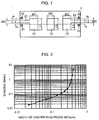
- Fig. 1 is a plan view showing this filter.
- the resonator electrodes 11, 12, and 13 have electrode lengths L1, L2, and L3, and electrode widths W1, W2, and W3, respectively.
- Each of the resonator electrodes 11, 12, and 13 functions as a microstrip line resonator which generates a half wavelength resonance at the operating frequency thereof.
- These resonators electrodes 11, 12, and 13 are arranged so that the longitudinal directions of the electrodes become parallel with one other, and so that the centers of the electrode lengths of the resonator electrodes are aligned substantially linearly from one end to the other end of the dielectric substrate, as shown by the chain line (center line) in the figure.
- Input/output electrodes 21 and 23 having width WC extend along the longitudinal direction of the filter. They are spaced apart from second ground electrodes 51 by a spacing S.
- the input/output electrodes 21 and 23 are connected to a first-stage resonator electrode 11 and a last-stage resonator electrode 13, respectively.
- the input/output electrodes 21 and 23 are connected to the first-stage resonator electrode 11 and the last-stage resonator electrode 13, respectively, at positions such that they are spaced apart from the longitudinal centers of the resonator electrodes along the longitudinal direction thereof by the spacing S. That is, the input/output electrodes 21 and 23 are formed as electrode patterns which extend from the predetermined positions of the resonance electrodes 11 and 13 to one end and the other end, respectively.
- the second ground electrodes 51 which are conductively connected to the first ground electrode on the bottom surface via through holes, are formed on both sides of each of the input/output electrodes 21 and 23, on the top surface of the dielectric substrate 1. Each of the input/output portions is thereby provided with a coplanar structure.
- the above-described resonator electrodes 11, 12, and 13, input/output electrodes 21 and 23, second ground electrodes 51, and first ground electrode on the bottom surface are formed by the thick-film printing method with respect to the surface of the dielectric substrate 1, or by the patterning of thin conductive strips.
- the through hole portions may be formed using a method similar to the conventional method wherein, after holes have been formed in the dielectric substrate 1, an electrode film is formed on the inner surface of each of the holes.
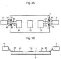
- Fig. 2 shows the relationship between the spacing S between the input/output electrodes (also referred to as the center electrodes) 21 and 23, and the second ground electrode 51, and the input/output electrode width WC when the line impedance is set to 50 ⁇ .
- the thickness of the dielectric substrate is set to 0.38 mm
- the dielectric constant is 9.6
- the frequency is 25 GHz. Even though the thickness of the dielectric substrate and the dielectric constant are constant in this way, the width WC and the spacing S can be set over a wide range, whereby the versatility in design for obtaining a predetermined line impedance is enhanced.
- the ratio (W/L) between the electrode width W and the electrode length L is set to a value smaller than 1.0 but close to 1.0, and the lead-out positions of the input/output electrodes as measured from the center in the longitudinal direction of the first-stage and last-stage resonator electrodes are shifted toward the same direction (the positions are on the same side with respect to the chain line in the figure) between the first and last resonators 11 and 13.
- the present inventor has found from his experiments that this configuration creates an attenuation pole on the higher frequency side in the pass band. The reason for this is considered to be as follows.
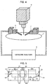
- Figs. 3A and 3B are diagrams showing a measuring method for the characteristics of the above-described filter, wherein Fig. 3A is a top view, and 3B is a side view.
- probes 6 and 7 are provided for measuring the electrical characteristics of the resonators.
- the probes 6 and 7 have center electrodes 60 and 70, and ground electrodes 61 and 62, and ground electrodes 71 and 72, respectively. By making these electrodes contact the input/output electrodes 21 and 23 of the filter and the second ground electrodes 51, the electrical conduction between these electrodes is established.
- the probes of a measuring instrument are merely abutted against the resonator electrodes and the second ground electrodes all of which are exposed two-dimensionally on the top surface of the dielectric substrate, and hence, even a small-scale filter can be measured. Furthermore, a measurement calibration can be easily performed by the probe terminal surfaces, using the so-called SOLT (Short-Open-Load-Thru) method or the like.
- SOLT Short-Open-Load-Thru
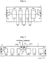
- Fig. 4 is a view illustrating how the characteristics of the above-described filters are measured and adjusted.
- a plurality of dielectric substrates 1, before being separated, are included in an aggregate substrate 1'.
- the aggregate substrate 1' is placed on an X-Y table (not shown), and the aggregate substrate is movable to arbitrary positions in the plane defined by the table, with respect to the probes 6 and 7, and a laser device 8.
- Each of the probes 6 and 7 is connected to a network analyzer 9, and is arranged so that the tip thereof contacts the input/output portions of one filter part which is at a predetermined segment of the aggregate substrate 1'.
- the contact conditions of the probes with respect to this filter part are similar to those shown in Figs. 3A and 3B.
- the laser device 8 trims predetermined portions of the resonator electrodes and dielectric substrates on the aggregate substrate.
- the trimming-off of the resonator electrode portions or the dielectric substrate portions may be performed by means of a luter or a sand-blaster, in addition to the laser trimming method.
- Fig. 5 is a plan view showing this filter.
- Second ground electrodes 51 are disposed on both sides of each of the input/output electrodes 21 and 23.
- the second ground electrodes 51 are arranged so as to be conductively connected to the first ground electrode on the bottom surface via the side electrodes on the side surfaces of the dielectric substrate 1.
- through holes are previously formed which allow the second ground electrodes 51 and the first ground electrode on the bottom surface to be conductively connected to each other, at the positions where the cutting lines (snap lines) pass when the dielectric substrate is cut off from an aggregate substrate. Then, the aggregate substrate is cut off along these cutting lines, that is, along the lines each passing through the through holes, whereby the connection portions between the second ground electrodes on the top surface and the first ground electrode on the bottom surface of the dielectric substrate are formed.
- each of the above-described resonator electrodes 11, 12, and 13 also functions as a microstrip line resonator which generates a half-wavelength resonance at the operational frequency band thereof.
- the shapes of the resonator electrodes in this second embodiment differ from those in the first embodiment.
- projections 31 and 32 are formed, respectively, on one side with respect to the center line indicated by the chain line in the figure, while in the last-stage resonator electrode 13, a projection 33 is formed on the other side with respect to the center line.
- the input/output electrodes 21 and 23 are each formed on the center line near the side surfaces of the dielectric substrate 1, but the connection positions thereof with the respective resonator electrodes 11 and 13 are formed on different sides with respect to the center line.
- An attenuation pole occurs on the lower frequency side in the pass band, when the electrode length L1, L2 and L3 of the respective resonator electrodes 11, 12, and 13 are set so that the center frequency in the pass band becomes a desired frequency, when the ratio (W/L) between the electrode width W and the electrode length L is set to be larger than 1.0 but close to 1.0, and when the lead-out positions of the input/output electrode as seen from the center in the longitudinal direction of the first-stage and last-stage resonator electrodes are shifted toward different respective directions in the first-stage resonator electrode 11 and the last-stage resonator electrodes 13.
- the electrode width W1 of the first-stage electrode 11 is not equal to the electrode width W3 of the last-stage electrode 13, and consequently the distances D1 and D2 between the three resonator electrode 11, 12, and 13 are set to different values from each other.
- projections 31, 32, and 33 are frequency adjusting electrodes which project from the resonator electrodes 11, 12, and 13, respectively, in the longitudinal direction thereof. By trimming off these portions by as much as required by the laser trimming method or the like, as shown in Fig. 4, the resonance frequency of each stage of the resonator electrodes can be adjusted.
- Fig. 6 is a top view showing a filter in accordance with a third embodiment of the present invention.
- four resonator electrodes 11 through 14 each of which constitutes a half-wavelength resonator, are disposed on a dielectric substrate 1 substantially parallel with each other, and input/output electrodes 21 and 24 are connected to the first-stage and last-stage resonator electrodes 11 and 14, respectively.
- Second (top surface) ground electrodes 51 which are conductively connected to the first ground electrode on the bottom surface, are disposed on both sides of each of the input/output electrodes 21 and 24.
- Such a structure can be obtained by forming side electrodes which connect the second ground electrodes 51 and the first ground electrode to each other, on the end faces of the dielectric substrate, after the dielectric substrate has been cut off from an aggregate substrate.
- resonator electrodes 11TX, 12TX, 13TX, 11RX, 12RX, and 13RX are formed on the top surface of a dielectric substrate 1.
- a transmitting-side circuit terminal (input/output electrode) 21TX and an antenna terminal 41 a transmission filter is formed by the three resonators by the three resonator electrodes 11TX, 12TX, and 13TX.
- a receiving-side circuit terminal (input/output electrode) 23RX and an antenna terminal 41 a reception filter is formed by the three resonators by resonator electrodes 11RX, 12RX, and 13RX.
- the input/output electrode 21TX is connected to the first-stage resonator electrode 11TX of the transmission filter, and a lead-out electrode 23TX with respect to the antenna terminal 41 is connected to the last-stage resonator electrode 13TX.
- a lead-out electrode 21RX which is connected to the antenna terminal 41, is connected to the first-stage resonator electrode 11RX of the reception filter, and the input/output electrode 23RX is connected to the last-stage resonator electrode 13RX.
- Each of the lead-out electrodes 23TX and 21RX are connected to a predetermined position of the antenna terminal 41.
- a first ground electrode is formed substantially over the entire bottom surface of the dielectric substrate 1.
- Second (top surface) ground electrodes 51 which are conductively connected to the first ground electrode on the bottom surface, are disposed on both sides of each of the input/output electrodes 23RX, 21TX, and 41.
- An electrode 41' for impedance matching extends from the connection point between the input/output electrodes 23TX and 21RX and the antenna terminal 41. Thus, impedance matching between the antenna terminal 41 and these two input/output electrodes 23TX and 21RX is achieved.
- a duplexer (an antenna sharing device) is formed wherein the input/output electrode 21TX portion as a transmitting-circuit side terminal, the input/output electrode 23RX portion as a receiving-circuit side terminal, and the antenna terminal 41 have a grounded coplanar structure.
- the transmission filter comprising the resonator electrodes 11TX, 12TX, and 13TX is fundamentally similar to the filter shown in Fig. 5, and generates an attenuation pole on the lower frequency side of the transmission frequency band which is the pass band of this filter.
- the reception filter comprising the resonator electrodes 11RX, 12RX, and 13RX is similar to the filter shown in Fig. 1, and generates an attenuation pole on the higher frequency side of the reception frequency band which is the pass band of this filter.
- this duplexer In a communication system wherein a reception frequency band is set adjacent to the lower side of a transmission frequency band, the use of this duplexer reliably prevents the mixing of transmitted signals into received signals, by the attenuation characteristics of the respective attenuation poles of the transmission filter and the reception filter.
- the second ground electrodes are provided on both sides of each of the input/output electrodes, but the second ground electrode may be disposed on only one of the sides of each of the input/output electrodes.
- each of the input/output portions is formed as a grounded coplanar structure.
- only a predetermined one of a plurality of input/output portions may be provided with a grounded coplanar structure, depending on the use of the filter or duplexer.
- reference character ANT designates a transmitting/receiving antenna, and DPX a duplexer.
- BPFa and BPFb each designates band pass filters, AMPa and AMPb amplifier circuits, and MIXa and MIXb mixers.
- OSC designates an oscillator, and SYN a synthesizer.
- MIXa mixes IF signals and signals output from SYN
- BPFa passes only the transmission frequency band among the mixed output signals from MIXa
- AMPa power-amplifies these signals and transmits them from ANT via DPX.
- AMPb amplifies the received signals output from DPX.
- BPFb passes only the reception frequency band among the output signals from AMPb.
- MIXb mixes the frequency signals output from SYN and the received signals, and outputs intermediate frequency signals IF.
- a microstrip line filter as shown in the above-described embodiments may be used, and as the DPX, a microstrip line duplexer as shown in Fig. 7 may be employed.
- each or at least some of the input/output electrode portions are formed with a grounded coplanar structure, the measurement on the electrical characteristics such as resonance frequency can be achieved by merely abutting the center electrodes of the probes of a measuring instrument against the ground electrodes, on the top surface of the dielectric substrate. Therefore, even small-scaled components can be reliably measured using a two-dimensional measuring jig.
- the electrical characteristics of the filters or duplexers are measured by abutting the probes against the input/output electrodes and the second ground electrodes, and the electrical characteristics thereof are adjusted by trimming off portions of resonator electrodes of the dielectric substrate.
Landscapes
- Physics & Mathematics (AREA)
- Electromagnetism (AREA)
- Engineering & Computer Science (AREA)
- Manufacturing & Machinery (AREA)
- Control Of Motors That Do Not Use Commutators (AREA)
Abstract
Description
Claims (13)
- A microstrip line filter, comprising:(i) a dielectric substrate (1) having a top surface and a bottom surface;(ii) a plurality of resonator electrodes (11,12,13,14) which is provided on the top surface of said dielectric substrate (1), and which includes at least a first-stage resonator electrode (11) and a last-stage resonator electrode (13;14);(iii) an input/output electrode (21,23;24) which is connected to at least one of said first-stage (11) and last-stage resonator electrodes (13,14), and which is provided on the top surface of said dielectric substrate (1);(iv) a first ground electrode (5) which is provided on the bottom surface of said dielectric substrate (1), and which is disposed so as to be opposed to said resonator electrodes (11,12,13,14) with said dielectric substrate (1) therebetween; and(v) at least one second ground electrode (51) which is provided on the top surface of said dielectric substrate (1), and which is conductively connected to said first ground electrode (5).
- A microstrip line filter in accordance with claim 1, wherein said second ground electrode (5) is provided adjacent to said input/output electrode (21,23,24).
- A microstrip line filter in accordance with claim 1 or 2, wherein said at least one second ground electrode (51) includes second ground electrodes which are provided respectively on both sides of said input/output electrode (21,23,24).
- A microstrip line filter in accordance with one of claims 1 to 3, wherein said first ground electrode (5) and said second ground electrode (51) are connected via a through hole provided in said dielectric substrate (1).
- A microstrip line filter in accordance with one of claims 1 to 3, wherein said first ground electrode (5) and said second ground electrode (51) are connected via a side electrode provided on the side surface of said dielectric substrate (1).
- A microstrip line filter in accordance with one of claims 1 to 5, wherein said plurality of resonator electrodes (11,12,13;14) is arranged in line from a first end of said dielectric substrate to an opposite second end thereof.
- A microstrip line filter in accordance with one of claims 1 to 6, wherein the input/output electrode (21) connected to said first-stage resonator electrode (11) is provided at one end of said dielectric substrate (1), while the input/output electrode (23;24) connected to said last-stage resonator electrode (13;14) is provided at the other end of said dielectric substrate (1).
- A duplexer comprising:a transmitting-circuit side terminal (21TX), a receiving-circuit side terminal (23RX), and an antenna terminal (41);microstrip line filter in accordance with claim 1, said microstrip line filter being provided between said transmitting-circuit side terminal (21TX) and said antenna terminal (41), and/or between said receiving-circuit side terminal (23RX) and said antenna terminal (41).
- A communication device comprising:
a high-frequency communication circuit, and connected thereto, a microstrip line filter in accordance with one of claims 1 to 7. - A communication device comprising:
a high-frequency communication circuit, and connected thereto, a duplexer in accordance with one of claims 1 to 7. - A method for adjusting the electrical characteristics of a microstrip line type resonator, said method comprising the steps of:(a) providing an aggregate substrate (1) which includes a plurality of microstrip line type resonators, each of said microstrip line type resonators comprising:(i) a dielectric (I) having a top surface and a bottom surface;(ii) a plurality of resonator electrodes (11,12,13;14) which is provided on the top surface of said dielectric substrate (1), and which includes at least a first-stage resonator electrode (11) and a last-stage resonator electrode (13;14);(iii) an input/output electrode (21,23;24) which is connected to at least one of said first-stage and last-stage resonator electrodes (11,13;14), and which is provided on the top surface of said dielectric substrate (1);(iv) a first ground electrode (5) which is provided on the bottom surface of said dielectric substrate (1), and which is disposed so as to be opposed to said resonator electrodes (11,12,13;14) with said dielectric substrate (1) therebetween; and(v) at least one second ground electrode (51) which is provided on the top surface of said dielectric substrate (1), and which is conductively connected to said first ground electrode (5),(b) placing (6,7) probes of a measuring instrument (9) for measuring the electrical characteristics of said microstrip line type resonators in contact with said input/output electrodes (21,23;24) and said second ground electrodes (51), on said aggregate substrate (1), and(c) adjusting the electric characteristics of said microstrip line type resonators while measuring the electrical characteristics of said microstrip line type resonators.
- A method for adjusting the electrical characteristics of a microstrip line type resonator in accordance with claim 11, wherein the resonance frequency of said microstrip line type resonator is adjusted by trimming said resonator electrodes (11,12,13;14).
- A method for adjusting the electrical characteristics of a microstrip line type resonator in accordance with claim 11 or 12, wherein the resonance frequency of said microstrip line type resonator is adjusted by trimming said dielectric substrate (1).
Applications Claiming Priority (2)
| Application Number | Priority Date | Filing Date | Title |
|---|---|---|---|
| JP2000138253 | 2000-05-11 | ||
| JP2000138253 | 2000-05-11 |
Publications (2)
| Publication Number | Publication Date |
|---|---|
| EP1154511A2 true EP1154511A2 (en) | 2001-11-14 |
| EP1154511A3 EP1154511A3 (en) | 2003-05-07 |
Family
ID=18645893
Family Applications (1)
| Application Number | Title | Priority Date | Filing Date |
|---|---|---|---|
| EP01110330A Withdrawn EP1154511A3 (en) | 2000-05-11 | 2001-04-26 | Adjusting method for electrical characteristics of microstrip line filter, duplexer, communication device, and microstrip line type resonator |
Country Status (3)
| Country | Link |
|---|---|
| US (1) | US6603373B2 (en) |
| EP (1) | EP1154511A3 (en) |
| KR (1) | KR100397730B1 (en) |
Cited By (1)
| Publication number | Priority date | Publication date | Assignee | Title |
|---|---|---|---|---|
| CN109066039A (en) * | 2018-06-25 | 2018-12-21 | 南京师范大学 | A kind of novel micro-strip function divides duplexer |
Families Citing this family (6)
| Publication number | Priority date | Publication date | Assignee | Title |
|---|---|---|---|---|
| JP2003309406A (en) * | 2002-04-16 | 2003-10-31 | Murata Mfg Co Ltd | Resonator, filter, composite filter device, transceiver, and communication apparatus |
| AU2003203729B2 (en) * | 2002-04-17 | 2005-10-13 | Lg Electronics Inc. | Pulsator and washing machine using the same |
| TWI256747B (en) * | 2005-06-01 | 2006-06-11 | Accton Technology Corp | Antenna structure |
| JP4327802B2 (en) * | 2006-01-23 | 2009-09-09 | 株式会社東芝 | Filter and wireless communication apparatus using the same |
| KR200456383Y1 (en) | 2009-03-05 | 2011-10-27 | 주식회사 티큐브텍 | Frequency Combiner and Combining Apparatus |
| KR102176634B1 (en) * | 2019-01-02 | 2020-11-10 | 중앙대학교 산학협력단 | Device and method for resonant characteristic prediction using intensities of discrete wavelength points |
Family Cites Families (14)
| Publication number | Priority date | Publication date | Assignee | Title |
|---|---|---|---|---|
| US4168479A (en) * | 1977-10-25 | 1979-09-18 | The United States Of America As Represented By The Secretary Of The Navy | Millimeter wave MIC diplexer |
| JPS5873203A (en) * | 1981-10-28 | 1983-05-02 | Hitachi Ltd | Manufacturing method of thick film filter |
| US4551696A (en) * | 1983-12-16 | 1985-11-05 | Motorola, Inc. | Narrow bandwidth microstrip filter |
| JP2668423B2 (en) | 1988-11-24 | 1997-10-27 | 富士通株式会社 | High frequency circuit measuring device |
| US5172084A (en) * | 1991-12-18 | 1992-12-15 | Space Systems/Loral, Inc. | Miniature planar filters based on dual mode resonators of circular symmetry |
| US5703544A (en) * | 1996-03-13 | 1997-12-30 | Ericsson Inc. | RF printed circuit module and method of making same |
| JPH10145110A (en) * | 1996-11-05 | 1998-05-29 | Murata Mfg Co Ltd | Composite dielectric filter |
| JPH10294604A (en) * | 1997-04-18 | 1998-11-04 | Seiko Epson Corp | High frequency circuit and method of manufacturing the same |
| US6181225B1 (en) * | 1998-02-17 | 2001-01-30 | Itron, Inc. | Laser tunable thick film microwave resonator for printed circuit boards |
| JP3633280B2 (en) * | 1998-05-29 | 2005-03-30 | 松下電器産業株式会社 | Half-wave resonator type high frequency filter |
| JP3331967B2 (en) * | 1998-06-02 | 2002-10-07 | 松下電器産業株式会社 | Millimeter wave module |
| JP2000068701A (en) * | 1998-08-24 | 2000-03-03 | Matsushita Electric Ind Co Ltd | Millimeter wave module |
| US6313719B1 (en) * | 2000-03-09 | 2001-11-06 | Avaya Technology Corp. | Method of tuning a planar filter with additional coupling created by bent resonator elements |
| JP3848051B2 (en) * | 2000-04-28 | 2006-11-22 | 株式会社デンソー | Resonant frequency measuring method and resonant frequency measuring apparatus |
-
2001
- 2001-04-26 EP EP01110330A patent/EP1154511A3/en not_active Withdrawn
- 2001-05-11 US US09/854,263 patent/US6603373B2/en not_active Expired - Fee Related
- 2001-05-11 KR KR10-2001-0025738A patent/KR100397730B1/en not_active Expired - Fee Related
Cited By (1)
| Publication number | Priority date | Publication date | Assignee | Title |
|---|---|---|---|---|
| CN109066039A (en) * | 2018-06-25 | 2018-12-21 | 南京师范大学 | A kind of novel micro-strip function divides duplexer |
Also Published As
| Publication number | Publication date |
|---|---|
| US20020003460A1 (en) | 2002-01-10 |
| US6603373B2 (en) | 2003-08-05 |
| KR20010104269A (en) | 2001-11-24 |
| EP1154511A3 (en) | 2003-05-07 |
| KR100397730B1 (en) | 2003-09-13 |
Similar Documents
| Publication | Publication Date | Title |
|---|---|---|
| KR100319474B1 (en) | dielectric filter, dielectric duplexer and communication apparatus | |
| EP1439599B1 (en) | Waveguide-Type dielectric filter | |
| US6603373B2 (en) | Adjusting method for electrical characteristics of microstrip line filter, duplexer, communication device, and microstrip line type resonator | |
| US6538526B2 (en) | Transmission line connection structure, high frequency module, and communication device | |
| GB2374985A (en) | Dielectric filter, dielectric duplexer, and communication apparatus | |
| KR100367860B1 (en) | Method for forming input-output electrode of the dielectric resonant device | |
| US7253698B2 (en) | Line converter for coupling standing waves to a shield area of a three dimensional waveguide | |
| KR100411203B1 (en) | Dielectric Filter, Dielectric Duplexer and Communication Apparatus incorporating the Same | |
| KR100352573B1 (en) | Dielectric Filter, Dielectric Duplexer, and Communication Apparatus | |
| KR100394804B1 (en) | Dielectric filter, dielectric duplexer, communication system, and method of producing dielectric filter | |
| US6232854B1 (en) | Dielectric resonator device, dielectric filter, oscillator, sharing device, and electronic apparatus | |
| KR100405325B1 (en) | Dielectric filter, dielectric duplexer, and communication apparatus incorporating the same | |
| JP2002033604A (en) | Microstrip line filter, duplexer, communication unit and method for adjusting characteristic of resonator | |
| US6580339B2 (en) | Dielectric duplexer and communication apparatus | |
| US6784767B2 (en) | Dielectric filter, dielectric duplexer, and communication apparatus | |
| US6476687B1 (en) | Dielectric filter providing TEM- and TE-mode resonators and communicaton device using the same | |
| CN120674777A (en) | Waveguide converter | |
| JP2000022405A (en) | Composite filter, antenna multicoupler and communication equipment | |
| JP2001298308A (en) | Dielectric resonator, communication equipment and production method for dielectric resonator |
Legal Events
| Date | Code | Title | Description |
|---|---|---|---|
| PUAI | Public reference made under article 153(3) epc to a published international application that has entered the european phase |
Free format text: ORIGINAL CODE: 0009012 |
|
| 17P | Request for examination filed |
Effective date: 20010426 |
|
| AK | Designated contracting states |
Kind code of ref document: A2 Designated state(s): AT BE CH CY DE DK ES FI FR GB GR IE IT LI LU MC NL PT SE TR |
|
| AX | Request for extension of the european patent |
Free format text: AL;LT;LV;MK;RO;SI |
|
| PUAL | Search report despatched |
Free format text: ORIGINAL CODE: 0009013 |
|
| AK | Designated contracting states |
Designated state(s): AT BE CH CY DE DK ES FI FR GB GR IE IT LI LU MC NL PT SE TR |
|
| AX | Request for extension of the european patent |
Extension state: AL LT LV MK RO SI |
|
| AKX | Designation fees paid |
Designated state(s): DE FR GB |
|
| 17Q | First examination report despatched |
Effective date: 20070803 |
|
| RAP1 | Party data changed (applicant data changed or rights of an application transferred) |
Owner name: MURATA MANUFACTURING CO., LTD. |
|
| STAA | Information on the status of an ep patent application or granted ep patent |
Free format text: STATUS: THE APPLICATION IS DEEMED TO BE WITHDRAWN |
|
| 18D | Application deemed to be withdrawn |
Effective date: 20071214 |