EP1152475A1 - Thin-film piezoelectric device - Google Patents
Thin-film piezoelectric device Download PDFInfo
- Publication number
- EP1152475A1 EP1152475A1 EP00921111A EP00921111A EP1152475A1 EP 1152475 A1 EP1152475 A1 EP 1152475A1 EP 00921111 A EP00921111 A EP 00921111A EP 00921111 A EP00921111 A EP 00921111A EP 1152475 A1 EP1152475 A1 EP 1152475A1
- Authority
- EP
- European Patent Office
- Prior art keywords
- thickness
- film
- acoustic wave
- wave device
- normalized
- Prior art date
- Legal status (The legal status is an assumption and is not a legal conclusion. Google has not performed a legal analysis and makes no representation as to the accuracy of the status listed.)
- Withdrawn
Links
Images











Classifications
-
- H—ELECTRICITY
- H10—SEMICONDUCTOR DEVICES; ELECTRIC SOLID-STATE DEVICES NOT OTHERWISE PROVIDED FOR
- H10N—ELECTRIC SOLID-STATE DEVICES NOT OTHERWISE PROVIDED FOR
- H10N30/00—Piezoelectric or electrostrictive devices
-
- H—ELECTRICITY
- H03—ELECTRONIC CIRCUITRY
- H03H—IMPEDANCE NETWORKS, e.g. RESONANT CIRCUITS; RESONATORS
- H03H9/00—Networks comprising electromechanical or electro-acoustic elements; Electromechanical resonators
- H03H9/15—Constructional features of resonators consisting of piezoelectric or electrostrictive material
- H03H9/17—Constructional features of resonators consisting of piezoelectric or electrostrictive material having a single resonator
- H03H9/171—Constructional features of resonators consisting of piezoelectric or electrostrictive material having a single resonator implemented with thin-film techniques, i.e. of the film bulk acoustic resonator [FBAR] type
- H03H9/172—Means for mounting on a substrate, i.e. means constituting the material interface confining the waves to a volume
- H03H9/174—Membranes
-
- H—ELECTRICITY
- H03—ELECTRONIC CIRCUITRY
- H03H—IMPEDANCE NETWORKS, e.g. RESONANT CIRCUITS; RESONATORS
- H03H3/00—Apparatus or processes specially adapted for the manufacture of impedance networks, resonating circuits, resonators
- H03H3/007—Apparatus or processes specially adapted for the manufacture of impedance networks, resonating circuits, resonators for the manufacture of electromechanical resonators or networks
- H03H3/02—Apparatus or processes specially adapted for the manufacture of impedance networks, resonating circuits, resonators for the manufacture of electromechanical resonators or networks for the manufacture of piezoelectric or electrostrictive resonators or networks
- H03H3/04—Apparatus or processes specially adapted for the manufacture of impedance networks, resonating circuits, resonators for the manufacture of electromechanical resonators or networks for the manufacture of piezoelectric or electrostrictive resonators or networks for obtaining desired frequency or temperature coefficient
-
- H—ELECTRICITY
- H03—ELECTRONIC CIRCUITRY
- H03H—IMPEDANCE NETWORKS, e.g. RESONANT CIRCUITS; RESONATORS
- H03H9/00—Networks comprising electromechanical or electro-acoustic elements; Electromechanical resonators
- H03H9/02—Details
- H03H9/02007—Details of bulk acoustic wave devices
- H03H9/02086—Means for compensation or elimination of undesirable effects
- H03H9/02133—Means for compensation or elimination of undesirable effects of stress
-
- H—ELECTRICITY
- H03—ELECTRONIC CIRCUITRY
- H03H—IMPEDANCE NETWORKS, e.g. RESONANT CIRCUITS; RESONATORS
- H03H9/00—Networks comprising electromechanical or electro-acoustic elements; Electromechanical resonators
- H03H9/02—Details
- H03H9/02007—Details of bulk acoustic wave devices
- H03H9/02157—Dimensional parameters, e.g. ratio between two dimension parameters, length, width or thickness
-
- H—ELECTRICITY
- H03—ELECTRONIC CIRCUITRY
- H03H—IMPEDANCE NETWORKS, e.g. RESONANT CIRCUITS; RESONATORS
- H03H9/00—Networks comprising electromechanical or electro-acoustic elements; Electromechanical resonators
- H03H9/15—Constructional features of resonators consisting of piezoelectric or electrostrictive material
-
- H—ELECTRICITY
- H03—ELECTRONIC CIRCUITRY
- H03H—IMPEDANCE NETWORKS, e.g. RESONANT CIRCUITS; RESONATORS
- H03H9/00—Networks comprising electromechanical or electro-acoustic elements; Electromechanical resonators
- H03H9/15—Constructional features of resonators consisting of piezoelectric or electrostrictive material
- H03H9/17—Constructional features of resonators consisting of piezoelectric or electrostrictive material having a single resonator
- H03H9/176—Constructional features of resonators consisting of piezoelectric or electrostrictive material having a single resonator consisting of ceramic material
-
- H—ELECTRICITY
- H03—ELECTRONIC CIRCUITRY
- H03H—IMPEDANCE NETWORKS, e.g. RESONANT CIRCUITS; RESONATORS
- H03H3/00—Apparatus or processes specially adapted for the manufacture of impedance networks, resonating circuits, resonators
- H03H3/007—Apparatus or processes specially adapted for the manufacture of impedance networks, resonating circuits, resonators for the manufacture of electromechanical resonators or networks
- H03H3/02—Apparatus or processes specially adapted for the manufacture of impedance networks, resonating circuits, resonators for the manufacture of electromechanical resonators or networks for the manufacture of piezoelectric or electrostrictive resonators or networks
- H03H3/04—Apparatus or processes specially adapted for the manufacture of impedance networks, resonating circuits, resonators for the manufacture of electromechanical resonators or networks for the manufacture of piezoelectric or electrostrictive resonators or networks for obtaining desired frequency or temperature coefficient
- H03H2003/0414—Resonance frequency
- H03H2003/0421—Modification of the thickness of an element
- H03H2003/0428—Modification of the thickness of an element of an electrode
Definitions
- the present invention relates to a film bulk acoustic device using an acoustic wave such as resonators and filters.
- Figs. 1 and 2 show this type of the conventional film bulk acoustic wave device as described in, for example, the literature “Bulk-Acoustic-Wave Devices using the Second-Order Thickness-Extensional Mode in Thin ZnO-SiO 2 Composite Films on Si", Proceedings of The Acoustical Society of Japan, pp. 691-692, Sept.-Oct. 1985 (hereinafter, referred to as reference 1), and the literature “Fundamental Bulk Acoustic Resonators in GHz Range", Proceedings of The Institutes of Electronics, Information and Communication Engineers, vol.81, No.5, pp.468-472, 1998 (hereinafter, referred to as reference 2).
- Fig. 1 is a top view
- Fig. 1 is a top view
- reference numeral 1 denotes a silicon (Si) substrate; 2 denotes a silicon oxide (SiO 2 ) formed on the silicon substrate 1; 3 denotes a bottom electrode formed on the silicon oxide 2; 4 denotes a piezoelectric film composed of zinc oxide (ZnO) formed on the bottom electrode 3; 5 denotes a top electrode, divided into input-side electrode 5a and output-side electrode 5b, formed on the piezoelectric film 4; and 6 denotes a via hole.
- Si silicon
- SiO 2 silicon oxide
- 3 denotes a bottom electrode formed on the silicon oxide 2
- 4 denotes a piezoelectric film composed of zinc oxide (ZnO) formed on the bottom electrode 3
- 5 denotes a top electrode, divided into input-side electrode 5a and output-side electrode 5b, formed on the piezoelectric film 4
- 6 denotes a via hole.
- the acoustic wave in the piezoelectric film 4 at this moment comes to be a cut-off mode at a frequency lower than a certain frequency f 0 , and comes to be a propagation mode at a frequency higher than the frequency f 0 .
- the frequency f 0 is a cut-off frequency, and corresponds to a frequency in which the thickness 2h of the piezoelectric film 4 coincides with a half wavelength of the acoustic wave propagating in the thickness direction in the piezoelectric film 4 when the two surfaces of the piezoelectric film 4 are free surfaces.
- the cut-off frequency f m0 of the electrode unit is lower than the cut-off frequency f f0 of a non-electrode unit provided with only the bottom electrode 3, due to the electrode thickness and mass load.
- the acoustic wave is the propagation mode due to a higher frequency side than the cut-off frequency f m0 in the electrode unit, while it is the cut-off mode due to a lower frequency side than the cut-off frequency f f0 in the non-electrode unit.
- the acoustic wave propagating in parallel to the surface of the film 4 results in a state that an energy is trapped in the top electrode 5.
- the characteristics of such a filter are determined by the thickness 2h of the piezoelectric film 4, the thickness of the top electrode 5, the thickness g of the silicon oxide 2, the shape of the top electrode 5, and a gap between the input-side electrode 5a and the output-side electrode 5b.
- the reference 1 describes one example in which a normalized thickness (g/h) of the piezoelectric film 4 is 1.54 and 2.4, which is determined by the thickness 2h of the piezoelectric film 4 and the thickness g of the silicon oxide 2.
- the reference 1 also represents that the design is made by focusing the temperature characteristics and the loss of the acoustic wave.
- the reference 1 designates to use an acoustic wave of the second mode.
- the acoustic wave is a fundamental mode (first mode) when a gap between the surface of the top electrode 5 and the back of the silicon oxide 2 is a half wave length of the acoustic wave, and an N-th mode (N: integer) corresponds to an N multiple of the wave length of the fundamental mode.
- Fig. 3 shows this type of the conventional film bulk acoustic device described in, for example, JP-A 6-350154 (hereinafter, referred to as reference 3).
- Fig. 3 is a cross sectional view.
- a piezoelectric film 7 is composed of lead titanate-zirconate (PZT);
- a bottom electrode 3 is composed of a titanium (Ti) film 8 and a platinum (Pt) film 9;
- a top electrode 5 is composed of a titanium film 10 and a gold (Au) film 11.
- the reference 3 describes one example in which a normalized thickness (d/h) of the bottom electrode 3 is 1.0, which is determined by the thickness 2h of the piezoelectric film 7 and the thickness d of the bottom electrode 3.
- the reference 3 designates that favorable piezoelectric characteristics may be performed by an appropriate composition ratio of lead titanate (PbTiO 3 ) and lead zirconate (PbZrO 3 ).
- the piezoelectric film 7 composed of lead titanate-zirconate excites a thickness extension vibration as a main vibration.
- the acoustic wave propagating in parallel with the surface of the piezoelectric film 7 designates the dispersion characteristics as shown in Fig. 4.
- the horizontal axis corresponds to a normalized thickness of the piezoelectric film 7 which multiplies the wave number k of the acoustic wave propagating in parallel with the surface of the film 7, and the thickness of the piezoelectric film 7 together, that is, a normalized piezoelectric thickness (2kh), while the vertical axis corresponds to a frequency.
- a range that the normalized piezoelectric substance thickness is a real number is a range that the acoustic wave is a propagation mode, while a range that the normalized piezoelectric substance thickness is an imaginary number is a range that the acoustic wave is a cut-off mode.
- the frequency at the crossing point with the vertical axis, such that the normalized thickness is zero is a cut-off frequency f 0 .
- the first mode (TE1) of the thickness extension vibration shows a characteristic that the frequency is made lower as the normalized piezoelectric substance thickness is larger in the vicinity of the vertical axis.
- this is also applied similarly in a piezoelectric film having the thickness extension vibration as a main vibration, constituting lead titanate (PbTiO 3 ), lithium tantalate (LiTaO 3 ), or a material having the Poisson's ratio of one-third or less.
- the cut-off mode corresponds to a frequency higher than the cut-off frequency f m0 in a range that the top electrode 5 exists, while the propagation mode corresponds to a frequency lower than the cut-off frequency f f0 in a range that the top electrode 5 is absent. Therefor, a favorable energy trapping cannot be performed, resulting in enlarged loss.
- the variations of the characteristics of the filter may be enlarged under the influence of the ambience of the top electrode 5.
- JP-B 58/58828 (hereinafter, referred to as reference 4) has been used. That is, an addition is added to lead titanate-zirconate, so that the Poisson's ratio of the lead titanate-zirconate mixed with the addition can be one-third or more.
- the characteristics like the first mode (TE1) of the thickness extension vibration in Fig. 4 it is set to show up the following characteristics: the frequency is higher as the thickness of the normalized piezoelectric substance is larger in the vicinity of the vertical axis, thereby performing the same energy trapping as a case where the piezoelectric film 4 composed of lead oxide are applied. Note that when the Poisson's ratio exceeds one-third, the cut-off frequency of the first mode (TE1) of the thickness extension vibration is higher than that of the second mode (TS2) of the thickness shear vibration.
- This type of the conventional film bulk acoustic wave device which enables to perform the energy trapping is limited by a piezoelectric film composed of a material such as zinc oxide which generates the thickness shear vibration as a main vibration. For this reason, there is a drawback such that it is difficult to flexibly correspond to a variety of characteristics necessary for a filter.
- the energy-trapping has been performed by bringing the Poisson's ratio to one-third or more with mixing an addition to the material.
- the method described in the reference 4 can be performed only by a fabrication method which sinters piezoelectric ceramics. When the method is applied to a piezoelectric film, it is difficult to maintain favorably the quality of the piezoelectric film, resulting in deteriorating the characteristics of film bulk acoustic wave devices.
- the present invention has been made to solve the aforementioned drawbacks, and an object of this invention is to obtain a film bulk acoustic wave device which enables an energy trapping with a piezoelectric film for exciting or generating a thickness extension vibration as a main vibration, thereby providing a more favorable characteristic than the prior art.
- a film bulk acoustic wave device comprises: a substrate; a dielectric film including a silicon nitride (SiN) formed on the substrate and a silicon oxide (SiO 2 ) on the silicon nitride; a bottom electrode formed on the dielectric film; a piezoelectric film formed on the bottom electrode; and a top electrode formed on the piezoelectric film, wherein a via hole is formed in such a manner that the thickness direction of a part of the substrate which is opposite to a region including a part where the top electrode exists is removed from the bottom surface of the substrate to a boundary surface with the silicon nitride.
- SiN silicon nitride
- SiO 2 silicon oxide
- the breakdown of the components upon the etching to form a via hole may be prevented through the silicon nitride, and simultaneously, the inferiority of the characteristics of the components due to the deformation caused by the inner stress upon forming the via hole may be prevented.
- the silicon oxide is formed separately on the silicon nitride and on the top electrode.
- the errors on fabrication may be adjusted by the silicon oxide formed on the top electrode, and simultaneously, the top electrode may be protected.
- the piezoelectric film In the film bulk acoustic wave device according to this invention, the piezoelectric film generates a thickness extension vibration as a main vibration, and in order to prevent the thickness of the silicon nitride from affecting the vibration characteristics, the thickness of the silicon oxide is larger than that of the silicon nitride, and 1.5 times or more the thickness of the piezoelectric film.
- an energy trapping possible film bulk acoustic wave device may be performed, which has an effective electromechanical coupling coefficient k 2 larger than this type of the conventional film bulk acoustic wave device and has the characteristics of wider range and reduced loss, thereby preventing unnecessary spurious occurrences caused by the end shape of the piezoelectric substance originally irrelevant to the characteristics of the film bulk acoustic wave device, a positional relationship between the end of the piezoelectric substance and the end of the via hole, and so on, and further preventing enlarged loss when the energy of an acoustic wave propagates to the outside of the top electrode.
- the film bulk acoustic wave device may perform an energy trapping by use of the second mode (TE2) of the thickness extension vibration, and further has a larger electromechanical coupling coefficient than this type of the conventional film bulk acoustic wave device and little occurs a thickness shear vibration other than the thickness extension vibration as a main vibration, thereby achieving the characteristics of a wider range and a lower loss than the prior art.
- TE2 the second mode
- the film bulk acoustic wave device may perform an energy trapping by use of the second mode (TE2) of the thickness extension vibration, and further has a larger electromechanical coupling coefficient than this type of the conventional film bulk acoustic wave device and little occurs a thickness shear vibration other than the thickness extension vibration as a main vibration, thereby achieving the characteristics of a wider range and a lower loss than the prior art.
- TE2 the second mode
- the dielectric film has a silicon nitride (SiN) formed on the substrate, and a via hole is formed in such a manner that the thickness direction of a part of the substrate which is opposite to a region including a part where the top electrode exists is removed from the bottom surface of the substrate to a boundary surface with the silicon nitride.
- SiN silicon nitride
- the breakdown of the components upon the etching to form a via hole may be prevented through the silicon nitride, and simultaneously, the inferiority of the characteristics of the components due to the deformation caused by the inner stress upon forming the via hole may be prevented.
- the silicon oxide is formed separately on the substrate and on the top electrode.
- the error of the thickness upon fabrication may be adjusted and simultaneously, the top electrode may be protected.
- the bottom electrode is mainly composed of either platinum (Pt) or iridium (Ir).
- the piezoelectric film has as a main component either one of lead titanate (PbTiO 3 ), lead titanate-zirconate (PZT), lithium tantalate (LiTaO 3 ), and a material having the Poisson's ratio less than 0.33.
- a flexible countermeasure may be performed in accordance with the characteristics required for the film bulk acoustic wave device.
- Fig. 1 is a top view showing a conventional film bulk acoustic wave device having a piezoelectric film composed of zinc oxide.
- Fig. 2 is a cross sectional view showing the conventional film bulk acoustic wave device having a piezoelectric film composed of zinc oxide.
- Fig. 3 is a cross sectional view showing a conventional film bulk acoustic wave device having a piezoelectric film composed of PZT.
- Fig. 4 is a graph showing dispersion characteristics of the conventional film bulk acoustic wave device having a piezoelectric film composed of PZT.
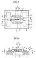
- Fig. 5 is a top view showing a film bulk acoustic wave device according to Embodiment 1 of the present invention.
- Fig. 6 is a cross sectional view showing the film bulk acoustic wave device according to Embodiment 1 of this invention.
- Fig. 11 is a graph showing a relationship between the normalized thickness of the top electrode and the normalized SiO 2 thickness when the electromechanical coupling coefficient k 2 satisfies a certain condition.
- Fig. 21 is a graph showing the electromechanical coupling coefficient characteristics of the film bulk acoustic wave device according to Embodiment 2 of this invention.
- Fig. 26 is a graph showing the normalized SiO 2 thickness in which the TE2 mode crosses the TS3 mode of the film bulk acoustic wave device according to Embodiment 2 of this invention when the horizontal axis is designated as the normalized electrode thickness.
- Fig. 27 is a graph showing the normalized SiO 2 thickness in which the TE2 mode crosses the TS3 mode of the film bulk acoustic wave device according to Embodiment 2 of this invention when the horizontal axis is designated as the equivalent density.
- Fig. 31 is a graph showing the normalized SiO 2 thickness in which the TE2 mode crosses the TS3 mode of the film bulk acoustic wave device according to Embodiment 3 of this invention when the horizontal axis is designated as the normalized electrode thickness.
- Fig. 32 is a graph showing the normalized SiO 2 thickness in which the TE2 mode crosses the TS3 mode of the film bulk acoustic wave device according to Embodiment 3 of this invention when the horizontal axis is designated as the equivalent density.
- Fig. 33 is a graph showing the normalized cut-off frequency characteristics of the film bulk acoustic wave device according to Embodiment 3 of this invention when the acoustic constant is varied.
- Fig. 34 is a graph showing the normalized cut-off frequency characteristics of the film bulk acoustic wave device according to Embodiment 3 of this invention when the density is varied.
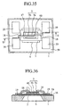
- Fig. 35 is a top view showing a film bulk acoustic wave device according to Embodiment 7 of this invention.
- Fig. 36 is a cross sectional view showing the film bulk acoustic wave device according to Embodiment 7 of this invention.
- Fig. 37 is a cross sectional view showing a modification of the film bulk acoustic wave device.
- Figs. 5 and 6 show a film bulk acoustic wave device 4 according to an embodiment 1 of the present invention.
- Fig. 5 is a top view; and
- Fig. 6 is a cross sectional view taken along line II-II.
- reference numeral 1 denotes a silicon (Si) substrate;
- 21 denotes a dielectric film formed on the silicon substrate 1, and composed of a silicon nitride (SiN) 16 formed on the silicon substrate 1 and a silicon oxide (SiO 2 ) 2 formed thereon, in this embodiment.
- 3 denotes a bottom electrode formed on the dielectric film 21, and composed of a titanium (Ti) film formed on the silicon oxide 2 and a platinum (Pt) film formed thereon, in this embodiment.
- a via hole 6 is formed by removing the bottom surface of the silicon substrate 1 to the boundary surface of the silicon nitride 16 in the thickness direction of a part of the silicon substrate 1 opposite to a region including a part provided with the top electrode 5.
- the silicon nitride 16 is particularly favorable in the resistance to an etching solution so as to form the via hole 6 and in the characteristics to an inner stress for achievement of a flat surface, and is particularly suitable for formation of the surface in contact with the via hole 6. Hence, the application of the silicon nitride 16 may prevent the breakdown of elements during etching and also prevent the deterioration of the characteristics of the elements due to the deformation caused by the inner stress.
- the titanium film of the bottom electrode 3 is inserted for improvement of an adhesion between the platinum film formed thereon and the dielectric film 21.
- the crystallinity of the platinum film of the bottom electrode 3 is very important so as to obtain a favorable piezoelectric film 17 since the piezoelectric film 17 grows along the crystal lattice of the platinum film.
- the platinum film of the top electrode 5 is used because of its relatively excellent characteristics with respect to corrosion-resistance and electrical resistance.
- the thickness of the platinum film is relatively thicker than that of the titanium film. For example, it is designated by a relationship of the platinum film: 0.1 ⁇ m thick and the titanium film: 0.03 ⁇ m thick.
- the thickness of the piezoelectric film 17 is set to 2h; the thickness of the top electrode 5 is set to d1; the thickness of the bottom electrode 3 is set to d2; and the thickness of the dielectric film 21 is set to g.
- the platinum film is thicker than the titanium film, and further the density of platinum is 21370 kg/m 3 , while the density of titanium is 4540 kg/m 3 .
- the thickness of the platinum film is used as a central value when the thickness of the top electrode 5 is d1 and the thickness of the bottom electrode 3 is d2.
- the silicon nitride 16 and the silicon oxide 2 since there is no critical difference between the silicon nitride 16 and the silicon oxide 2, the sum in thickness of the silicon nitride 16 and the silicon oxide 2 is used when the thickness of the dielectric film 21 is g.
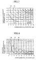
- Figs. 7 and 8 are graphs showing the characteristics of the film bulk acoustic wave device according to Embodiment 1. These show the characteristics when the top electrode 5 and bottom electrode 3 are composed of platinum, the piezoelectric film 17 is composed of lead titanate, and the dielectric film 21 is composed of silicon oxide. Figs. 7 and 8 show the calculation results in a case where both the normalized thickness d1/h of the top electrode 5 determined by the thickness 2h of the piezoelectric film 17 and the thickness d1 of the top electrode 5, and the normalized thickness d2/h of the bottom electrode 3 determined by the thickness 2h of the piezoelectric film 17 and the thickness d2 of the bottom electrode 3 is 0.02.
- the horizontal axes in Figs. 7 and 8 are the normalized thickness of the dielectric film 21, that is, normalized SiO 2 thickness (g/h), determined by the thickness 2h of the piezoelectric film 17 and the thickness g of the piezoelectric film 21, that is, normalized SiO 2 thickness (g/h).
- the vertical axis in Fig. 7 is the normalized resonant frequency Fr/f 0 when the resonant frequency Fr of the electrode unit is normalized by the resonant frequency f 0 in thickness resonance when both surfaces of the electrode unit are free surfaces.
- An equivalent circuit by use of distribution constant lines is used in the calculations.
- This equivalent circuit is the same as that of an equivalent circuit, for example, as shown of Fig. 3 in JP-A 9-130200 (hereinafter, referred to as reference 5).
- the impedance estimated from the electrical terminals of the equivalent circuit is calculated with varying frequencies; a frequency in which the impedance is closest to zero is set to the resonant frequency Fr, while a frequency in which an admittance as a reverse number of the impedance is closest to zero is set to the antiresonant frequency Fa.
- reference numeral 21 and 24 each denote the characteristics of a first mode (TE1) of the thickness extension vibration; 22 and 25 each denote the characteristics of a second mode (TE2) of the thickness extension vibration; and 23 and 26 each denote the characteristics of a third mode (TE3) thereof.
- the normalized resonant frequency of the first mode (TE1) is a slightly smaller value than 0.4 when the normalized SiO 2 thickness is zero; the thicker the normalized SiO 2 thickness, the smaller the resonant frequency Fr. Similarly, the thicker the normalized SiO 2 thickness, the smaller the resonant frequencies of the second mode (TE2) and third mode (TE3).
- the electromechanical coupling coefficient k 2 of the first mode (TE1) is substantially maximum when the normalized SiO 2 thickness is approximate to zero, while the larger the normalized SiO 2 thickness, the smaller the coefficient k 2 .
- the electromechanical coupling coefficient k 2 of the second mode (TE2) is maximum around the normalized SiO 2 thickness of 3, while the electromechanical coupling coefficient k 2 of the third mode (TE3) is maximum around the normalized SiO 2 thickness of 6.
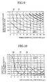
- Figs. 9 and 10 show calculation results, as similarly to Figs. 7 and 8, when both the normalized thickness (d1/h) of the top electrode 5 and the normalized thickness (d2/h) of the bottom electrode 3 are 0.1.
- the top electrode 5 and bottom electrode 3 are relatively thicker as compared to those of Figs. 7 and 8; therefor, comparing Fig. 7 with Fig. 9, the resonant frequency Fr of Fig. 9 is lower than that of Fig. 7 with respect to the same normalized SiO 2 thickness; and comparing Fig. 8 and Fig. 10, the normalized SiO 2 thickness of Fig. 10, such that the electromechanical coefficients k 2 of the second mode (TE2) and third mode (TE3) in Fig. 10 each are maximum, is larger than that of Fig. 8.
- the thickness g of the dielectric film 21 is not only simply affected by the resonant frequency Fr, but also largely affected by the electromechanical coefficient k 2 which has a large effect on the film bulk acoustic wave device. Further, as is apparent from Fig. 4, even in a case where the first mode (TE1) of the thickness extension vibration exhibits the characteristics of a high range cut-off or backward-wave type such that the frequency is lowered as the normalized piezoelectric film thickness is increased, the second mode (TE2) of the thickness extension vibration exhibits the characteristics of a low range cut-off.
- the electromechanical coefficient k 2 is the largest and an energy trapping possible film bulk acoustic wave device may be achieved.
- the electromechanical coupling coefficient k 2 of the second mode (TE2) is smaller by about 30 % than the maximum value of the first mode (TE1), the value of about 13 % of the maximum value, however, may be expected, and is larger as compared to a case of this type of the conventional film bulk acoustic wave device, thereby performing a film bulk acoustic wave device having the characteristics of wider band and lower loss.
- This is similarly applied even in a case of the third mode (TE3) or more, which the degree of modes to be used may be determined based on the frequency and electromechanical coupling coefficient k 2 to be required as a film bulk acoustic device.
- Fig. 11 shows a relationship between the normalized thickness of the top electrode 5 and normalized SiO 2 thickness so that the electromechanical coefficient k 2 can satisfy a certain condition.
- the horizontal axis of Fig. 11 represents a normalized thickness of the top electrode 5 or normalized electrode thickness (d1/h), and the vertical axis represents a normalized SiO 2 thickness (g/h).
- reference numeral 27 denotes a normalized SiO 2 thickness so that the first mode (TE1) can be equal in the electromechanical coefficient k 2 to the second mode (TE2); 28 denotes a normalized SiO 2 thickness so that the electromechanical coefficient k 2 of the second mode (TE2) can be the largest; 29 denotes a normalized SiO 2 thickness so that the second mode (TE2) can be equal in the electromechanical coefficient k 2 to the third mode (TE3); and 30 denotes a normalized SiO 2 thickness so that the electromechanical coefficient k 2 to the third mode (TE3) can be the largest.
- the normalized SiO 2 thickness is 3 or more, or the thickness g of the dielectric film 21 is set to 1.5 times the thickness 2h of the piezoelectric film 17, it can be brought to more than the normalized SiO 2 thickness 28 such that the electromechanical coefficient k 2 of the second mode (TE2) is maximum.
- the thickness g of the dielectric film 21 is set to 1.5 times or more the thickness 2h of the piezoelectric film 17, the effective electromechanical coefficient k 2 is larger than this type of the conventional film bulk acoustic wave device, thereby having the characteristics of wider band and lower loss, and performing an energy trapping possible film bulk acoustic wave device.
- the film bulk acoustic wave device when the film bulk acoustic wave device is produced so that the electromechanical coupling coefficient k 2 of the second mode (TE2) of the thickness extension vibration is the largest, an energy trapping possible film bulk acoustic wave device with desired favorable characteristics may be achieved.
- the basic structure of a film bulk acoustic wave device according to an embodiment 2 is the same as that shown in Figs. 5 and 6.
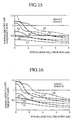
- Figs. 12 to 15 are graphs showing the characteristics of the film bulk acoustic wave device according to Embodiment 2.
- these designate the characteristics in which a top electrode 5 and a bottom electrode 3 are composed of platinum, a piezoelectric film 17 is composed of lead titanate, and a dielectric film 21 is composed of silicon oxide.
- the horizontal axis of Figs. 12 to 15 designates a normalized SiO 2 thickness (g/h), and the vertical axis thereof designates a normalized cut-off frequency (fc/f 0 ) in which a cut-off frequency fc is normalized by a resonant frequency f 0 of thickness resonance when the two sides are free surfaces.
- the cut-off frequency fc is almost the same as the resonant frequency in which the thickness resonance occurs.
- Fig. 12 is the calculation results in which both the normalized thickness (d1/h) of the top electrode 5 and the normalized thickness (d2/h) of the bottom electrode 3 are 0.1.
- Fig. 13 is the calculation results in which both the normalized thickness (d1/h) of the top electrode 5 and the normalized thickness (d2/h) of the bottom electrode 3 are 0.2.
- Fig. 14 is the calculation results in which both the normalized thickness (d1/h) of the top electrode 5 and the normalized thickness (d2/h) of the bottom electrode 3 are 0.3.
- Fig. 15 is the calculation results in which both the normalized thickness (d1/h) of the top electrode 5 and the normalized thickness (d2/h) of the bottom electrode 3 are 0.4.
- reference numeral 31 represents the characteristics of the first mode (TS1) of the thickness shear vibration
- 32 represents the characteristics of the second mode (TS2) of the thickness shear vibration
- 33 represents the characteristics of the third mode (TS3) of the thickness shear vibration
- 34 represents the characteristics of the fourth mode (TS4) of the thickness shear vibration
- 35 represents the characteristics of the first mode (TE1) of the thickness extension vibration
- 36 represents the characteristics of the second mode (TE2) of the thickness extension vibration.
- the normalized cut-off frequencies are respectively decreased for the above-mentioned modes.
- the normalized cut-off frequencies are respectively decreased for the above-mentioned modes.
- the normalized cut-off frequency of the TE1 mode is 0.719; however, when the normalized SiO 2 thickness is 4.0, the normalized cut-off frequency of the TE1 mode is lowered to 0.348.
- the dimensional relationship of the normalized cut-off frequency between the different modes is not regularly the same, it may vary depending on the normalized SiO 2 thickness.
- the dimensional relationship between the TE2 mode and the TS3 mode is important since it affects largely to the characteristics of the film bulk acoustic wave device.
- the normalized cut-off frequency of the TE2 mode when the normalized SiO 2 thickness is about 1.7 or less, the normalized cut-off frequency of the TE2 mode is larger than that of the TS3 mode. However, when the normalized SiO 2 thickness is laid between about 1.7 and about 3.4, the normalized cut-off frequency of the TE2 mode is smaller than that of the TS3 mode. When the normalized SiO 2 thickness is about 3.4 or more, the normalized cut-off frequency of the TE2 mode is larger than that of the TS3 mode.
- a range of the normalized SiO 2 thickness so that the normalized cut-off frequency of the TE2 mode can be smaller than that of the TS3 mode is about 1.9 to about 4.2 in Fig. 13, about 2.1 to about 4.8 in Fig. 14, and about 2.2 to about 5.3 in Fig. 15.
- Fig. 16 shows the calculation results in which the normalized thickness (d1/h) of the top electrode 5 is 0.1 and the normalized thickness (d2/h) of the bottom electrode 3 is 0.33.
- Fig. 17 shows the calculation results in which the normalized thickness (d1/h) of the top electrode 5 is 0.2 and the normalized thickness (d2/h) of the bottom electrode 3 is 0.33.
- Fig. 18 shows the calculation results in which the normalized thickness (d1/h) of the top electrode 5 is 0.3 and the normalized thickness (d2/h) of the bottom electrode 3 is 0.33.
- a range of the normalized SiO 2 thickness so that the normalized cut-off frequency of the TE2 mode can be smaller than that of the TS3 mode is determined, it is about 1.8 to about 4.2 in Fig. 16, about 2.0 to about 4.5 in Fig. 17, and about 2.1 to about 4.1 in Fig. 18.
- Fig. 19 is a graph showing the dispersion characteristics of the film bulk acoustic wave device according to the embodiment 2. This indicates the dispersion characteristics in which the top electrode 5 and bottom electrode 3 are composed of platinum, the piezoelectric film 17 is composed of lead titanate, and the dielectric film is composed of silicon oxide.
- the horizontal axis of Fig. 19 represents the normalized piezoelectric substance thickness (2kh) and the vertical axis thereof represents the normalized frequency (f/f 0 ), where f 0 is the same as those of Figs. 12 to 18.
- the normalized frequency at each mode in an intersection with the vertical axis is the normalized cut-off frequency (fc/f 0 ).
- Fig. 19 indicates the calculation results where the normalized thickness (d1/h) of the top electrode 5 is 0.2, the normalized thickness (d2/h) of the bottom electrode 3 is 0.33, and the normalized SiO 2 thickness (g/h) is 4.0, corresponding to the calculation results in a region where the normalized cut-off frequency of the TE2 mode in Fig. 17 is smaller than that of the TS3 mode.
- reference numeral 37 denotes a dispersion characteristic of the TS1 mode
- 38 denotes a dispersion characteristic of the TS2 mode
- 39 denotes a dispersion characteristic of the TS3 mode
- 40 denotes a dispersion characteristic of the TS4
- 41 denotes a dispersion characteristic of the TE1
- 42 denotes a dispersion characteristic of the TE2.
- the TE1 and TE2 modes denote backward-wave dispersion characteristics such that as the normalized piezoelectric substance thickness is larger, the normalized frequency is lowered in the vicinity of the vertical axis. This represents that a frequency range higher than the cut-off frequency corresponds to a cut-off mode incapable of propagating acoustic waves.
- Fig. 20 denotes the calculation results as well as Fig. 19 where the normalized SiO 2 thickness (g/h) is 6.0, and the calculation results in a region where the normalized cut-off frequency of the TE2 mode in Fig. 17 is larger than that of the TS3 mode.
- the TE1 mode denotes a backward-wave dispersion characteristic as well as Fig. 19, and the TE2 mode denotes a high-band-cut-off dispersion characteristic. Accordingly, in a case where the normalized SiO 2 thickness (g/h) is 6.0, when the second mode (TE2) of the thickness extension vibration is used, the energy of acoustic waves can be trapped, thereby obtaining a favorable film bulk acoustic wave device.
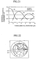
- Fig. 21 is a graph showing the characteristics of the film bulk acoustic wave device according to the embodiment 2. This indicates the characteristics where the top electrode 5 and bottom electrode 3 are composed of platinum, the piezoelectric film 17 is composed of lead titanate, and the dielectric film 21 is composed of silicon oxide.
- Fig. 21 is the calculation results where the normalized thickness (d1/h) of the top electrode 5 is 0.2, and the normalized thickness (d2/h) of the bottom electrode 3 is 0.33. These conditions are the same as those of Fig. 17.
- the horizontal axis of Fig. 17 corresponds to the normalized SiO 2 thickness (g/h), while the vertical axis corresponds to the effective electromechanical coupling coefficient k 2 .
- the effective electromechanical coupling coefficient k 2 of the TE2 mode is larger than those of the other modes, and is maximum around the normalized SiO 2 thickness of 4.5.
- the film bulk acoustic wave device using the TE2 mode was applied in a range that the effective electromechanical coupling coefficient k 2 had a large value.
- the normalized SiO 2 thickness is 4.5 or more, a favorable energy trapping possible film bulk acoustic wave device cannot be performed with the TE2 mode.
- Fig. 22 is a graph showing the measurement results of input impedance (S11) and output impedance (S22) of the film bulk acoustic wave device according to the embodiment 2, and represents the measurement results where the top electrode 5 and bottom electrode 3 is composed of platinum film using a titanium film as a contact film, the piezoelectric film 17 is composed of lead titanate, and the dielectric film 21 is composed of silicon oxide formed on a silicon nitride.
- the thickness of the titanium film constituting the top electrode 5 is 0.05 ⁇ m, and the thickness of the platinum film is 0.15 ⁇ m.
- the thickness of the titanium film constituting the bottom electrode 3 is 0.05 ⁇ m, and the thickness of the platinum film is 0.15 ⁇ m.
- the thickness 2h of the piezoelectric film 17 is 0.9 ⁇ m.
- the thickness of the silicon nitride constituting the dielectric film 21 is 0.1 ⁇ m, while the thickness of silicon oxide is 1.8 ⁇ m.
- the normalized thickness (d1/h) of the top electrode 5 and the normalized thickness (d2/h) of the bottom electrode 3 is about 0.33, while the normalized thickness (g/h) of the dielectric film 21 is 4.2.
- the dimensions of the input-side electrode 5a and output-side electrode 5b of the top electrode 4 is 14 ( ⁇ m) by 80 in rectangle, and the input-side electrode 5a is arranged apart from the output-side electrode 5b by 0.7 ⁇ m.
- a solid line 43 denotes the measurement results of the input impedance (S11); a dotted line 44 denotes the measurement results of the output impedance (S22).
- a solid line 45 denotes the measurement results of the loss
- a dotted line 46 denotes the measurement results of the phase.
- the characteristic around 800 MHz depends on the first mode (TE1) of the thickness extension vibration.
- the characteristic around 1.4 GHz depends on the second mode (TE2) of the thickness extension vibration. Since the thickness shear vibration little occurs in case of the piezoelectric film 17 composed of lead titanate, there is no appearance in the measurement results.
- TE1 of the thickness extension vibration as shown in Fig. 22, a large resonant circle is appeared in the impedance characteristics; as shown in Fig. 23, a transmission range is also present.
- the second mode (TE2) of the thickness extension vibration as shown in Fig. 22, a large resonant circle is appeared in the impedance characteristics; however, as shown in Fig. 23, the transmission range is extremely small.
- Figs. 24 and 25 denote the measurement results when the thickness of the silicon oxide is 2.0 ⁇ m, as well as Figs. 22 and 23. Accordingly, the normalized thickness (d1/h) of the top electrode 5 and the normalized thickness (d2/h) of the bottom electrode 3 are about 0.33, and the normalized thickness (g/h) of the dielectric film 21 is 4.7. In addition, the dimension of the input-side electrode 5a and output-side electrode 5b of the top electrode 5 is 14 ( ⁇ m) by 70 in rectangle. The input-side electrode 5a is arranged apart from the output-side electrode 5b by 0.5 ⁇ m.
- Fig. 22 is almost the same as Fig. 24, while in the transmission characteristics, Fig. 23 is different from Fig. 25.
- the normalized electrode thickness used for the measurements of Figs. 22 to 25 is close to the case of Fig. 13.
- the case of Figs. 22 and 23 is 4.2, while the case of Figs. 24 and 25 is 4.7; the energy-trapping is insufficient in both the cases.
- the case of Figs. 24 and 25 is closer in the intersection between the TE2 and TS3 modes; the case of Figs. 22 and 23 is more insufficient in the energy-trapping than that of Figs. 24 and 25; it appears such a difference provides the difference in the transmission characteristics.
- Fig. 26 denotes the normalized SiO 2 thickness in which the TE2 mode intersects with the TS3 mode.
- the horizontal axis of Fig. 26 corresponds to the normalized thickness of the top electrode 5, or normalized electrode thickness (d1/h), while the vertical axis corresponds to the normalized SiO 2 thickness (g/h).
- the solid lines 47 and 48 denote the case in which the top electrode 5 is the same thickness as the bottom electrode 3; the dashed lines 49 and 50 each denote in a case where the normalized thickness (d2/h) of the bottom electrode 3 is 0.33, and different from the thickness (d1/h) of the top electrode 5.
- reference numeral 47 and 49 denote a larger one of the normalized SiO 2 thicknesses in which the TE2 mode intersects with the TS3 mode
- 48 and 50 denote a smaller one of the normalized SiO 2 thicknesses in which the TE2 mode intersects with the TS3 mode.
- the equivalent density may be determined separately for each metal film.
- top electrode 5 and bottom electrode 3 each are composed of a platinum film and a titanium film, and the titanium film and the platinum film constituting the top electrode 5 and bottom electrode 3 are 0.05 ⁇ m thick, and 0.15 ⁇ m thick, respectively
- R (4.58 x 0.05/0.45 + 21.62 ⁇ 0.15/0.45)
- ⁇ 2 15, where 4.58 is a density of titanium, and 21.62 is a density of platinum.
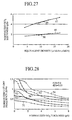
- Fig. 27 corresponds to a graph in which the horizontal axis of the graph shown in Fig. 26 is plotted as the equivalent density R.
- a locus where the top electrode 5 and bottom electrode 3 are different in thickness from each other matches a locus where they are equal in thickness to each other.
- the normalized SiO 2 thickness is larger than a locus representing a larger value of the normalized SiO 2 thicknesses in which the TE2 mode intersects with the TS3 mode.
- an approximate right line is determined from a locus exhibiting a larger value than the normalized SiO 2 thickness in which the TE2 mode crosses the TS3 mode in Fig.
- an energy trapping possible film bulk acoustic wave device may be achieved by use of the second mode (TE2) of the thickness extension vibration.
- the film bulk acoustic wave device has a larger electromechanical coefficient than this type of the conventional film bulk acoustic wave device, and little occurs the thickness shear vibration except the thickness extension vibration as a main vibration, thereby providing the characteristics of reduced losses or wider ranges as compared to the prior art.
- the top electrode 5 is composed of aluminum (Al) in Embodiment 3.
- the density of aluminum is 2690 (kg/m 3 ).
- Figs. 28 to 30 are graphs showing the characteristics of the film bulk acoustic wave device according to Embodiment 3. These here show the characteristics where the top electrode 5 is composed of aluminum, the bottom electrode 3 is composed of platinum, the piezoelectric film 17 is composed of lead titanate (PbTiO 3 ), and the dielectric film 21 is composed of silicon oxide.
- the horizontal axis of Figs. 28 to 30 corresponds to the normalized SiO 2 thickness (g/h), and the vertical axis thereof corresponds to the normalized cut-off frequency (fc/f 0 ).
- Fig. 28 represents the calculation results in a where the normalized thickness of the top electrode 5 (d1/h) is 0.1, and the normalized thickness (d2/h) of the bottom electrode 3 is 0.33.
- Fig. 29 represents the calculation results in a where the normalized thickness of the top electrode 5 (d1/h) is 0.2, and the normalized thickness (d2/h) of the bottom electrode 3 is 0.33.
- Fig. 30 represents the calculation results in a where the normalized thickness of the top electrode 5 (d1/h) is 0.3, and the normalized thickness (d2/h) of the bottom electrode 3 is 0.33.
- reference numeral 51 denotes the characteristics of the first mode (TS1) of the thickness shear vibration
- 52 denotes the characteristics of the second mode (TS2) of the thickness shear vibration
- 53 denotes the characteristics of the third mode (TS3) of the thickness shear vibration
- 54 denotes the characteristics of the fourth mode (TS4) of the thickness shear vibration
- 55 denotes the characteristics of the first mode (TE1) of the thickness extension vibration
- 56 denotes the characteristics of the second mode (TE2) of the thickness extension vibration.
- a dimensional relationship between the second mode (TE2) of the thickness extension vibration and the third mode (TS3) of the thickness shear vibration changes depending on the normalized SiO 2 thickness.
- Fig. 31 shows the normalized SiO 2 thickness in which the TS2 mode crosses the TS3 mode from the calculation results shown in Figs. 28 to 30.
- reference numerals 57 and 58 denoted by broken lines designate a case where the top electrode 5 is composed of aluminum.
- Fig 31 illustrates a locus where the top electrode 5 shown in Fig. 26 is composed of platinum.
- Fig. 32 designates where the graphs shown in Fig. 31 are plotted by the horizontal axis as the equivalent density R.
- a locus of the top electrode 5 composed of aluminum is different from one of the top electrode 5 composed of platinum. This reason is as follows: since the aluminum density is greatly different from the platinum density, a relationship between the contribution due to the mass load and the contribution due to the top electrode 5 thickness differs largely in a case where the top electrode 5 is composed of either aluminum or platinum. In a case where the top electrode 5 is composed of aluminum in Fig.
- an energy trapping possible film bulk acoustic wave device may be achieved by use of the second mode (TE2) of the thickness extension vibration.
- the film bulk acoustic wave device has a larger electromechanical coefficient than the conventional type film bulk acoustic wave device, and little occurs the thickness shear vibration except the thickness extension vibration as a main vibration, thereby providing the characteristics of reduced losses or wider ranges as compared to the prior art.
- the above-mentioned matter is applied similarly to a case where the top electrode 5 is composed of a titanium film formed on the piezoelectric film 17 and an aluminum film formed thereon.
- the thickness of the silicon oxide to perform the energy entrapping possible film bulk acoustic wave device with the second mode (TE2) of the thickness extension vibration, as described in above, varies depending on the velocity of acoustic waves that propagates in an actual silicon oxide.
- Fig. 33 shows the calculation results as well as Fig. 29 in a case where the acoustic constant c of the silicon oxide is multiplied by 0.9.
- the propagation velocity is decrease by about 5 %.
- the normalized SiO 2 thicknesses in which the second mode (TE2) of the thickness extension vibration crosses the third mode (TS3) of the thickness shear vibration are 1.60 and 3.65, which are smaller by 4-5 % as compared to the case of Fig. 29.
- Fig. 34 shows the calculation results as well as Fig. 29 in a case where the density p of the silicon oxide is multiplied by 1.1. Also when the density ⁇ of the silicon oxide is multiplied by 1.1, the velocity V is smaller by about 5 %.
- the normalized SiO 2 thicknesses in which the second mode (TE2) of the thickness extension vibration crosses the third mode (TS3) of the thickness shear vibration are 1.63 and 3.66, which are smaller by about 4 %.
- the bottom electrode 3 is composed of iridium (Ir) in Embodiment 4.
- the density of aluminum is 22500 (kg/m 3 ).
- the piezoelectric film 17 is composed of lead titanate
- the iridium film is especially applied to the bottom electrode 3, thus performing a lead titanate film with an extremely favorable crystallinity.
- the density of iridium is 22400 (kg/m 3 ), and extremely close to the density of platinum (21370 (kg/m 3 )).
- the locus of the normalized SiO 2 thicknesses in which the TE2 mode crosses the TS3 mode is found, it approximates to the loci of the solid lines 47 and 48 in Fig. 32. Therefore, in a case where the bottom electrode 3 is composed of iridium, and the top electrode 5 is composed of platinum, the normalized SiO 2 thickness (g/h) is set to (0.147 ⁇ R + 2.85) or more, thereby resulting in the same effect as Embodiment 2.
- the above-mentioned matter is applied similarly to a case where the bottom electrode 3 is composed of a titanium film formed on the titanium film 21 and an iridium film formed thereon.
- the top electrode 5 is composed of aluminum in Embodiment 5 and the bottom electrode 3 is composed of iridium.
- the aluminum density is 22500 (kg/m 3 ), and close to the platinum density: 21370 (kg/m 3 ).
- the locus of the normalized SiO 2 thicknesses in which the TE2 mode crosses the TS3 mode is found, it approximates to the loci of the solid lines 57 and 58 in Fig. 32. Therefore, in a case where the bottom electrode 3 is composed of iridium, and the top electrode 5 is composed of platinum, the normalized SiO 2 thickness (g/h) is set to (0.147 ⁇ R + 2.85) or more, thereby resulting in the same effect as Embodiment 3.
- the piezoelectric film 17 is composed of lead titanate-zirconate (PZT) in Embodiment 6.
- the characteristics of PZT is similar to those of lead titanate, and a film bulk acoustic wave device having a piezoelectric film 16 composed of lead titanate-zirconate exhibits the same characteristics as those of Figs. 12 to 18.
- the piezoelectric film 17 is composed of lead titanate-zirconate
- the normalized SiO 2 thickness (g/h) is set to (0.147 ⁇ R + 2.85) or more, thereby resulting in the same effect as Embodiment 2.
- the normalized SiO 2 thickness (g/h) is set to (0.034 ⁇ R + 3.57) or more, thereby resulting in the same effect as Embodiment 2.
- Figs. 35 and 36 are views showing a film bulk acoustic wave device according to Embodiment 7 of this invention.
- Fig. 35 is a top-side view
- Fig 36 is a cross sectional view taken along line III-III.
- reference numeral 17 denotes a piezoelectric film composed of lead titanate-zirconate
- 59 denotes a first silicon oxide formed on the silicon nitride 16
- 60 denotes a second silicon film formed on the top electrode 5.
- the same reference numerals are denoted with the same components as Figs. 1 and 2.
- This embodiment includes the first silicon oxide 59 formed on the silicon nitride 16 and the second silicon oxide 60 formed on the top electrode 5.
- the thickness resonance occurs between the bottom surface of the silicon nitride 16 and the top surface of the second silicon film 60.
- the resonant frequency here may be found by the same calculation method as the case described in the aforementioned embodiment. That is, since it is assumed that the silicon oxide of a single layer is divided into two layers, an energy trapping possible film bulk acoustic wave device may be performed, e.g., without an operation to add an addition to lead titanate-zirconate.
- a fine adjustment for the thickness of the second silicon oxide 60 may contribute to adjust the errors in thickness upon fabrications, and simultaneously, to function effectively as a protective film, for example, in a case where the top electrode 5 is formed by a material with a poor corrosion resistance as compared to gold and platinum.
- the same effect may be obtained even in a case where it is composed of lithium tantalate. Further, in a piezoelectric film composed of a material having a one-third (0.33) or less in the Poisson's ratio and having a thickness extension vibration as a main vibration, the same effect may be also obtained.
- the top electrode 5 and bottom electrode 3 is composed of a material such as platinum, iridium, aluminum.
- the normalized SiO 2 thickness (g/h) is set to (0.147 ⁇ R + 2.85) or more, thereby resulting in the same effect as Embodiment 2.
- the normalized SiO 2 thickness (g/h) is set to (0.023 ⁇ R + 3.57) or more, thereby resulting in the same effect as Embodiment 3.
- the top electrode 5 is formed by separating the input-side electrode 5a from the output-side electrode 5b in the aforementioned embodiment, a single case is also possible.
- the lead titanate is referred to the literature: "Neue Serie, ed.: Landolt-bornstein, pp.80, Springer-Verlag, Berlin, 1981", while the other are referred to the literatures: B. A. Auld, "Acoustic Fields and Waves in Solids", vol.I, pp.357-382, A Wiley-Interscience Publication, John Wiley & Sons, and National Astronomy Observatory, ed.: Science Chronological Table, 1997, pp. Phy/19(438), pp. Phy/26(446)-27(447).
- an appropriate SiO 2 thickness may be determined by a conversion based on a ratio between the literature value and the constant of actual materials.
- the mass represented as the normalized SiO 2 thickness may be not necessarily limited by silicon oxide if it is a dielectric, and silicon oxide may include SiO, not actually not genuine SiO 2 .
- the film bulk acoustic wave device is adapted to prevent the breakdown of components on the etching to form a via hole, and simultaneously prevent the deterioration of the characteristics of the components due to the inner stress upon formation of the via hole.
- the film bulk acoustic wave device is adapted to perform the characteristics of reduced losses and wider ranges.
Landscapes
- Physics & Mathematics (AREA)
- Acoustics & Sound (AREA)
- Engineering & Computer Science (AREA)
- Chemical & Material Sciences (AREA)
- Ceramic Engineering (AREA)
- Manufacturing & Machinery (AREA)
- Piezo-Electric Or Mechanical Vibrators, Or Delay Or Filter Circuits (AREA)
- Surface Acoustic Wave Elements And Circuit Networks Thereof (AREA)
Abstract
There is provided a film bulk acoustic wave device
comprising: a silicon substrate 1, a dielectric film 21
including a silicon nitride 16 formed on the substrate 1 and
a silicon oxide 2 on the silicon nitride 16, a bottom electrode
3 formed on the dielectric film 21, a piezoelectric film 17
formed on the bottom electrode 3, and a top electrode 5 formed
on the piezoelectric film 17, wherein a via hole is formed in
such a manner that the thickness direction of a part of the
silicon substrate 1 which is opposite to a region including a
part where the top electrode 5 exists is removed from the bottom
surface of the silicon substrate 1 to a boundary surface with
the silicon nitride 16.
Description
The present invention relates to a film bulk acoustic
device using an acoustic wave such as resonators and filters.
Figs. 1 and 2 show this type of the conventional film bulk
acoustic wave device as described in, for example, the
literature "Bulk-Acoustic-Wave Devices using the Second-Order
Thickness-Extensional Mode in Thin ZnO-SiO2 Composite Films on
Si", Proceedings of The Acoustical Society of Japan, pp. 691-692,
Sept.-Oct. 1985 (hereinafter, referred to as reference 1), and
the literature "Fundamental Bulk Acoustic Resonators in GHz
Range", Proceedings of The Institutes of Electronics,
Information and Communication Engineers, vol.81, No.5,
pp.468-472, 1998 (hereinafter, referred to as reference 2).
Fig. 1 is a top view, and Fig. 2 is a cross sectional view taken
along line I-I in Fig. 1. In the figures, reference numeral
1 denotes a silicon (Si) substrate; 2 denotes a silicon oxide
(SiO2) formed on the silicon substrate 1; 3 denotes a bottom
electrode formed on the silicon oxide 2; 4 denotes a
piezoelectric film composed of zinc oxide (ZnO) formed on the
bottom electrode 3; 5 denotes a top electrode, divided into
input-side electrode 5a and output-side electrode 5b, formed
on the piezoelectric film 4; and 6 denotes a via hole.
When a voltage is applied to the top electrode 5 and the
bottom electrode 3, an electric field is generated in the
piezoelectric film 4. At this time, an acoustic distortion in
the piezoelectric film 4 is caused by the electric field. When
the applied voltage is a signal of frequency f, this distortion
also vibrates at the same frequency f and excites an acoustic
wave. In the case of a structure as shown in Figs. 1 and 2,
the excited acoustic wave propagates in the thickness direction,
and the acoustic wave propagated in the thickness direction is
reflected on the respective air-contact surfaces on the surface
of the top electrode 5 and the lower surface of the silicon oxide
2. Therefor, there occurs an acoustic resonance when a gap
between the surface of the top electrode 5 and the lower surface
of the silicon oxide film 2 is an integer multiple of the half
wave length of the acoustic wave.
On the other hand, there also occurs the propagation of
the acoustic wave in the direction parallel to the surface in
the interior of the piezoelectric film. The acoustic wave in
the piezoelectric film 4 at this moment comes to be a cut-off
mode at a frequency lower than a certain frequency f0, and comes
to be a propagation mode at a frequency higher than the frequency
f0. The frequency f0 is a cut-off frequency, and corresponds
to a frequency in which the thickness 2h of the piezoelectric
film 4 coincides with a half wavelength of the acoustic wave
propagating in the thickness direction in the piezoelectric
film 4 when the two surfaces of the piezoelectric film 4 are
free surfaces.
In the case of the electrode unit in which the top
electrode 5 is present on the surface, the cut-off frequency
fm0 of the electrode unit is lower than the cut-off frequency
ff0 of a non-electrode unit provided with only the bottom
electrode 3, due to the electrode thickness and mass load.
Therefor, in the range of the frequencies ff0 to fm0, the acoustic
wave is the propagation mode due to a higher frequency side than
the cut-off frequency fm0 in the electrode unit, while it is
the cut-off mode due to a lower frequency side than the cut-off
frequency ff0 in the non-electrode unit. Hence, the acoustic
wave propagating in parallel to the surface of the film 4 results
in a state that an energy is trapped in the top electrode 5.
When the input-side electrode 5a and output-side
electrode 5b of the top electrode 5 are set appropriately at
a symmetric mode frequency providing the common potential, and
at an asymmetric mode frequency providing potentials different
from each other, an electric signal applied to the input-side
electrode 5a is traveled to the output-side electrode 5b with
low loss. Thus, the pass band of a filter is created.
The characteristics of such a filter are determined by
the thickness 2h of the piezoelectric film 4, the thickness of
the top electrode 5, the thickness g of the silicon oxide 2,
the shape of the top electrode 5, and a gap between the input-side
electrode 5a and the output-side electrode 5b.
The reference 1 describes one example in which a
normalized thickness (g/h) of the piezoelectric film 4 is 1.54
and 2.4, which is determined by the thickness 2h of the
piezoelectric film 4 and the thickness g of the silicon oxide
2. The reference 1 also represents that the design is made by
focusing the temperature characteristics and the loss of the
acoustic wave. In addition, the reference 1 designates to use
an acoustic wave of the second mode. The acoustic wave is a
fundamental mode (first mode) when a gap between the surface
of the top electrode 5 and the back of the silicon oxide 2 is
a half wave length of the acoustic wave, and an N-th mode (N:
integer) corresponds to an N multiple of the wave length of the
fundamental mode.
Fig. 3 shows this type of the conventional film bulk
acoustic device described in, for example, JP-A 6-350154
(hereinafter, referred to as reference 3). Fig. 3 is a cross
sectional view. Though the basic structure is the same as that
shown in Fig. 2, a piezoelectric film 7 is composed of lead
titanate-zirconate (PZT); a bottom electrode 3 is composed of
a titanium (Ti) film 8 and a platinum (Pt) film 9; and a top
electrode 5 is composed of a titanium film 10 and a gold (Au)
film 11.
The reference 3 describes one example in which a
normalized thickness (d/h) of the bottom electrode 3 is 1.0,
which is determined by the thickness 2h of the piezoelectric
film 7 and the thickness d of the bottom electrode 3. In
addition, the reference 3 designates that favorable
piezoelectric characteristics may be performed by an
appropriate composition ratio of lead titanate (PbTiO3) and lead
zirconate (PbZrO3).
The piezoelectric film 7 composed of lead titanate-zirconate
excites a thickness extension vibration as a main
vibration. In this case, the acoustic wave propagating in
parallel with the surface of the piezoelectric film 7 designates
the dispersion characteristics as shown in Fig. 4. In Fig. 4,
the horizontal axis corresponds to a normalized thickness of
the piezoelectric film 7 which multiplies the wave number k of
the acoustic wave propagating in parallel with the surface of
the film 7, and the thickness of the piezoelectric film 7
together, that is, a normalized piezoelectric thickness (2kh),
while the vertical axis corresponds to a frequency.
In the figure, reference numeral 12 designates the
characteristics of a first mode (TE1) of the thickness extension
vibration; 13 designates the characteristics of a second mode
(TS2) of the thickness shear vibration; 14 designates the
characteristics of a third mode (TS3) of the thickness shear
vibration; and 15 designates the characteristics of a second
mode (TE2) of the thickness extension vibration. A range that
the normalized piezoelectric substance thickness is a real
number is a range that the acoustic wave is a propagation mode,
while a range that the normalized piezoelectric substance
thickness is an imaginary number is a range that the acoustic
wave is a cut-off mode. In addition, the frequency at the
crossing point with the vertical axis, such that the normalized
thickness is zero, is a cut-off frequency f0.
As is apparent from Fig. 4, the first mode (TE1) of the
thickness extension vibration shows a characteristic that the
frequency is made lower as the normalized piezoelectric
substance thickness is larger in the vicinity of the vertical
axis. In addition to lead zirconate titanate, this is also
applied similarly in a piezoelectric film having the thickness
extension vibration as a main vibration, constituting lead
titanate (PbTiO3), lithium tantalate (LiTaO3), or a material
having the Poisson's ratio of one-third or less.
When a characteristic like the first mode (TE1) of the
thickness extension vibration in Fig. 4 is exhibited, the
cut-off mode corresponds to a frequency higher than the cut-off
frequency fm0 in a range that the top electrode 5 exists, while
the propagation mode corresponds to a frequency lower than the
cut-off frequency ff0 in a range that the top electrode 5 is
absent. Therefor, a favorable energy trapping cannot be
performed, resulting in enlarged loss. The variations of the
characteristics of the filter may be enlarged under the
influence of the ambience of the top electrode 5.
As a method to prevent such a drawback, a method as
described in JP-B 58/58828 (hereinafter, referred to as
reference 4) has been used. That is, an addition is added to
lead titanate-zirconate, so that the Poisson's ratio of the lead
titanate-zirconate mixed with the addition can be one-third or
more. Instead of the characteristics like the first mode (TE1)
of the thickness extension vibration in Fig. 4, it is set to
show up the following characteristics: the frequency is higher
as the thickness of the normalized piezoelectric substance is
larger in the vicinity of the vertical axis, thereby performing
the same energy trapping as a case where the piezoelectric film
4 composed of lead oxide are applied. Note that when the
Poisson's ratio exceeds one-third, the cut-off frequency of the
first mode (TE1) of the thickness extension vibration is higher
than that of the second mode (TS2) of the thickness shear
vibration.
This type of the conventional film bulk acoustic wave
device which enables to perform the energy trapping is limited
by a piezoelectric film composed of a material such as zinc oxide
which generates the thickness shear vibration as a main
vibration. For this reason, there is a drawback such that it
is difficult to flexibly correspond to a variety of
characteristics necessary for a filter.
In the piezoelectric film composed of a material such as
lead titanate-zirconate, having the thickness extension
vibration as a main vibration, since it is difficult to perform
the energy-trapping as it stands, the energy-trapping has been
performed by bringing the Poisson's ratio to one-third or more
with mixing an addition to the material. But, the method
described in the reference 4 can be performed only by a
fabrication method which sinters piezoelectric ceramics. When
the method is applied to a piezoelectric film, it is difficult
to maintain favorably the quality of the piezoelectric film,
resulting in deteriorating the characteristics of film bulk
acoustic wave devices.
The present invention has been made to solve the
aforementioned drawbacks, and an object of this invention is
to obtain a film bulk acoustic wave device which enables an
energy trapping with a piezoelectric film for exciting or
generating a thickness extension vibration as a main vibration,
thereby providing a more favorable characteristic than the
prior art.
A film bulk acoustic wave device according to the present
invention comprises: a substrate; a dielectric film including
a silicon nitride (SiN) formed on the substrate and a silicon
oxide (SiO2) on the silicon nitride; a bottom electrode formed
on the dielectric film; a piezoelectric film formed on the
bottom electrode; and a top electrode formed on the
piezoelectric film, wherein a via hole is formed in such a manner
that the thickness direction of a part of the substrate which
is opposite to a region including a part where the top electrode
exists is removed from the bottom surface of the substrate to
a boundary surface with the silicon nitride.
Thus, the breakdown of the components upon the etching
to form a via hole may be prevented through the silicon nitride,
and simultaneously, the inferiority of the characteristics of
the components due to the deformation caused by the inner stress
upon forming the via hole may be prevented.
In the film bulk acoustic wave device according to this
invention, the silicon oxide is formed separately on the silicon
nitride and on the top electrode.
Thus, the errors on fabrication may be adjusted by the
silicon oxide formed on the top electrode, and simultaneously,
the top electrode may be protected.
In the film bulk acoustic wave device according to this
invention, the piezoelectric film generates a thickness
extension vibration as a main vibration, and in order to prevent
the thickness of the silicon nitride from affecting the
vibration characteristics, the thickness of the silicon oxide
is larger than that of the silicon nitride, and 1.5 times or
more the thickness of the piezoelectric film.
Thus, an energy trapping possible film bulk acoustic wave
device may be performed, which has an effective
electromechanical coupling coefficient k2 larger than this type
of the conventional film bulk acoustic wave device and has the
characteristics of wider range and reduced loss, thereby
preventing unnecessary spurious occurrences caused by the end
shape of the piezoelectric substance originally irrelevant to
the characteristics of the film bulk acoustic wave device, a
positional relationship between the end of the piezoelectric
substance and the end of the via hole, and so on, and further
preventing enlarged loss when the energy of an acoustic wave
propagates to the outside of the top electrode.
A film bulk acoustic wave device according to this
invention comprises: a dielectric film; a bottom electrode
including a conductor having a density of 10000 (kg/m3) or more;
a piezoelectric film which generates a thickness extension
vibration as a main vibration; and a top electrode including
a conductor having a density of 10000 (kg/m3) or more, wherein
when the thickness of the piezoelectric film is set to 2h, the
thickness of the dielectric film is set to g, the density of
the top electrode is set to ρ1 × 1000 (kg/m3), the thickness
of the top electrode is set to d1, the density of the bottom
electrode is set to ρ2 × 1000 (kg/m3), the thickness of the
bottom electrode is set to d2, and an equivalent density R is
set to R = (ρ1d1/h) + (ρ2d2/h), the normalized thickness (g/h)
of the dielectric film determined by the thicknesses of the
piezoelectric film and the dielectric film is {0.15 × R + 2.8}
or more.
Thus, the film bulk acoustic wave device may perform an
energy trapping by use of the second mode (TE2) of the thickness
extension vibration, and further has a larger electromechanical
coupling coefficient than this type of the conventional film
bulk acoustic wave device and little occurs a thickness shear
vibration other than the thickness extension vibration as a main
vibration, thereby achieving the characteristics of a wider
range and a lower loss than the prior art.
A film bulk acoustic wave device according to this
invention comprises: a dielectric film; a bottom electrode
including a conductor having a density of 10000 (kg/m3) or more;
a piezoelectric film which generates a thickness extension
vibration as a main vibration; and a bottom electrode including
a conductor having a density of 10000 (kg/m3) or less, wherein
when the thickness of the piezoelectric film is set to 2h, the
thickness of the dielectric film is set to g, the density of
the top electrode is set to ρ1 × 1000 (kg/m3), the thickness
of the top electrode is set to d1, the density of the bottom
electrode is set to ρ2 × 1000 (kg/m3), the thickness of the
bottom electrode is set to d2, and an equivalent density R is
set to R = (ρ1d1/h) + (ρ2d2/h), the normalized thickness (g/h)
of the dielectric film determined by the thicknesses of the
piezoelectric film and the dielectric film is {0.023 × R + 3.5}
or more.
Thus, the film bulk acoustic wave device may perform an
energy trapping by use of the second mode (TE2) of the thickness
extension vibration, and further has a larger electromechanical
coupling coefficient than this type of the conventional film
bulk acoustic wave device and little occurs a thickness shear
vibration other than the thickness extension vibration as a main
vibration, thereby achieving the characteristics of a wider
range and a lower loss than the prior art.
In the film bulk acoustic wave device according to this
invention, the dielectric film has a silicon nitride (SiN)
formed on the substrate, and a via hole is formed in such a manner
that the thickness direction of a part of the substrate which
is opposite to a region including a part where the top electrode
exists is removed from the bottom surface of the substrate to
a boundary surface with the silicon nitride.
Thus, the breakdown of the components upon the etching
to form a via hole may be prevented through the silicon nitride,
and simultaneously, the inferiority of the characteristics of
the components due to the deformation caused by the inner stress
upon forming the via hole may be prevented.
In the film bulk acoustic wave device according to this
invention, the silicon oxide is formed separately on the
substrate and on the top electrode.
Thus, the error of the thickness upon fabrication may be
adjusted and simultaneously, the top electrode may be
protected.
In the film bulk acoustic wave device according to this
invention, the bottom electrode is mainly composed of either
platinum (Pt) or iridium (Ir).
Thus, a favorable piezoelectric film may be obtained.
In the film bulk acoustic wave device according to this
invention, the piezoelectric film has as a main component either
one of lead titanate (PbTiO3), lead titanate-zirconate (PZT),
lithium tantalate (LiTaO3), and a material having the Poisson's
ratio less than 0.33.
Thus, a flexible countermeasure may be performed in
accordance with the characteristics required for the film bulk
acoustic wave device.
Fig. 1 is a top view showing a conventional film bulk
acoustic wave device having a piezoelectric film composed of
zinc oxide.
Fig. 2 is a cross sectional view showing the conventional
film bulk acoustic wave device having a piezoelectric film
composed of zinc oxide.
Fig. 3 is a cross sectional view showing a conventional
film bulk acoustic wave device having a piezoelectric film
composed of PZT.
Fig. 4 is a graph showing dispersion characteristics of
the conventional film bulk acoustic wave device having a
piezoelectric film composed of PZT.
Fig. 5 is a top view showing a film bulk acoustic wave
device according to Embodiment 1 of the present invention.
Fig. 6 is a cross sectional view showing the film bulk
acoustic wave device according to Embodiment 1 of this
invention.
Fig. 7 is a graph showing the normalized resonant
frequency characteristics (d1/h = 0.02, d2/h = 0.02) of the film
bulk acoustic wave device according to Embodiment 1 of this
invention.
Fig. 8 is a graph showing the electromechanical coupling
coefficient characteristics (d1/h = 0.02, d2/h = 0.02)
according to Embodiment 1 of this invention.
Fig. 9 is a graph showing the normalized resonant
frequency characteristics (d1/h = 0.1, d2/h = 0.1) of the film
bulk acoustic wave device according to Embodiment 1 of this
invention.
Fig. 10 is a graph showing the electromechanical coupling
coefficient characteristics (d1/h = 0.1, d2/h = 0.1) of the film
bulk acoustic wave device according to Embodiment 1 of this
invention.
Fig. 11 is a graph showing a relationship between the
normalized thickness of the top electrode and the normalized
SiO2 thickness when the electromechanical coupling coefficient
k2 satisfies a certain condition.
Fig. 12 is a graph showing the normalized cut-off
frequency characteristics (d1/h = 0.1, d2/h = 0.1) of the film
bulk acoustic wave device according to Embodiment 2 of this
invention.
Fig. 13 is a graph showing the cut-off frequency
characteristics (d1/h = 0.2, d2/h = 0.2) of the film bulk
acoustic wave device according to Embodiment 2 of this
invention.
Fig. 14 is a graph showing the normalized cut-off
frequency characteristics (d1/h = 0.3, d2/h = 0.3) of the film
bulk acoustic wave device according to Embodiment 2 of this
invention.
Fig. 15 is a graph showing the normalized cut-off
frequency characteristics (d1/h = 0.4, d2/h = 0.4) of the film
bulk acoustic wave device according to Embodiment 2 of this
invention.
Fig. 16 is a graph showing the normalized cut-off
frequency characteristics (d1/h = 0.1, d2/h = 0.33) of the film
bulk acoustic wave device according to Embodiment 2 of this
invention.
Fig. 17 is a graph showing the normalized cut-off
frequency characteristics (d1/h = 0.2, d2/h = 0.33) of the film
bulk acoustic wave device according to Embodiment 2 of this
invention.
Fig. 18 is a graph showing the normalized cut-off
frequency characteristics (d1/h = 0.3, d2/h = 0.33) of the film
bulk acoustic wave device according to Embodiment 2 of this
invention.
Fig. 19 is a graph showing the dispersion characteristics
(g/h = 4.0) of the film bulk acoustic wave device according to
Embodiment 2 of this invention.
Fig. 20 is a graph showing the dispersion characteristics
(g/h = 6.0) of the film bulk acoustic wave device according to Embodiment 2 of this invention.
Fig. 21 is a graph showing the electromechanical coupling
coefficient characteristics of the film bulk acoustic wave
device according to Embodiment 2 of this invention.
Fig. 22 is a graph showing the impedance characteristics
(g/h = 4.2) of the film bulk acoustic wave device according to
Embodiment 2 of this invention.
Fig. 23 is a graph showing the passing characteristics
(g/h = 4.2) of the film bulk acoustic wave device according to
Embodiment 2 of this invention.
Fig. 24 is a graph showing the impedance characteristics
(g/h = 4.7) of the film bulk acoustic wave device according to
Embodiment 2 of this invention.
Fig. 25 is a graph showing the passing characteristics
(g/h = 4.7) of the film bulk acoustic wave device according to
Embodiment 2 of this invention.
Fig. 26 is a graph showing the normalized SiO2 thickness
in which the TE2 mode crosses the TS3 mode of the film bulk
acoustic wave device according to Embodiment 2 of this invention
when the horizontal axis is designated as the normalized
electrode thickness.
Fig. 27 is a graph showing the normalized SiO2 thickness
in which the TE2 mode crosses the TS3 mode of the film bulk
acoustic wave device according to Embodiment 2 of this invention
when the horizontal axis is designated as the equivalent
density.
Fig. 28 is a graph showing the normalized cut-off
frequency characteristics (d1/h = 0.1, d2/h = 0.33) of the film
bulk acoustic wave device according to Embodiment 3 of this
invention.
Fig. 29 is a graph showing the normalized cut off
frequency characteristics (d1/h = 0.2, d2/h = 0.33) of the film
bulk acoustic wave device according to Embodiment 3 of this
invention.
Fig. 30 is a graph showing the normalized cut-off
frequency characteristics (d1/h = 0.3, d2/h = 0.33) of the film
bulk acoustic wave device according to Embodiment 3 of this
invention.
Fig. 31 is a graph showing the normalized SiO2 thickness
in which the TE2 mode crosses the TS3 mode of the film bulk
acoustic wave device according to Embodiment 3 of this invention
when the horizontal axis is designated as the normalized
electrode thickness.
Fig. 32 is a graph showing the normalized SiO2 thickness
in which the TE2 mode crosses the TS3 mode of the film bulk
acoustic wave device according to Embodiment 3 of this invention
when the horizontal axis is designated as the equivalent
density.
Fig. 33 is a graph showing the normalized cut-off
frequency characteristics of the film bulk acoustic wave device
according to Embodiment 3 of this invention when the acoustic
constant is varied.
Fig. 34 is a graph showing the normalized cut-off
frequency characteristics of the film bulk acoustic wave device
according to Embodiment 3 of this invention when the density
is varied.
Fig. 35 is a top view showing a film bulk acoustic wave
device according to Embodiment 7 of this invention.
Fig. 36 is a cross sectional view showing the film bulk
acoustic wave device according to Embodiment 7 of this
invention.
Fig. 37 is a cross sectional view showing a modification
of the film bulk acoustic wave device.
In order to describe the invention in greater detail, the
preferred embodiments of the invention will be described below
with reference to the accompanying figures.
Figs. 5 and 6 show a film bulk acoustic wave device 4
according to an embodiment 1 of the present invention. Fig.
5 is a top view; and Fig. 6 is a cross sectional view taken along
line II-II. In the figures, reference numeral 1 denotes a
silicon (Si) substrate; 21 denotes a dielectric film formed on
the silicon substrate 1, and composed of a silicon nitride (SiN)
16 formed on the silicon substrate 1 and a silicon oxide (SiO2)
2 formed thereon, in this embodiment. 3 denotes a bottom
electrode formed on the dielectric film 21, and composed of a
titanium (Ti) film formed on the silicon oxide 2 and a platinum
(Pt) film formed thereon, in this embodiment. 17 denotes a
piezoelectric film composed of lead titanate (PbTiO3). 5
denotes a top electrode formed on the piezoelectric film 17,
having the same structure as the bottom electrode 3 in this
embodiment. 18 denotes an air bridge and connects the top
electrode 5 to a bonding pad 19. 20 denotes a bonding pad which
connects the bottom electrode 3. Note that the same reference
numerals or symbols will be denoted by the same components as
those of Figs. 1 and 2. A via hole 6 is formed by removing the
bottom surface of the silicon substrate 1 to the boundary
surface of the silicon nitride 16 in the thickness direction
of a part of the silicon substrate 1 opposite to a region
including a part provided with the top electrode 5.
The silicon nitride 16 is particularly favorable in the
resistance to an etching solution so as to form the via hole
6 and in the characteristics to an inner stress for achievement
of a flat surface, and is particularly suitable for formation
of the surface in contact with the via hole 6. Hence, the
application of the silicon nitride 16 may prevent the breakdown
of elements during etching and also prevent the deterioration
of the characteristics of the elements due to the deformation
caused by the inner stress.
The titanium film of the bottom electrode 3 is inserted
for improvement of an adhesion between the platinum film formed
thereon and the dielectric film 21. In addition, the
crystallinity of the platinum film of the bottom electrode 3
is very important so as to obtain a favorable piezoelectric film
17 since the piezoelectric film 17 grows along the crystal
lattice of the platinum film. Note that the platinum film of
the top electrode 5 is used because of its relatively excellent
characteristics with respect to corrosion-resistance and
electrical resistance. For these purposes, since the platinum
and titanium films are applied to the top electrode 5 and bottom
electrode 3, the thickness of the platinum film is relatively
thicker than that of the titanium film. For example, it is
designated by a relationship of the platinum film: 0.1 µm thick
and the titanium film: 0.03 µm thick.
In the following description, the thickness of the
piezoelectric film 17 is set to 2h; the thickness of the top
electrode 5 is set to d1; the thickness of the bottom electrode
3 is set to d2; and the thickness of the dielectric film 21 is
set to g. However, the platinum film is thicker than the
titanium film, and further the density of platinum is 21370 kg/m3,
while the density of titanium is 4540 kg/m3. Thus, since the
platinum film affects more largely than the titanium film with
respect to the mass load, the thickness of the platinum film
is used as a central value when the thickness of the top electrode
5 is d1 and the thickness of the bottom electrode 3 is d2. On
the other hand, since there is no critical difference between
the silicon nitride 16 and the silicon oxide 2, the sum in
thickness of the silicon nitride 16 and the silicon oxide 2 is
used when the thickness of the dielectric film 21 is g.
Figs. 7 and 8 are graphs showing the characteristics of
the film bulk acoustic wave device according to Embodiment 1.
These show the characteristics when the top electrode 5 and
bottom electrode 3 are composed of platinum, the piezoelectric
film 17 is composed of lead titanate, and the dielectric film
21 is composed of silicon oxide. Figs. 7 and 8 show the
calculation results in a case where both the normalized
thickness d1/h of the top electrode 5 determined by the
thickness 2h of the piezoelectric film 17 and the thickness d1
of the top electrode 5, and the normalized thickness d2/h of
the bottom electrode 3 determined by the thickness 2h of the
piezoelectric film 17 and the thickness d2 of the bottom
electrode 3 is 0.02.
The horizontal axes in Figs. 7 and 8 are the normalized
thickness of the dielectric film 21, that is, normalized SiO2
thickness (g/h), determined by the thickness 2h of the
piezoelectric film 17 and the thickness g of the piezoelectric
film 21, that is, normalized SiO2 thickness (g/h). The vertical
axis in Fig. 7 is the normalized resonant frequency Fr/f0 when
the resonant frequency Fr of the electrode unit is normalized
by the resonant frequency f0 in thickness resonance when both
surfaces of the electrode unit are free surfaces. The vertical
axis in Fig. 8 is the effective electromechanical coefficient
k2 determined by k2 = (Fa2 - Fr2)/Fr2 based on the resonant
frequency Fr and the antiresonant frequency Fa.
An equivalent circuit by use of distribution constant
lines is used in the calculations. This equivalent circuit is
the same as that of an equivalent circuit, for example, as shown
of Fig. 3 in JP-A 9-130200 (hereinafter, referred to as
reference 5). By applying the material constants such as
acoustic constant, dielectric constant, and piezoelectric
constant or the thickness of each film to circuit components
to the circuit components such as the distribution constant
lines corresponding to the top electrode 5, piezoelectric film
17, bottom electrode 3, and dielectric film 21 in the equivalent
circuit, the impedance estimated from the electrical terminals
of the equivalent circuit is calculated with varying
frequencies; a frequency in which the impedance is closest to
zero is set to the resonant frequency Fr, while a frequency in
which an admittance as a reverse number of the impedance is
closest to zero is set to the antiresonant frequency Fa.
In the figures, reference numeral 21 and 24 each denote
the characteristics of a first mode (TE1) of the thickness
extension vibration; 22 and 25 each denote the characteristics
of a second mode (TE2) of the thickness extension vibration;
and 23 and 26 each denote the characteristics of a third mode
(TE3) thereof.
As is apparent from Fig. 7, the normalized resonant
frequency of the first mode (TE1) is a slightly smaller value
than 0.4 when the normalized SiO2 thickness is zero; the thicker
the normalized SiO2 thickness, the smaller the resonant
frequency Fr. Similarly, the thicker the normalized SiO2
thickness, the smaller the resonant frequencies of the second
mode (TE2) and third mode (TE3). On the other hand, as is
apparent from Fig. 8, the electromechanical coupling
coefficient k2 of the first mode (TE1) is substantially maximum
when the normalized SiO2 thickness is approximate to zero, while
the larger the normalized SiO2 thickness, the smaller the
coefficient k2. The electromechanical coupling coefficient k2
of the second mode (TE2) is maximum around the normalized SiO2
thickness of 3, while the electromechanical coupling
coefficient k2 of the third mode (TE3) is maximum around the
normalized SiO2 thickness of 6.
Figs. 9 and 10 show calculation results, as similarly to
Figs. 7 and 8, when both the normalized thickness (d1/h) of the
top electrode 5 and the normalized thickness (d2/h) of the
bottom electrode 3 are 0.1. In the cases of Figs. 9 and 10,
the top electrode 5 and bottom electrode 3 are relatively
thicker as compared to those of Figs. 7 and 8; therefor,
comparing Fig. 7 with Fig. 9, the resonant frequency Fr of Fig.
9 is lower than that of Fig. 7 with respect to the same normalized
SiO2 thickness; and comparing Fig. 8 and Fig. 10, the normalized
SiO2 thickness of Fig. 10, such that the electromechanical
coefficients k2 of the second mode (TE2) and third mode (TE3)
in Fig. 10 each are maximum, is larger than that of Fig. 8.
As is apparent from the calculation results as shown in
Figs. 7 to 10, the thickness g of the dielectric film 21 is not
only simply affected by the resonant frequency Fr, but also
largely affected by the electromechanical coefficient k2 which
has a large effect on the film bulk acoustic wave device.
Further, as is apparent from Fig. 4, even in a case where the
first mode (TE1) of the thickness extension vibration exhibits
the characteristics of a high range cut-off or backward-wave
type such that the frequency is lowered as the normalized
piezoelectric film thickness is increased, the second mode
(TE2) of the thickness extension vibration exhibits the
characteristics of a low range cut-off. Therefor, for example,
when the normalized thicknesses of both the top electrode 5 and
bottom electrode 3 are 0.1 and the normalized SiO2 thickness
is around 4, the electromechanical coefficient k2 is the largest
and an energy trapping possible film bulk acoustic wave device
may be achieved. Though the electromechanical coupling
coefficient k2 of the second mode (TE2) is smaller by about 30 %
than the maximum value of the first mode (TE1), the value of
about 13 % of the maximum value, however, may be expected, and
is larger as compared to a case of this type of the conventional
film bulk acoustic wave device, thereby performing a film bulk
acoustic wave device having the characteristics of wider band
and lower loss. This is similarly applied even in a case of
the third mode (TE3) or more, which the degree of modes to be
used may be determined based on the frequency and
electromechanical coupling coefficient k2 to be required as a
film bulk acoustic device.
From the calculation results shown in Figs. 8 and 10, Fig.
11 shows a relationship between the normalized thickness of the
top electrode 5 and normalized SiO2 thickness so that the
electromechanical coefficient k2 can satisfy a certain
condition. The horizontal axis of Fig. 11 represents a
normalized thickness of the top electrode 5 or normalized
electrode thickness (d1/h), and the vertical axis represents
a normalized SiO2 thickness (g/h).
In the figure, reference numeral 27 denotes a normalized
SiO2 thickness so that the first mode (TE1) can be equal in the
electromechanical coefficient k2 to the second mode (TE2); 28
denotes a normalized SiO2 thickness so that the
electromechanical coefficient k2 of the second mode (TE2) can
be the largest; 29 denotes a normalized SiO2 thickness so that
the second mode (TE2) can be equal in the electromechanical
coefficient k2 to the third mode (TE3); and 30 denotes a
normalized SiO2 thickness so that the electromechanical
coefficient k2 to the third mode (TE3) can be the largest.
As is apparent from Fig. 11, when the normalized SiO2
thickness is 3 or more, or the thickness g of the dielectric
film 21 is set to 1.5 times the thickness 2h of the piezoelectric
film 17, it can be brought to more than the normalized SiO2
thickness 28 such that the electromechanical coefficient k2 of
the second mode (TE2) is maximum. Therefor, when the thickness
g of the dielectric film 21 is set to 1.5 times or more the
thickness 2h of the piezoelectric film 17, the effective
electromechanical coefficient k2 is larger than this type of
the conventional film bulk acoustic wave device, thereby having
the characteristics of wider band and lower loss, and performing
an energy trapping possible film bulk acoustic wave device.
This may prevent the occurrences of unnecessary spuriousness
caused by the end shape of the piezoelectric substance,
originally irrelevant to the characteristics of the film bulk
acoustic wave device, a positional relationship between the end
of the piezoelectric substance and the end of the via hole, and
the like, and also prevent an enlarged loss where the energy
of the acoustic wave propagates to the outside of the top
electrode.
As described above, according to the embodiment 1, for
example, when the film bulk acoustic wave device is produced
so that the electromechanical coupling coefficient k2 of the
second mode (TE2) of the thickness extension vibration is the
largest, an energy trapping possible film bulk acoustic wave
device with desired favorable characteristics may be achieved.
The basic structure of a film bulk acoustic wave device
according to an embodiment 2 is the same as that shown in Figs.
5 and 6.
Figs. 12 to 15 are graphs showing the characteristics of
the film bulk acoustic wave device according to Embodiment 2.
In this case, these designate the characteristics in which a
top electrode 5 and a bottom electrode 3 are composed of platinum,
a piezoelectric film 17 is composed of lead titanate, and a
dielectric film 21 is composed of silicon oxide. The horizontal
axis of Figs. 12 to 15 designates a normalized SiO2 thickness
(g/h), and the vertical axis thereof designates a normalized
cut-off frequency (fc/f0) in which a cut-off frequency fc is
normalized by a resonant frequency f0 of thickness resonance
when the two sides are free surfaces. The cut-off frequency
fc is almost the same as the resonant frequency in which the
thickness resonance occurs.
Fig. 12 is the calculation results in which both the
normalized thickness (d1/h) of the top electrode 5 and the
normalized thickness (d2/h) of the bottom electrode 3 are 0.1.
Fig. 13 is the calculation results in which both the normalized
thickness (d1/h) of the top electrode 5 and the normalized
thickness (d2/h) of the bottom electrode 3 are 0.2. Fig. 14
is the calculation results in which both the normalized
thickness (d1/h) of the top electrode 5 and the normalized
thickness (d2/h) of the bottom electrode 3 are 0.3. Fig. 15
is the calculation results in which both the normalized
thickness (d1/h) of the top electrode 5 and the normalized
thickness (d2/h) of the bottom electrode 3 are 0.4.
In the figures, reference numeral 31 represents the
characteristics of the first mode (TS1) of the thickness shear
vibration; 32 represents the characteristics of the second mode
(TS2) of the thickness shear vibration; 33 represents the
characteristics of the third mode (TS3) of the thickness shear
vibration; 34 represents the characteristics of the fourth mode
(TS4) of the thickness shear vibration; 35 represents the
characteristics of the first mode (TE1) of the thickness
extension vibration; and 36 represents the characteristics of
the second mode (TE2) of the thickness extension vibration.
As is apparent from the calculation results shown in Figs.
12 to 15, as the normalized SiO2 thickness increases, the
normalized cut-off frequencies are respectively decreased for
the above-mentioned modes. For example, in Fig. 12, when the
normalized SiO2 thickness is 0.1, the normalized cut-off
frequency of the TE1 mode is 0.719; however, when the normalized
SiO2 thickness is 4.0, the normalized cut-off frequency of the
TE1 mode is lowered to 0.348.
On the other hand, the dimensional relationship of the
normalized cut-off frequency between the different modes is not
regularly the same, it may vary depending on the normalized SiO2
thickness. In particular, the dimensional relationship
between the TE2 mode and the TS3 mode is important since it
affects largely to the characteristics of the film bulk acoustic
wave device.
In Fig. 12, when the normalized SiO2 thickness is about
1.7 or less, the normalized cut-off frequency of the TE2 mode
is larger than that of the TS3 mode. However, when the
normalized SiO2 thickness is laid between about 1.7 and about
3.4, the normalized cut-off frequency of the TE2 mode is smaller
than that of the TS3 mode. When the normalized SiO2 thickness
is about 3.4 or more, the normalized cut-off frequency of the
TE2 mode is larger than that of the TS3 mode.
Similarly, a range of the normalized SiO2 thickness so
that the normalized cut-off frequency of the TE2 mode can be
smaller than that of the TS3 mode is about 1.9 to about 4.2 in
Fig. 13, about 2.1 to about 4.8 in Fig. 14, and about 2.2 to
about 5.3 in Fig. 15.
Then, in a case where the normalized thickness (d1/h) of
the top electrode 5 was different from the normalized thickness
(d2/h) of the bottom electrode 3, the same calculation as those
of Figs. 12 to 15 were carried out. Fig. 16 shows the
calculation results in which the normalized thickness (d1/h)
of the top electrode 5 is 0.1 and the normalized thickness (d2/h)
of the bottom electrode 3 is 0.33. Fig. 17 shows the calculation
results in which the normalized thickness (d1/h) of the top
electrode 5 is 0.2 and the normalized thickness (d2/h) of the
bottom electrode 3 is 0.33. Fig. 18 shows the calculation
results in which the normalized thickness (d1/h) of the top
electrode 5 is 0.3 and the normalized thickness (d2/h) of the
bottom electrode 3 is 0.33.
In Figs. 16 to 18 also, when a range of the normalized
SiO2 thickness so that the normalized cut-off frequency of the
TE2 mode can be smaller than that of the TS3 mode is determined,
it is about 1.8 to about 4.2 in Fig. 16, about 2.0 to about 4.5
in Fig. 17, and about 2.1 to about 4.1 in Fig. 18.
Fig. 19 is a graph showing the dispersion characteristics
of the film bulk acoustic wave device according to the
embodiment 2. This indicates the dispersion characteristics
in which the top electrode 5 and bottom electrode 3 are composed
of platinum, the piezoelectric film 17 is composed of lead
titanate, and the dielectric film is composed of silicon oxide.
The horizontal axis of Fig. 19 represents the normalized
piezoelectric substance thickness (2kh) and the vertical axis
thereof represents the normalized frequency (f/f0), where f0
is the same as those of Figs. 12 to 18. The normalized frequency
at each mode in an intersection with the vertical axis is the
normalized cut-off frequency (fc/f0).
Fig. 19 indicates the calculation results where the
normalized thickness (d1/h) of the top electrode 5 is 0.2, the
normalized thickness (d2/h) of the bottom electrode 3 is 0.33,
and the normalized SiO2 thickness (g/h) is 4.0, corresponding
to the calculation results in a region where the normalized
cut-off frequency of the TE2 mode in Fig. 17 is smaller than
that of the TS3 mode.
In the figure, reference numeral 37 denotes a dispersion
characteristic of the TS1 mode, 38 denotes a dispersion
characteristic of the TS2 mode, 39 denotes a dispersion
characteristic of the TS3 mode, 40 denotes a dispersion
characteristic of the TS4, 41 denotes a dispersion
characteristic of the TE1, and 42 denotes a dispersion
characteristic of the TE2.
As is apparent from Fig. 19, the TE1 and TE2 modes denote
backward-wave dispersion characteristics such that as the
normalized piezoelectric substance thickness is larger, the
normalized frequency is lowered in the vicinity of the vertical
axis. This represents that a frequency range higher than the
cut-off frequency corresponds to a cut-off mode incapable of
propagating acoustic waves. When the above-depicted
dispersion characteristics are exhibited, an energy-trapping
which traps the energy of acoustic waves are unfavorably carried
out, thereby deteriorating the characteristics of the film bulk
acoustic wave device. Therefore, when the normalized SiO2
thickness (g/h) is 4.0, a favorable film bulk acoustic wave
device cannot be obtained even when either mode of the first
mode (TE1) of the thickness extension vibration and the second
mode (TE2) of the thickness shear vibration is applied.
Fig. 20 denotes the calculation results as well as Fig.
19 where the normalized SiO2 thickness (g/h) is 6.0, and the
calculation results in a region where the normalized cut-off
frequency of the TE2 mode in Fig. 17 is larger than that of the
TS3 mode.
As is apparent from Fig. 20, the TE1 mode denotes a
backward-wave dispersion characteristic as well as Fig. 19, and
the TE2 mode denotes a high-band-cut-off dispersion
characteristic. Accordingly, in a case where the normalized
SiO2 thickness (g/h) is 6.0, when the second mode (TE2) of the
thickness extension vibration is used, the energy of acoustic
waves can be trapped, thereby obtaining a favorable film bulk
acoustic wave device.
Fig. 21 is a graph showing the characteristics of the film
bulk acoustic wave device according to the embodiment 2. This
indicates the characteristics where the top electrode 5 and
bottom electrode 3 are composed of platinum, the piezoelectric
film 17 is composed of lead titanate, and the dielectric film
21 is composed of silicon oxide. Fig. 21 is the calculation
results where the normalized thickness (d1/h) of the top
electrode 5 is 0.2, and the normalized thickness (d2/h) of the
bottom electrode 3 is 0.33. These conditions are the same as
those of Fig. 17. The horizontal axis of Fig. 17 corresponds
to the normalized SiO2 thickness (g/h), while the vertical axis
corresponds to the effective electromechanical coupling
coefficient k2.
As is apparent from Fig. 21, in a range of the normalized
SiO2 thickness of about 3 to about 7, the effective
electromechanical coupling coefficient k2 of the TE2 mode is
larger than those of the other modes, and is maximum around the
normalized SiO2 thickness of 4.5. Conventionally, the film
bulk acoustic wave device using the TE2 mode was applied in a
range that the effective electromechanical coupling
coefficient k2 had a large value. But, on the other hand, as
shown in Fig. 17, unless the normalized SiO2 thickness is 4.5
or more, a favorable energy trapping possible film bulk acoustic
wave device cannot be performed with the TE2 mode.
Fig. 22 is a graph showing the measurement results of
input impedance (S11) and output impedance (S22) of the film
bulk acoustic wave device according to the embodiment 2, and
represents the measurement results where the top electrode 5
and bottom electrode 3 is composed of platinum film using a
titanium film as a contact film, the piezoelectric film 17 is
composed of lead titanate, and the dielectric film 21 is
composed of silicon oxide formed on a silicon nitride.
The thickness of the titanium film constituting the top
electrode 5 is 0.05 µm, and the thickness of the platinum film
is 0.15 µm. The thickness of the titanium film constituting
the bottom electrode 3 is 0.05 µm, and the thickness of the
platinum film is 0.15 µm. The thickness 2h of the piezoelectric
film 17 is 0.9 µm. The thickness of the silicon nitride
constituting the dielectric film 21 is 0.1 µm, while the
thickness of silicon oxide is 1.8 µm. Thus, the normalized
thickness (d1/h) of the top electrode 5 and the normalized
thickness (d2/h) of the bottom electrode 3 is about 0.33, while
the normalized thickness (g/h) of the dielectric film 21 is 4.2.
In addition, the dimensions of the input-side electrode 5a and
output-side electrode 5b of the top electrode 4 is 14 (µm) by
80 in rectangle, and the input-side electrode 5a is arranged
apart from the output-side electrode 5b by 0.7 µm.
In Fig. 22, a solid line 43 denotes the measurement
results of the input impedance (S11); a dotted line 44 denotes
the measurement results of the output impedance (S22).
Considerably large resonant circles exist near 800 MHz and 1.4
GHz.
In Fig. 23, a solid line 45 denotes the measurement
results of the loss; a dotted line 46 denotes the measurement
results of the phase. As is apparent from Fig. 23, there is
a transmission range near 800 MHz, and a small transmission
range near 1.4 GHz. At the just higher frequency side, there
is a zero point that the loss increases steeply.
In Figs. 22 and 23, the characteristic around 800 MHz
depends on the first mode (TE1) of the thickness extension
vibration. The characteristic around 1.4 GHz depends on the
second mode (TE2) of the thickness extension vibration. Since
the thickness shear vibration little occurs in case of the
piezoelectric film 17 composed of lead titanate, there is no
appearance in the measurement results. In the first mode (TE1)
of the thickness extension vibration, as shown in Fig. 22, a
large resonant circle is appeared in the impedance
characteristics; as shown in Fig. 23, a transmission range is
also present. On the other hand, in the second mode (TE2) of
the thickness extension vibration, as shown in Fig. 22, a large
resonant circle is appeared in the impedance characteristics;
however, as shown in Fig. 23, the transmission range is
extremely small.
Figs. 24 and 25 denote the measurement results when the
thickness of the silicon oxide is 2.0 µm, as well as Figs. 22
and 23. Accordingly, the normalized thickness (d1/h) of the
top electrode 5 and the normalized thickness (d2/h) of the
bottom electrode 3 are about 0.33, and the normalized thickness
(g/h) of the dielectric film 21 is 4.7. In addition, the
dimension of the input-side electrode 5a and output-side
electrode 5b of the top electrode 5 is 14 (µm) by 70 in rectangle.
The input-side electrode 5a is arranged apart from the
output-side electrode 5b by 0.5 µm.
Though resonant circles exist around 600 MHz and 1.3 GHz,
the resonant circle around 600 MHz is smaller than that around
1.3 GHz.
As is apparent from Fig. 25, there is a transmission range
around the frequency 600 MHz, and there is also a transmission
range around the frequency 1.3 GHz.
The differences between the measurement results shown in
Figs. 22 and 23 and those shown in Figs. 24 and 25 are based
on the thickness difference of the dielectric film 21. Since
the case of Figs. 22 and 23 is smaller in the thickness of the
dielectric film 21 than that of Fig. 24 and 25. In addition,
as is apparent from Fig. 21, the effective electromechanical
coefficient k2 of the first mode (TE1) of the thickness extension
vibration is larger in the case of Figs. 22 and 23. Due to this
reason, it appears the case of Fig. 22 is larger than that of
Fig. 24 in the resonant circle at the lower frequency side.
In contrast, in the resonant circle of the higher
frequency side, Fig. 22 is almost the same as Fig. 24, while
in the transmission characteristics, Fig. 23 is different from
Fig. 25. The normalized electrode thickness used for the
measurements of Figs. 22 to 25 is close to the case of Fig. 13.
As is apparent from Fig. 13, in the normalized SiO2 thickness,
the case of Figs. 22 and 23 is 4.2, while the case of Figs. 24
and 25 is 4.7; the energy-trapping is insufficient in both the
cases. But, the case of Figs. 24 and 25 is closer in the
intersection between the TE2 and TS3 modes; the case of Figs.
22 and 23 is more insufficient in the energy-trapping than that
of Figs. 24 and 25; it appears such a difference provides the
difference in the transmission characteristics.
From the calculation results shown in Figs. 12 to 18, Fig.
26 denotes the normalized SiO2 thickness in which the TE2 mode
intersects with the TS3 mode. The horizontal axis of Fig. 26
corresponds to the normalized thickness of the top electrode
5, or normalized electrode thickness (d1/h), while the vertical
axis corresponds to the normalized SiO2 thickness (g/h).
In the figure, the solid lines 47 and 48 denote the case
in which the top electrode 5 is the same thickness as the bottom
electrode 3; the dashed lines 49 and 50 each denote in a case
where the normalized thickness (d2/h) of the bottom electrode
3 is 0.33, and different from the thickness (d1/h) of the top
electrode 5. In the figure, reference numeral 47 and 49 denote
a larger one of the normalized SiO2 thicknesses in which the
TE2 mode intersects with the TS3 mode, while 48 and 50 denote
a smaller one of the normalized SiO2 thicknesses in which the
TE2 mode intersects with the TS3 mode.
As is apparent from Fig. 26, since depicted are different
loci between a case where the thickness of the top electrode
5 is different from that of the bottom electrode 3 and a case
where the former is equal to the latter, a relationship between
the thicknesses of the top electrode 5 and bottom electrode 3
and the thickness of the dielectric film 21 cannot be typically
represented.
Since the thickness resonance changes depending on the
change of the propagation route of the acoustic wave due to the
thicknesses of the top electrode 5 and bottom electrode 3, and
the mass loads of the top electrode 5 and bottom electrode 3,
an equivalent density R here is defined as the following
expression, so as to represent the mass loads of the top
electrode 5 and bottom electrode: R = (ρ1d1/h +ρ2d2/h), where
ρ1 is a density of the top electrode 5 (x 1000 kg/m3), ρ2 is
a density of the bottom electrode 3 (x 1000 kg/m3). When the
top electrode 5 and bottom electrode 3 are composed of a
plurality types of metal films, the equivalent density may be
determined separately for each metal film. For example, in a
case where the top electrode 5 and bottom electrode 3 each are
composed of a platinum film and a titanium film, and the titanium
film and the platinum film constituting the top electrode 5 and
bottom electrode 3 are 0.05 µm thick, and 0.15 µm thick,
respectively, R = (4.58 x 0.05/0.45 + 21.62 × 0.15/0.45) × 2
= 15, where 4.58 is a density of titanium, and 21.62 is a density
of platinum.
Fig. 27 corresponds to a graph in which the horizontal
axis of the graph shown in Fig. 26 is plotted as the equivalent
density R. As is apparent from Fig. 27, a locus where the top
electrode 5 and bottom electrode 3 are different in thickness
from each other matches a locus where they are equal in thickness
to each other. In order to achieve an energy trapping possible
film bulk acoustic wave device, it is required that the
normalized SiO2 thickness is larger than a locus representing
a larger value of the normalized SiO2 thicknesses in which the
TE2 mode intersects with the TS3 mode. When an approximate
right line is determined from a locus exhibiting a larger value
than the normalized SiO2 thickness in which the TE2 mode crosses
the TS3 mode in Fig. 27, the following expression is provided:
(g/h) = (0.147 × R + 2.85). Thus, to show up a larger normalized
SiO2 thickness (g/h) than this straight line is a condition to
perform an energy trapping possible film bulk acoustic wave
device using the second mode (TE2) of the thickness extension
vibration, the device having more favorable characteristics
than the prior art.
As described above, according to Embodiment 2, when the
normalized SiO2 thickness (g/h) is set to a value of (0.147 ×
R + 2.85) or more, an energy trapping possible film bulk acoustic
wave device may be achieved by use of the second mode (TE2) of
the thickness extension vibration. Further, the film bulk
acoustic wave device has a larger electromechanical coefficient
than this type of the conventional film bulk acoustic wave
device, and little occurs the thickness shear vibration except
the thickness extension vibration as a main vibration, thereby
providing the characteristics of reduced losses or wider ranges
as compared to the prior art.
Though the basic structure of a film bulk acoustic wave
device of Embodiment 3 is the same as that shown in Figs. 5 and
6, the top electrode 5 is composed of aluminum (Al) in Embodiment
3. The density of aluminum is 2690 (kg/m3).
Figs. 28 to 30 are graphs showing the characteristics of
the film bulk acoustic wave device according to Embodiment 3.
These here show the characteristics where the top electrode 5
is composed of aluminum, the bottom electrode 3 is composed of
platinum, the piezoelectric film 17 is composed of lead titanate
(PbTiO3), and the dielectric film 21 is composed of silicon
oxide. The horizontal axis of Figs. 28 to 30 corresponds to
the normalized SiO2 thickness (g/h), and the vertical axis
thereof corresponds to the normalized cut-off frequency
(fc/f0).
Fig. 28 represents the calculation results in a where the
normalized thickness of the top electrode 5 (d1/h) is 0.1, and
the normalized thickness (d2/h) of the bottom electrode 3 is
0.33. Fig. 29 represents the calculation results in a where
the normalized thickness of the top electrode 5 (d1/h) is 0.2,
and the normalized thickness (d2/h) of the bottom electrode 3
is 0.33. Fig. 30 represents the calculation results in a where
the normalized thickness of the top electrode 5 (d1/h) is 0.3,
and the normalized thickness (d2/h) of the bottom electrode 3
is 0.33.
In the figures, reference numeral 51 denotes the
characteristics of the first mode (TS1) of the thickness shear
vibration; 52 denotes the characteristics of the second mode
(TS2) of the thickness shear vibration; 53 denotes the
characteristics of the third mode (TS3) of the thickness shear
vibration; 54 denotes the characteristics of the fourth mode
(TS4) of the thickness shear vibration; 55 denotes the
characteristics of the first mode (TE1) of the thickness
extension vibration; and 56 denotes the characteristics of the
second mode (TE2) of the thickness extension vibration.
Even when the top electrode 5 is composed of aluminum,
as well as a case of Figs. 12 to 18 where the top electrode 5
is composed of platinum, a dimensional relationship between the
second mode (TE2) of the thickness extension vibration and the
third mode (TS3) of the thickness shear vibration changes
depending on the normalized SiO2 thickness. Therefor, as well
as a case of Fig. 26, Fig. 31 shows the normalized SiO2 thickness
in which the TS2 mode crosses the TS3 mode from the calculation
results shown in Figs. 28 to 30.
In the figures, reference numerals 57 and 58 denoted by
broken lines designate a case where the top electrode 5 is
composed of aluminum. For references, Fig 31 illustrates a
locus where the top electrode 5 shown in Fig. 26 is composed
of platinum.
Fig. 32 designates where the graphs shown in Fig. 31 are
plotted by the horizontal axis as the equivalent density R. As
is apparent from Fig. 32, a locus of the top electrode 5 composed
of aluminum is different from one of the top electrode 5 composed
of platinum. This reason is as follows: since the aluminum
density is greatly different from the platinum density, a
relationship between the contribution due to the mass load and
the contribution due to the top electrode 5 thickness differs
largely in a case where the top electrode 5 is composed of either
aluminum or platinum. In a case where the top electrode 5 is
composed of aluminum in Fig. 32, when an approximate right line
is determined from a locus exhibiting a larger value among the
normalized SiO2 thicknesses in which the TE2 mode crosses the
TS3 mode, the following expression is provided: (g/h) = (0.023
× R + 3.57). In order to achieve an energy trapping possible
film bulk acoustic wave device having the top electrode 5
composed of aluminum, it is required that the normalized SiO2
thickness (g/h) should be set to (0.023 × R + 3.57) or more.
As described above, according to Embodiment 3, when the
normalized SiO2 thickness (g/h) is set to a value of (0.023 ×
R + 3.57) or more, an energy trapping possible film bulk acoustic
wave device may be achieved by use of the second mode (TE2) of
the thickness extension vibration. Further, the film bulk
acoustic wave device has a larger electromechanical coefficient
than the conventional type film bulk acoustic wave device, and
little occurs the thickness shear vibration except the
thickness extension vibration as a main vibration, thereby
providing the characteristics of reduced losses or wider ranges
as compared to the prior art.
However, the above-mentioned matter is applied similarly
to a case where the top electrode 5 is composed of a titanium
film formed on the piezoelectric film 17 and an aluminum film
formed thereon.
The thickness of the silicon oxide to perform the energy
entrapping possible film bulk acoustic wave device with the
second mode (TE2) of the thickness extension vibration, as
described in above, varies depending on the velocity of acoustic
waves that propagates in an actual silicon oxide. The
propagation velocity V that propagates in a medium is determined
by V = (c/ ρ )0.5 from the velocity ρ of the medium and the acoustic
constant c.
Fig. 33 shows the calculation results as well as Fig. 29
in a case where the acoustic constant c of the silicon oxide
is multiplied by 0.9. When the acoustic constant c of the
silicon oxide is multiplied by 0.9, the propagation velocity
is decrease by about 5 %. The normalized SiO2 thicknesses in
which the second mode (TE2) of the thickness extension vibration
crosses the third mode (TS3) of the thickness shear vibration
are 1.60 and 3.65, which are smaller by 4-5 % as compared to
the case of Fig. 29.
Fig. 34 shows the calculation results as well as Fig. 29
in a case where the density p of the silicon oxide is multiplied
by 1.1. Also when the density ρ of the silicon oxide is
multiplied by 1.1, the velocity V is smaller by about 5 %. The
normalized SiO2 thicknesses in which the second mode (TE2) of
the thickness extension vibration crosses the third mode (TS3)
of the thickness shear vibration are 1.63 and 3.66, which are
smaller by about 4 %.
Though the basic structure of a film bulk acoustic wave
device of Embodiment 4 is the same as that shown in Figs. 5 and
6, the bottom electrode 3 is composed of iridium (Ir) in
Embodiment 4. The density of aluminum is 22500 (kg/m3).
The crystallinity of the iridium film of the bottom
electrode 3, as in a case of the platinum film, greatly affects
the crystallinity of the piezoelectric film 17, and is extremely
important to create a favorable piezoelectric film 17. In a
case where the piezoelectric film 17 is composed of lead
titanate, the iridium film is especially applied to the bottom
electrode 3, thus performing a lead titanate film with an
extremely favorable crystallinity.
The density of iridium is 22400 (kg/m3), and extremely
close to the density of platinum (21370 (kg/m3)). Therefor,
when the locus of the normalized SiO2 thicknesses in which the
TE2 mode crosses the TS3 mode is found, it approximates to the
loci of the solid lines 47 and 48 in Fig. 32. Therefore, in
a case where the bottom electrode 3 is composed of iridium, and
the top electrode 5 is composed of platinum, the normalized SiO2
thickness (g/h) is set to (0.147 × R + 2.85) or more, thereby
resulting in the same effect as Embodiment 2.
However, the above-mentioned matter is applied similarly
to a case where the bottom electrode 3 is composed of a titanium
film formed on the titanium film 21 and an iridium film formed
thereon.
Though the basic structure of a film bulk acoustic wave
device of Embodiment 5 is the same as that shown in Figs. 5 and
6, the top electrode 5 is composed of aluminum in Embodiment
5 and the bottom electrode 3 is composed of iridium.
The aluminum density is 22500 (kg/m3), and close to the
platinum density: 21370 (kg/m3). Therefor, when the locus of
the normalized SiO2 thicknesses in which the TE2 mode crosses
the TS3 mode is found, it approximates to the loci of the solid
lines 57 and 58 in Fig. 32. Therefore, in a case where the bottom
electrode 3 is composed of iridium, and the top electrode 5 is
composed of platinum, the normalized SiO2 thickness (g/h) is
set to (0.147 × R + 2.85) or more, thereby resulting in the same
effect as Embodiment 3.
Though the basic structure of a film bulk acoustic wave
device of Embodiment 6 is the same as that shown in Figs. 5 and
6, the piezoelectric film 17 is composed of lead titanate-zirconate
(PZT) in Embodiment 6.
The characteristics of PZT is similar to those of lead
titanate, and a film bulk acoustic wave device having a
piezoelectric film 16 composed of lead titanate-zirconate
exhibits the same characteristics as those of Figs. 12 to 18.
Hence, when the locus of the normalized SiO2 thicknesses in which
the TE2 mode crosses the TS3 mode is found, almost the same
results as Fig. 27 may be obtained. Therefore, in a case where
the piezoelectric film 17 is composed of lead titanate-zirconate,
the normalized SiO2 thickness (g/h) is set to (0.147
× R + 2.85) or more, thereby resulting in the same effect as
Embodiment 2.
In addition, in a where the piezoelectric film 17 is
composed of lead titanate-zirconate, when the top electrode 5
is composed of aluminum, the normalized SiO2 thickness (g/h)
is set to (0.034 × R + 3.57) or more, thereby resulting in the
same effect as Embodiment 2.
Figs. 35 and 36 are views showing a film bulk acoustic
wave device according to Embodiment 7 of this invention. Fig.
35 is a top-side view, and Fig 36 is a cross sectional view taken
along line III-III. In the figure, reference numeral 17 denotes
a piezoelectric film composed of lead titanate-zirconate; 59
denotes a first silicon oxide formed on the silicon nitride 16;
and 60 denotes a second silicon film formed on the top electrode
5. Note that the same reference numerals are denoted with the
same components as Figs. 1 and 2.
This embodiment includes the first silicon oxide 59
formed on the silicon nitride 16 and the second silicon oxide
60 formed on the top electrode 5. In a case of such a structure,
the thickness resonance occurs between the bottom surface of
the silicon nitride 16 and the top surface of the second silicon
film 60. When the sum of the thicknesses of the first silicon
oxide 59 and the second silicon oxide 60 is set to g, the resonant
frequency here may be found by the same calculation method as
the case described in the aforementioned embodiment. That is,
since it is assumed that the silicon oxide of a single layer
is divided into two layers, an energy trapping possible film
bulk acoustic wave device may be performed, e.g., without an
operation to add an addition to lead titanate-zirconate.
In addition, in case of such a structure, finally, a fine
adjustment for the thickness of the second silicon oxide 60 may
contribute to adjust the errors in thickness upon fabrications,
and simultaneously, to function effectively as a protective
film, for example, in a case where the top electrode 5 is formed
by a material with a poor corrosion resistance as compared to
gold and platinum.
Though a case of the piezoelectric film 17 composed of
lead titanate or lead titanate-zirconate is described in the
above-described embodiment, the same effect may be obtained
even in a case where it is composed of lithium tantalate.
Further, in a piezoelectric film composed of a material having
a one-third (0.33) or less in the Poisson's ratio and having
a thickness extension vibration as a main vibration, the same
effect may be also obtained.
In addition, in the aforementioned embodiment, the top
electrode 5 and bottom electrode 3 is composed of a material
such as platinum, iridium, aluminum. When it is composed of
a conductor having a density of 10000 (kg/m3) or more, the
calculation results are approximately close to those of a case
composed of platinum. the normalized SiO2 thickness (g/h) is
set to (0.147 × R + 2.85) or more, thereby resulting in the same
effect as Embodiment 2. On the other hand, when it is composed
of a conductor having a density of 10000 (kg/m3) or less, the
calculation results are approximately close to those of a case
composed of aluminum. the normalized SiO2 thickness (g/h) is
set to (0.023 × R + 3.57) or more, thereby resulting in the same
effect as Embodiment 3.
In addition, though the case of a silicon (Si) substrate
used for a substrate is described in the aforementioned
embodiment, the same effect may be obtained even in a
semiconductor substrate such as gallium arsenide (GaAs) and a
dielectric substrate such as magnesium oxide (MgO).
In addition, though the top electrode 5 is formed by
separating the input-side electrode 5a from the output-side
electrode 5b in the aforementioned embodiment, a single case
is also possible.
Note that the above-described calculation method of the
dispersion characteristics is described in detail in the
literature, for example, "Supervised by Morio Onoue, The Basics
of Solid Oscillation Theory, issued on September, 1982,
Ohumu-sha, pp. 189-232".
In addition, for the material constants used for the
calculations, the lead titanate is referred to the literature:
"Neue Serie, ed.: Landolt-bornstein, pp.80, Springer-Verlag,
Berlin, 1981", while the other are referred to the literatures:
B. A. Auld, "Acoustic Fields and Waves in Solids", vol.I,
pp.357-382, A Wiley-Interscience Publication, John Wiley & Sons,
and National Astronomy Observatory, ed.: Science Chronological
Table, 1997, pp. Phy/19(438), pp. Phy/26(446)-27(447). As the
constant of the materials used actually are not always equal
to that described in these literatures, an appropriate SiO2
thickness may be determined by a conversion based on a ratio
between the literature value and the constant of actual
materials.
Note that the mass represented as the normalized SiO2
thickness may be not necessarily limited by silicon oxide if
it is a dielectric, and silicon oxide may include SiO, not
actually not genuine SiO2.
As described above, the film bulk acoustic wave device
according to this invention is adapted to prevent the breakdown
of components on the etching to form a via hole, and
simultaneously prevent the deterioration of the
characteristics of the components due to the inner stress upon
formation of the via hole.
In addition, the film bulk acoustic wave device is adapted
to perform the characteristics of reduced losses and wider
ranges.
Claims (15)
- A film bulk acoustic wave device comprising:a substrate;a dielectric film including a silicon nitride (SiN) formed on said substrate and a silicon oxide (SiO2) on said silicon nitride;a bottom electrode formed on said dielectric film;a piezoelectric film formed on said bottom electrode; anda top electrode formed on said piezoelectric film,wherein a via hole is formed in such a manner that the thickness direction of a part of said substrate which is opposite to a region including a part where said top electrode exists is removed from the bottom surface of said substrate to a boundary surface with said silicon nitride.
- The film bulk acoustic wave device according to claim 1, wherein the silicon oxide is formed separately on the silicon nitride and on the top electrode.
- The film bulk acoustic wave device according to claim 1, wherein the piezoelectric film generates a thickness extension vibration as a main vibration, and in order to prevent the thickness of the silicon nitride from affecting the vibration characteristics, the thickness of the silicon oxide is larger than that of said silicon nitride, and 1.5 times or more the thickness of said piezoelectric film.
- A film bulk acoustic wave device comprising:a substrate;a dielectric film formed on said substrate;a bottom electrode including a conductor formed on said dielectric film and having a density of 10000 (kg/m3) or more;a piezoelectric film formed on said bottom electrode and which generates a thickness extension vibration as a main vibration; anda top electrode including a conductor formed on said piezoelectric film and having a density of 10000 (kg/m3) or more,wherein when the thickness of said piezoelectric film is set to 2h, the thickness of said dielectric film is set to g, the density of said top electrode is set to ρ1 × 1000 (kg/m3), the thickness of said top electrode is set to d1, the density of said bottom electrode is set to ρ2 × 1000 (kg/m3), the thickness of said bottom electrode is set to d2, and an equivalent density R is set to R = (ρ1d1/h) + (ρ2d2/h),the normalized thickness (g/h) of said dielectric film determined by the thicknesses of said piezoelectric film and said dielectric film is {0.15 × R + 2.8} or more.
- A film bulk acoustic wave device comprising:a substrate;a dielectric film formed on said substrate;a bottom electrode including a conductor formed on said dielectric film and having a density of 10000 (kg/m3) or more;a piezoelectric film formed on said bottom electrode and which generates a thickness extension vibration as a main vibration; anda top electrode including a conductor formed on said piezoelectric film and having a density of 10000 (kg/m3) or less,wherein when the thickness of said piezoelectric film is set to 2h, the thickness of said dielectric film is set to g, the density of said top electrode is set to ρ1 × 1000 (kg/m3), the thickness of said top electrode is set to d1, the density of said bottom electrode is set to ρ2 × 1000 (kg/m3), the thickness of said bottom electrode is set to d2, and an equivalent density R is set to R = (ρ1d1/h) + (ρ2d2/h),the normalized thickness (g/h) of said dielectric film determined by the thicknesses of said piezoelectric film and said dielectric film is {0.023 x R + 3.5} or more.
- The film bulk acoustic wave device according to claim 4, wherein the dielectric film has a silicon nitride (SiN) formed on the substrate, and a via hole is formed in such amanner that the thickness direction of a part of said substrate which is opposite to a region including a part where the top electrode exists is removed from the bottom surface of said substrate to a boundary surface with said silicon nitride.
- The film bulk acoustic wave device according to claim 5, wherein the dielectric film has a silicon nitride (SiN) formed on the substrate, and a via hole is formed in such amanner that the thickness direction of a part of said substrate which is opposite to a region including a part where the top electrode exists is removed from the bottom surface of said substrate to a boundary surface with said silicon nitride.
- The film bulk acoustic wave device according to claim 4, wherein the silicon oxide is formed separately on the substrate and on the top electrode.
- The film bulk acoustic wave device according to claim 5, wherein the silicon oxide is formed separately on the substrate and on the top electrode.
- The film bulk acoustic wave device according to claim 1, wherein the bottom electrode is mainly composed of either platinum (Pt) or iridium (Ir).
- The film bulk acoustic wave device according to claim 4, wherein the bottom electrode is mainly composed of either platinum (Pt) or iridium (Ir).
- The film bulk acoustic wave device according to claim 5, wherein the bottom electrode is mainly composed of either platinum (Pt) or iridium (Ir).
- The film bulk acoustic wave device according to claim 3, wherein the piezoelectric film has as a main component either one of lead titanate (PbTiO3), lead titanate-zirconate (PZT), lithium tantalate (LiTaO3), and a material having a Poisson's ratio less than 0.33.
- The film bulk acoustic wave device according to claim 4, wherein the piezoelectric film has as a main component either one of lead titanate (PbTiO3), lead titanate-zirconate (PZT), lithium tantalate (LiTaO3), and a material having a Poisson's ratio less than 0.33.
- The film bulk acoustic wave device according to claim 5, wherein the piezoelectric film has as a main component either one of lead titanate (PbTiO3), lead titanate-zirconate (PZT), lithium tantalate (LiTaO3), and a material having a Poisson's ratio less than 0.33.
Applications Claiming Priority (3)
| Application Number | Priority Date | Filing Date | Title |
|---|---|---|---|
| JP11321594A JP2000209063A (en) | 1998-11-12 | 1999-11-11 | Thin film piezoelectric element |
| JP32159499 | 1999-11-11 | ||
| PCT/JP2000/002960 WO2001035469A1 (en) | 1999-11-11 | 2000-05-09 | Thin-film piezoelectric device |
Publications (2)
| Publication Number | Publication Date |
|---|---|
| EP1152475A1 true EP1152475A1 (en) | 2001-11-07 |
| EP1152475A4 EP1152475A4 (en) | 2007-02-21 |
Family
ID=18134296
Family Applications (1)
| Application Number | Title | Priority Date | Filing Date |
|---|---|---|---|
| EP00921111A Withdrawn EP1152475A4 (en) | 1999-11-11 | 2000-05-09 | THIN FILM PIEZOELECTRIC DEVICE |
Country Status (4)
| Country | Link |
|---|---|
| EP (1) | EP1152475A4 (en) |
| KR (1) | KR100446845B1 (en) |
| CN (1) | CN1166012C (en) |
| WO (1) | WO2001035469A1 (en) |
Cited By (1)
| Publication number | Priority date | Publication date | Assignee | Title |
|---|---|---|---|---|
| WO2004055982A1 (en) * | 2002-12-13 | 2004-07-01 | Koninklijke Philips Electronics N.V. | Electro-acoustic resonator |
Families Citing this family (6)
| Publication number | Priority date | Publication date | Assignee | Title |
|---|---|---|---|---|
| JP2003272324A (en) * | 2002-03-15 | 2003-09-26 | Matsushita Electric Ind Co Ltd | Thin-film piezoelectric element, method of manufacturing the same, and actuator |
| JP3971279B2 (en) * | 2002-09-20 | 2007-09-05 | キヤノン株式会社 | Method for manufacturing piezoelectric element |
| US7064401B2 (en) * | 2003-03-06 | 2006-06-20 | Matsushita Electric Industrial Co., Ltd. | Thin film piezoelectric element, method of manufacturing the same, and actuator |
| DE102005043034A1 (en) * | 2005-09-09 | 2007-03-15 | Siemens Ag | Apparatus and method for moving a liquid |
| JP5006354B2 (en) * | 2009-01-29 | 2012-08-22 | 日本碍子株式会社 | Piezoelectric / electrostrictive resonator |
| CN103053111B (en) * | 2010-08-31 | 2015-07-22 | 太阳诱电株式会社 | Acoustic wave device |
Family Cites Families (7)
| Publication number | Priority date | Publication date | Assignee | Title |
|---|---|---|---|---|
| JPS58175314A (en) * | 1982-03-11 | 1983-10-14 | Nec Corp | Thin film piezoelectric oscillator |
| JPH04263952A (en) * | 1991-02-19 | 1992-09-18 | Seiko Epson Corp | Ink jet recording head |
| JP3313531B2 (en) * | 1994-06-03 | 2002-08-12 | 日本碍子株式会社 | Piezoelectric / electrostrictive film element and method of manufacturing the same |
| JPH08148968A (en) * | 1994-11-24 | 1996-06-07 | Mitsubishi Electric Corp | Thin film piezoelectric element |
| JP3487068B2 (en) * | 1995-04-03 | 2004-01-13 | セイコーエプソン株式会社 | Piezoelectric thin film, method of manufacturing the same, and ink jet recording head using the same |
| JPH10135528A (en) * | 1996-10-31 | 1998-05-22 | Matsushita Electric Ind Co Ltd | Dielectric film sheet for electronic component, method of manufacturing the same, and dielectric element |
| JPH10315465A (en) * | 1997-05-20 | 1998-12-02 | Seiko Epson Corp | Piezoelectric element and its manufacturing method, actuator and its manufacturing method, ink jet recording head and its manufacturing method |
-
2000
- 2000-05-09 EP EP00921111A patent/EP1152475A4/en not_active Withdrawn
- 2000-05-09 CN CNB008026750A patent/CN1166012C/en not_active Expired - Fee Related
- 2000-05-09 KR KR10-2001-7008763A patent/KR100446845B1/en not_active Expired - Fee Related
- 2000-05-09 WO PCT/JP2000/002960 patent/WO2001035469A1/en not_active Ceased
Cited By (3)
| Publication number | Priority date | Publication date | Assignee | Title |
|---|---|---|---|---|
| WO2004055982A1 (en) * | 2002-12-13 | 2004-07-01 | Koninklijke Philips Electronics N.V. | Electro-acoustic resonator |
| US7522018B2 (en) | 2002-12-13 | 2009-04-21 | Nxp B.V. | Electro-acoustic resonator with a top electrode layer thinner than a bottom electrode layer |
| CN100521527C (en) * | 2002-12-13 | 2009-07-29 | Nxp股份有限公司 | Electro-acoustic resonator |
Also Published As
| Publication number | Publication date |
|---|---|
| WO2001035469A1 (en) | 2001-05-17 |
| KR100446845B1 (en) | 2004-09-04 |
| CN1337070A (en) | 2002-02-20 |
| EP1152475A4 (en) | 2007-02-21 |
| KR20010101470A (en) | 2001-11-14 |
| CN1166012C (en) | 2004-09-08 |
Similar Documents
| Publication | Publication Date | Title |
|---|---|---|
| US6586861B2 (en) | Film bulk acoustic wave device | |
| EP0973256B1 (en) | Thin film piezoelectric element | |
| EP1557945B1 (en) | Piezoelectric vibrator, filter using same, and method for adjusting piezoelectric vibrator | |
| US6437484B1 (en) | Piezoelectric resonator | |
| Nakahata et al. | Theoretical study on SAW characteristics of layered structures including a diamond layer | |
| US5446330A (en) | Surface acoustic wave device having a lamination structure | |
| US9843304B2 (en) | Transducer with bulk waves surface-guided by synchronous excitation structures | |
| JP3435789B2 (en) | Surface acoustic wave device | |
| JPH027526B2 (en) | ||
| JPWO1999037023A1 (en) | Thin-film piezoelectric element | |
| US6737941B1 (en) | Interface acoustic waves filter, especially for wireless connections | |
| JPH10126160A (en) | Device containing controllable thin-film bulk acoustic resonator for amplitude and phase modulation | |
| JP3839492B2 (en) | Thin film piezoelectric element | |
| JP7269719B2 (en) | Piezoelectric film and its manufacturing method, piezoelectric device, resonator, filter and multiplexer | |
| JPWO1998048464A1 (en) | Thin film piezoelectric element, manufacturing method thereof, and circuit element | |
| CN113228506A (en) | Surface acoustic wave resonator and multiplexer including the same | |
| EP1152475A1 (en) | Thin-film piezoelectric device | |
| JP2000312129A (en) | Piezoelectric resonators and filters | |
| US7230367B2 (en) | Piezoelectric resonator, production method thereof, filter, duplexer, and communication device | |
| US6903496B2 (en) | Piezoelectric filter and electronic component including the same | |
| CN1977449A (en) | Fbar device frequency stabilized against temperature drift | |
| JP2000332570A (en) | Piezoelectric resonator | |
| US6621194B1 (en) | Piezoelectric element having thickness shear vibration and mobile communication device using the same | |
| JP2003273691A (en) | Surface acoustic wave device | |
| JP3860698B2 (en) | Piezoelectric resonator |
Legal Events
| Date | Code | Title | Description |
|---|---|---|---|
| PUAI | Public reference made under article 153(3) epc to a published international application that has entered the european phase |
Free format text: ORIGINAL CODE: 0009012 |
|
| 17P | Request for examination filed |
Effective date: 20010620 |
|
| AK | Designated contracting states |
Kind code of ref document: A1 Designated state(s): AT BE CH CY DE DK ES FI FR GB GR IE IT LI LU MC NL PT SE |
|
| RBV | Designated contracting states (corrected) |
Designated state(s): DE FR GB |
|
| RAP1 | Party data changed (applicant data changed or rights of an application transferred) |
Owner name: MITSUBISHI DENKI KABUSHIKI KAISHA |
|
| A4 | Supplementary search report drawn up and despatched |
Effective date: 20070122 |
|
| STAA | Information on the status of an ep patent application or granted ep patent |
Free format text: STATUS: THE APPLICATION HAS BEEN WITHDRAWN |
|
| 18W | Application withdrawn |
Effective date: 20070710 |