EP1152465A1 - A method and a circuit system for using equivalent integrated-circuit devices operating at different voltages - Google Patents
A method and a circuit system for using equivalent integrated-circuit devices operating at different voltages Download PDFInfo
- Publication number
- EP1152465A1 EP1152465A1 EP00830323A EP00830323A EP1152465A1 EP 1152465 A1 EP1152465 A1 EP 1152465A1 EP 00830323 A EP00830323 A EP 00830323A EP 00830323 A EP00830323 A EP 00830323A EP 1152465 A1 EP1152465 A1 EP 1152465A1
- Authority
- EP
- European Patent Office
- Prior art keywords
- circuit
- integrated
- supply
- ic1g
- voltage
- Prior art date
- Legal status (The legal status is an assumption and is not a legal conclusion. Google has not performed a legal analysis and makes no representation as to the accuracy of the status listed.)
- Granted
Links
Images

Classifications
-
- H—ELECTRICITY
- H10—SEMICONDUCTOR DEVICES; ELECTRIC SOLID-STATE DEVICES NOT OTHERWISE PROVIDED FOR
- H10W—GENERIC PACKAGES, INTERCONNECTIONS, CONNECTORS OR OTHER CONSTRUCTIONAL DETAILS OF DEVICES COVERED BY CLASS H10
- H10W44/00—Electrical arrangements for controlling or matching impedance
- H10W44/601—Capacitive arrangements
-
- H—ELECTRICITY
- H10—SEMICONDUCTOR DEVICES; ELECTRIC SOLID-STATE DEVICES NOT OTHERWISE PROVIDED FOR
- H10W—GENERIC PACKAGES, INTERCONNECTIONS, CONNECTORS OR OTHER CONSTRUCTIONAL DETAILS OF DEVICES COVERED BY CLASS H10
- H10W72/00—Interconnections or connectors in packages
-
- H—ELECTRICITY
- H10—SEMICONDUCTOR DEVICES; ELECTRIC SOLID-STATE DEVICES NOT OTHERWISE PROVIDED FOR
- H10W—GENERIC PACKAGES, INTERCONNECTIONS, CONNECTORS OR OTHER CONSTRUCTIONAL DETAILS OF DEVICES COVERED BY CLASS H10
- H10W72/00—Interconnections or connectors in packages
- H10W72/071—Connecting or disconnecting
- H10W72/075—Connecting or disconnecting of bond wires
-
- H—ELECTRICITY
- H10—SEMICONDUCTOR DEVICES; ELECTRIC SOLID-STATE DEVICES NOT OTHERWISE PROVIDED FOR
- H10W—GENERIC PACKAGES, INTERCONNECTIONS, CONNECTORS OR OTHER CONSTRUCTIONAL DETAILS OF DEVICES COVERED BY CLASS H10
- H10W72/00—Interconnections or connectors in packages
- H10W72/50—Bond wires
- H10W72/541—Dispositions of bond wires
- H10W72/5445—Dispositions of bond wires being orthogonal to a side surface of the chip, e.g. parallel arrangements
-
- H—ELECTRICITY
- H10—SEMICONDUCTOR DEVICES; ELECTRIC SOLID-STATE DEVICES NOT OTHERWISE PROVIDED FOR
- H10W—GENERIC PACKAGES, INTERCONNECTIONS, CONNECTORS OR OTHER CONSTRUCTIONAL DETAILS OF DEVICES COVERED BY CLASS H10
- H10W72/00—Interconnections or connectors in packages
- H10W72/90—Bond pads, in general
- H10W72/931—Shapes of bond pads
- H10W72/932—Plan-view shape, i.e. in top view
-
- H—ELECTRICITY
- H10—SEMICONDUCTOR DEVICES; ELECTRIC SOLID-STATE DEVICES NOT OTHERWISE PROVIDED FOR
- H10W—GENERIC PACKAGES, INTERCONNECTIONS, CONNECTORS OR OTHER CONSTRUCTIONAL DETAILS OF DEVICES COVERED BY CLASS H10
- H10W72/00—Interconnections or connectors in packages
- H10W72/90—Bond pads, in general
- H10W72/951—Materials of bond pads
-
- H—ELECTRICITY
- H10—SEMICONDUCTOR DEVICES; ELECTRIC SOLID-STATE DEVICES NOT OTHERWISE PROVIDED FOR
- H10W—GENERIC PACKAGES, INTERCONNECTIONS, CONNECTORS OR OTHER CONSTRUCTIONAL DETAILS OF DEVICES COVERED BY CLASS H10
- H10W90/00—Package configurations
- H10W90/701—Package configurations characterised by the relative positions of pads or connectors relative to package parts
- H10W90/751—Package configurations characterised by the relative positions of pads or connectors relative to package parts of bond wires
- H10W90/754—Package configurations characterised by the relative positions of pads or connectors relative to package parts of bond wires between a chip and a stacked insulating package substrate, interposer or RDL
Definitions
- the present invention relates to the manufacture of circuit systems containing integrated-circuit devices and, more particularly, to a method of using, in a circuit system which is designed to operate with a first integrated-circuit device operating at a first supply voltage, a second integrated-circuit device having the same functional characteristics as the first device and comprising at least a portion operating at a second supply voltage.
- the invention also relates to a circuit system formed for implementing the method.
- An example is a digital integrated circuit designed to perform a certain function as a component of a complex circuit system which is mounted, together with other components, on a printed circuit board.
- the supply voltage of the integrated circuit is set at the design stage at an optimal value which is determined by the minimum length of the channels of the transistors of the logic circuits. If the integrated circuit as a whole, or a portion thereof, is reproduced on a reduced scale with the use of more advanced manufacturing techniques, the optimal supply voltage is also reduced. For example, upon changing from 0.35 ⁇ m technology, which requires a supply voltage of 3.3 V ⁇ 10%, to 0.25 ⁇ m technology, the supply voltage must be reduced to 2.5 V ⁇ 10%.
- the object of the present invention is to define a method and to provide a circuit system for preventing the above-mentioned problems and thus to enable integrated-circuit devices of different generations to be used in the same circuit system without modifications or adaptations.
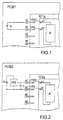
- Figure 1 shows schematically a printed circuit board, indicated PCB1, which contains an integrated-circuit device IC1g (the suffix 1g indicates that the integrated circuit device is of the "first generation") and a voltage supply V.
- the device IC1g has a plurality of terminal pins connected to corresponding connection areas of the board PCB1.
- the drawing shows only four pins connected to corresponding areas a1 - a4 of the board PCB1.
- Two of these pins, indicated VDD1 and VSS are connected to areas a1, a2 which are connected to the voltage supply V.
- the active portion of the integrated circuit is represented by a block A with terminals a1', a2' connected to the pins VDD1 and VSS.
- the board PCB1 contains various other components, not shown, which, together with the device IC1g, constitute the circuit system of an electronic device, for example, a cellular telephone.
- the voltage of the supply V is set at the design stage so as to be suitable for the characteristics of the device IC1g.
- the supply V is shown as a component mounted on the board PCB1 but, naturally, it could also be external to the board.
- Figure 2 shows how the circuit of the printed circuit board, indicated PCB2 in this case, has to be modified in order to use a second-generation integrated-circuit device IC2g produced by a reduction in scale of the dimensions of the first-generation device IC1g.
- the device IC2g is functionally equivalent to the device IC1g and has the same pin arrangement as the device IC1g, but its active portion A1' requires a lower supply voltage.
- the supply voltage V is reduced and stabilized by a regulator RG which has its output terminals connected to the supply terminals VDD2 and VSS of the device IC2g, and by a filter capacitor C connected in parallel with the output of the regulator.
- both the printed circuit board PCB and the first-generation integrated circuit IC1g' are designed taking account of possible future reductions in scale of the integrated circuit.
- the device IC1g' has an additional pin, indicated VDD2g, and an internal connection SC which short-circuits the pins VDD1g and VDD2g.
- the board PCB in turn has an additional connection area a+ to which the additional pin VDD2g is fixed and a capacitor C connected between the additional area a+ and the area a2 which is connected to the supply pin VSS.
- the additional pin VDD2g is entirely superfluous from the point of view of the operation of this circuit system and the capacitor C has the sole function of stabilizing the supply voltage.
- the capacitor C may be omitted if the stabilization function is not necessary and if there is no provision for integrated-circuit devices of generations subsequent to that of the device IC1g' to be mounted on the board PCB.
- Figure 4 shows the same board PCB as Figure 3, on which an integrated-circuit device IC2g' of a generation subsequent to that of the device IC1g' of Figure 3 and having an active portion A' is mounted.
- the integrated-circuit device again has an additional pin VDD2g and has the same pin arrangement as the device IC1g', but contains a voltage reducer/regulator RG instead of the short-circuit SC.
- the supply voltage V is reduced and stabilized at the value required for the supply of the active portion A' of the device IC2g'.
- the capacitor C which may have a value of between 1 and 10 ⁇ F, performs the function of filtering interference present at the supply terminals, for example, such as interference due to switching of the transistors of the logic gates in the circuit block A'.
- the higher supply voltage available at the terminal VDD1g can advantageously be used to supply any portions (not shown) of the integrated circuit which have not been reduced in scale, for example, because they are intended for digital input-output interface functions.
- the printed circuit board PCB does not have to be modified when the integrated circuit mounted thereon is replaced by an equivalent device of a subsequent technological generation, since the modifications necessary for the adaptation are made within the integrated circuit itself by the addition of a voltage regulator circuit.
- the area required by the regulator is generally very small and, in any case, smaller than the area saved by the reduction in scale. For example, by changing from 0.35 ⁇ m technology to 0.25 ⁇ m technology, an integrated circuit which originally occupied an area of 100 mm 2 can be produced in an area of 50 mm 2 , whereas the area required for a regulator is 2 - 3 mm 2 .
Landscapes
- Semiconductor Integrated Circuits (AREA)
Abstract

Description
- The present invention relates to the manufacture of circuit systems containing integrated-circuit devices and, more particularly, to a method of using, in a circuit system which is designed to operate with a first integrated-circuit device operating at a first supply voltage, a second integrated-circuit device having the same functional characteristics as the first device and comprising at least a portion operating at a second supply voltage. The invention also relates to a circuit system formed for implementing the method.
- It is known that, in the manufacture of integrated circuits, there is a tendency to reduce as far as possible the area of the substrate of semiconductor material, typically silicon, in which the integrated circuit is formed. The reduction in size is achieved by the use of more and more refined techniques and tooling which increase the precision of the photolithographic processes and improve control over diffusion.
- In the manufacture of MOS digital integrated circuits, the development of the technology is evident basically as a reduction in the minimum channel length which can be achieved for the transistors both of the logic circuits and of the memory cells, and as a reduction in the depth of the diffused source and drain regions of the transistors. These dimensional reductions are advantageous not only because of the saving in area involved, but also because of some functional aspects such as lower energy consumption and faster speed of operation.
- However, there are cases in which it is not possible to make use of these advantages. An example is a digital integrated circuit designed to perform a certain function as a component of a complex circuit system which is mounted, together with other components, on a printed circuit board. The supply voltage of the integrated circuit is set at the design stage at an optimal value which is determined by the minimum length of the channels of the transistors of the logic circuits. If the integrated circuit as a whole, or a portion thereof, is reproduced on a reduced scale with the use of more advanced manufacturing techniques, the optimal supply voltage is also reduced. For example, upon changing from 0.35 µm technology, which requires a supply voltage of 3.3 V ± 10%, to 0.25 µm technology, the supply voltage must be reduced to 2.5 V ± 10%. In order to use a new-generation integrated circuit in the circuit system which was designed for using the integrated circuit of the preceding generation, it is necessary to modify the printed circuit board, for example, by adding a voltage reducer thereto. This modification is necessary when the average life of the product which contains the circuit system is longer than that of the technology by which the integrated circuits used therein are produced. (Currently, the life of a technological generation is slightly less than one year.) It is therefore sometimes necessary to forego the advantages of technological progress and to keep obsolete production lines in operation to provide the supplies and the spare parts which are required by the manufacturers of the products, or to modify the circuit systems contained in these products in order to adapt them to equivalent new-generation integrated circuits. The first solution is disadvantageous for the manufacturer of the integrated-circuit devices and the second is disadvantageous for the manufacturer of the circuit systems; naturally, both of these solutions adversely affect the cost of the product.
- The object of the present invention is to define a method and to provide a circuit system for preventing the above-mentioned problems and thus to enable integrated-circuit devices of different generations to be used in the same circuit system without modifications or adaptations.
- This object is achieved by the implementation of the method defined in general in Claim 1 and by the provision of the circuit system defined in general in Claim 2.
- The invention will be understood better from the following detailed description of an embodiment thereof, given with reference to the appended drawings, in which:
- Figures 1 and 2 show schematically two circuit systems of the prior art comprising integrated circuits of two different generations, and
- Figures 3 and 4 show schematically two circuit systems according to the invention comprising integrated circuits of two different generations.
-
- Figure 1 shows schematically a printed circuit board, indicated PCB1, which contains an integrated-circuit device IC1g (the suffix 1g indicates that the integrated circuit device is of the "first generation") and a voltage supply V. The device IC1g has a plurality of terminal pins connected to corresponding connection areas of the board PCB1. The drawing shows only four pins connected to corresponding areas a1 - a4 of the board PCB1. Two of these pins, indicated VDD1 and VSS, are connected to areas a1, a2 which are connected to the voltage supply V. The active portion of the integrated circuit is represented by a block A with terminals a1', a2' connected to the pins VDD1 and VSS. The board PCB1 contains various other components, not shown, which, together with the device IC1g, constitute the circuit system of an electronic device, for example, a cellular telephone. The voltage of the supply V is set at the design stage so as to be suitable for the characteristics of the device IC1g. In this embodiment, the supply V is shown as a component mounted on the board PCB1 but, naturally, it could also be external to the board.
- Figure 2 shows how the circuit of the printed circuit board, indicated PCB2 in this case, has to be modified in order to use a second-generation integrated-circuit device IC2g produced by a reduction in scale of the dimensions of the first-generation device IC1g. The device IC2g is functionally equivalent to the device IC1g and has the same pin arrangement as the device IC1g, but its active portion A1' requires a lower supply voltage. For this purpose, the supply voltage V is reduced and stabilized by a regulator RG which has its output terminals connected to the supply terminals VDD2 and VSS of the device IC2g, and by a filter capacitor C connected in parallel with the output of the regulator.
- According to the invention, as shown in Figure 3, in which parts identical to those of Figure 1 are identified by the same reference symbols, both the printed circuit board PCB and the first-generation integrated circuit IC1g' are designed taking account of possible future reductions in scale of the integrated circuit. More particularly, the device IC1g' has an additional pin, indicated VDD2g, and an internal connection SC which short-circuits the pins VDD1g and VDD2g. The board PCB in turn has an additional connection area a+ to which the additional pin VDD2g is fixed and a capacitor C connected between the additional area a+ and the area a2 which is connected to the supply pin VSS. Naturally, the additional pin VDD2g is entirely superfluous from the point of view of the operation of this circuit system and the capacitor C has the sole function of stabilizing the supply voltage. Naturally, the capacitor C may be omitted if the stabilization function is not necessary and if there is no provision for integrated-circuit devices of generations subsequent to that of the device IC1g' to be mounted on the board PCB.
- Figure 4 shows the same board PCB as Figure 3, on which an integrated-circuit device IC2g' of a generation subsequent to that of the device IC1g' of Figure 3 and having an active portion A' is mounted. In this case, the integrated-circuit device again has an additional pin VDD2g and has the same pin arrangement as the device IC1g', but contains a voltage reducer/regulator RG instead of the short-circuit SC. The supply voltage V is reduced and stabilized at the value required for the supply of the active portion A' of the device IC2g'. In this case, the capacitor C, which may have a value of between 1 and 10 µF, performs the function of filtering interference present at the supply terminals, for example, such as interference due to switching of the transistors of the logic gates in the circuit block A'.
- It should be noted that the higher supply voltage available at the terminal VDD1g can advantageously be used to supply any portions (not shown) of the integrated circuit which have not been reduced in scale, for example, because they are intended for digital input-output interface functions.
- It is clear from the foregoing that, according to the invention, the printed circuit board PCB does not have to be modified when the integrated circuit mounted thereon is replaced by an equivalent device of a subsequent technological generation, since the modifications necessary for the adaptation are made within the integrated circuit itself by the addition of a voltage regulator circuit. It should be noted that the area required by the regulator is generally very small and, in any case, smaller than the area saved by the reduction in scale. For example, by changing from 0.35 µm technology to 0.25 µm technology, an integrated circuit which originally occupied an area of 100 mm2 can be produced in an area of 50 mm2, whereas the area required for a regulator is 2 - 3 mm2.
Claims (3)
- A method of using, in a circuit system (PCB) which is designed to operate with a first integrated-circuit device (IC1g') operating at a first supply voltage (V), a second integrated-circuit device (IC2g') functionally equivalent to the first integrated-circuit device (IC1g') and comprising at least a portion (A') operating at a second supply voltage lower than the first supply voltage,
characterized in that it comprises the following steps:providing, in the circuit system (PCB), a plurality of areas for connection to corresponding terminals of the first integrated-circuit device (IC1g') or of the second integrated-circuit device (IC2g'), two of these areas, which correspond to the supply terminals (VDD1g, VSS) of one or of the other of the integrated-circuit devices, being connected to the first voltage supply (V), and a third area, which corresponds to another terminal (VDD2g) of one or of the other of the integrated-circuited devices, being connected to circuit means (C) of the circuit system,forming, in the first integrated-circuit device (IC1g'), a direct electrical connection between the said other terminal (VDD2g) and one (VDD1g) of the terminals connected to the first voltage supply, andforming, in the second integrated-circuit device (IC2g'), a voltage-reducer circuit with regulator (RG) the output of which is connected to the said other terminal (VDD2g). - A circuit system comprising a voltage supply (V) and an integrated-circuit device (IC1g', IC2g') having a plurality of terminals of which two (VDD1g, VSS) are connected to the voltage supply (V),
characterized in that the integrated-circuit device is one of a family of functionally equivalent devices that comprises a first-generation integrated-circuit device (IC1g') operating at the supply voltage and at least one subsequent-generation integrated-circuit device (IC2g') at least a portion (A') of which operates at a voltage lower than the supply voltage (V), the first-generation device (IC1g') comprising a direct electrical connection (SC) between one (VDD1g) of the terminals connected to the supply and another terminal (VDD2g) of the plurality of terminals, and the subsequent-generation device (IC2g') comprising a voltage-reducer circuit with regulator (RG) the output of which is connected to the said other terminal (VDD2g). - A circuit system according to Claim 2, comprising capacitive means (C) external to the integrated-circuit device (IC2g') and connected between the said other terminal (VDD2g) and one (VSS) of the terminals connected to the supply (V).
Priority Applications (3)
| Application Number | Priority Date | Filing Date | Title |
|---|---|---|---|
| DE60037242T DE60037242D1 (en) | 2000-05-04 | 2000-05-04 | A method and circuit systems for using equivalent integrated circuit elements with different operating voltages |
| EP00830323A EP1152465B1 (en) | 2000-05-04 | 2000-05-04 | A method and a circuit system for using equivalent integrated-circuit devices operating at different voltages |
| US09/848,615 US6768649B2 (en) | 2000-05-04 | 2001-05-03 | Method and a circuit system for using equivalent integrated-circuit devices operating at different voltages |
Applications Claiming Priority (1)
| Application Number | Priority Date | Filing Date | Title |
|---|---|---|---|
| EP00830323A EP1152465B1 (en) | 2000-05-04 | 2000-05-04 | A method and a circuit system for using equivalent integrated-circuit devices operating at different voltages |
Publications (2)
| Publication Number | Publication Date |
|---|---|
| EP1152465A1 true EP1152465A1 (en) | 2001-11-07 |
| EP1152465B1 EP1152465B1 (en) | 2007-11-28 |
Family
ID=8175311
Family Applications (1)
| Application Number | Title | Priority Date | Filing Date |
|---|---|---|---|
| EP00830323A Expired - Lifetime EP1152465B1 (en) | 2000-05-04 | 2000-05-04 | A method and a circuit system for using equivalent integrated-circuit devices operating at different voltages |
Country Status (3)
| Country | Link |
|---|---|
| US (1) | US6768649B2 (en) |
| EP (1) | EP1152465B1 (en) |
| DE (1) | DE60037242D1 (en) |
Families Citing this family (3)
| Publication number | Priority date | Publication date | Assignee | Title |
|---|---|---|---|---|
| US7765418B2 (en) * | 2007-03-15 | 2010-07-27 | Qimonda North America Corp. | Multi-mode voltage supply circuit |
| JP5657264B2 (en) * | 2010-03-31 | 2015-01-21 | ラピスセミコンダクタ株式会社 | Semiconductor integrated circuit device |
| DE102018220149B3 (en) * | 2018-11-23 | 2020-03-12 | Phoenix Contact Gmbh & Co. Kg | Assembly with an electrotechnical component on a carrier |
Citations (3)
| Publication number | Priority date | Publication date | Assignee | Title |
|---|---|---|---|---|
| US5132555A (en) * | 1990-02-23 | 1992-07-21 | Hitachi, Ltd. | Semiconductor integrated circuit |
| US5444298A (en) * | 1993-02-04 | 1995-08-22 | Intel Corporation | Voltage converting integrated circuit package |
| US5556811A (en) * | 1993-12-21 | 1996-09-17 | Intel Corporation | Method of optimizing operating parameters of an integrated circuit package having a voltage regulator mounted thereon |
Family Cites Families (4)
| Publication number | Priority date | Publication date | Assignee | Title |
|---|---|---|---|---|
| US5627460A (en) * | 1994-12-28 | 1997-05-06 | Unitrode Corporation | DC/DC converter having a bootstrapped high side driver |
| US5694297A (en) * | 1995-09-05 | 1997-12-02 | Astec International Limited | Integrated circuit mounting structure including a switching power supply |
| JP2001110184A (en) * | 1999-10-14 | 2001-04-20 | Hitachi Ltd | Semiconductor device |
| US6504735B2 (en) * | 2001-03-12 | 2003-01-07 | 02 Micro International Ltd. | Regulated voltage reducing high-voltage isolated DC/DC converter system |
-
2000
- 2000-05-04 DE DE60037242T patent/DE60037242D1/en not_active Expired - Lifetime
- 2000-05-04 EP EP00830323A patent/EP1152465B1/en not_active Expired - Lifetime
-
2001
- 2001-05-03 US US09/848,615 patent/US6768649B2/en not_active Expired - Lifetime
Patent Citations (3)
| Publication number | Priority date | Publication date | Assignee | Title |
|---|---|---|---|---|
| US5132555A (en) * | 1990-02-23 | 1992-07-21 | Hitachi, Ltd. | Semiconductor integrated circuit |
| US5444298A (en) * | 1993-02-04 | 1995-08-22 | Intel Corporation | Voltage converting integrated circuit package |
| US5556811A (en) * | 1993-12-21 | 1996-09-17 | Intel Corporation | Method of optimizing operating parameters of an integrated circuit package having a voltage regulator mounted thereon |
Also Published As
| Publication number | Publication date |
|---|---|
| EP1152465B1 (en) | 2007-11-28 |
| DE60037242D1 (en) | 2008-01-10 |
| US6768649B2 (en) | 2004-07-27 |
| US20020022402A1 (en) | 2002-02-21 |
Similar Documents
| Publication | Publication Date | Title |
|---|---|---|
| US10748933B2 (en) | Semiconductor device | |
| US7443224B2 (en) | Multi-threshold MIS integrated circuit device and circuit design method thereof | |
| US20050235240A1 (en) | Method for reducing layers revision in engineering change order | |
| JP2888898B2 (en) | Semiconductor integrated circuit | |
| US5763907A (en) | Library of standard cells for the design of integrated circuits | |
| JP2007184650A (en) | Mount for programmable electronic processing equipment | |
| US7882476B2 (en) | Semiconductor integrated circuit device formed by automatic layout wiring by use of standard cells and design method of fixing its well potential | |
| EP1152465B1 (en) | A method and a circuit system for using equivalent integrated-circuit devices operating at different voltages | |
| US8384163B2 (en) | Layout design tool for semiconductor integrated circuit | |
| US6271704B1 (en) | Method and apparatus for balancing current in a system with two sets of termination devices | |
| JP2002076285A (en) | Electric device and LSI incorporating a plurality of LSIs | |
| JP4562456B2 (en) | Semiconductor integrated circuit | |
| US20080296628A1 (en) | Semiconductor integrated circuit and method for manufacturing same | |
| KR200169860Y1 (en) | Structure of voltage regulator | |
| US6870250B2 (en) | Chip package structure having π filter | |
| US20030208738A1 (en) | Design method for full chip element on memory | |
| US20020030513A1 (en) | Logic circuit cell constituting an integrated circuit and cell library having a collection of logic circuit cells | |
| EP1009031A2 (en) | Semiconductor integrated circuit device and method of producing the same | |
| US6924666B2 (en) | Integrated logic circuit and hierarchical design method thereof | |
| US6946875B2 (en) | Universal logic module and ASIC using the same | |
| JPH01208840A (en) | Semiconductor integrated circuit device | |
| KR19980065642A (en) | Output pad arrangement method of semiconductor memory device | |
| US20020167802A1 (en) | Printed circuit board | |
| JPH04127377A (en) | Designing method for printed circuit board | |
| US20090153187A1 (en) | Monolithically integrated interface circuit |
Legal Events
| Date | Code | Title | Description |
|---|---|---|---|
| PUAI | Public reference made under article 153(3) epc to a published international application that has entered the european phase |
Free format text: ORIGINAL CODE: 0009012 |
|
| AK | Designated contracting states |
Kind code of ref document: A1 Designated state(s): AT BE CH CY DE DK ES FI FR GB GR IE IT LI LU MC NL PT SE |
|
| AX | Request for extension of the european patent |
Free format text: AL;LT;LV;MK;RO;SI |
|
| 17P | Request for examination filed |
Effective date: 20020318 |
|
| AKX | Designation fees paid |
Free format text: DE FR GB IT |
|
| 17Q | First examination report despatched |
Effective date: 20050202 |
|
| GRAP | Despatch of communication of intention to grant a patent |
Free format text: ORIGINAL CODE: EPIDOSNIGR1 |
|
| GRAS | Grant fee paid |
Free format text: ORIGINAL CODE: EPIDOSNIGR3 |
|
| GRAA | (expected) grant |
Free format text: ORIGINAL CODE: 0009210 |
|
| AK | Designated contracting states |
Kind code of ref document: B1 Designated state(s): DE FR GB IT |
|
| REG | Reference to a national code |
Ref country code: GB Ref legal event code: FG4D |
|
| REF | Corresponds to: |
Ref document number: 60037242 Country of ref document: DE Date of ref document: 20080110 Kind code of ref document: P |
|
| EN | Fr: translation not filed | ||
| PGFP | Annual fee paid to national office [announced via postgrant information from national office to epo] |
Ref country code: IT Payment date: 20080520 Year of fee payment: 9 |
|
| PLBE | No opposition filed within time limit |
Free format text: ORIGINAL CODE: 0009261 |
|
| STAA | Information on the status of an ep patent application or granted ep patent |
Free format text: STATUS: NO OPPOSITION FILED WITHIN TIME LIMIT |
|
| PG25 | Lapsed in a contracting state [announced via postgrant information from national office to epo] |
Ref country code: FR Free format text: LAPSE BECAUSE OF FAILURE TO SUBMIT A TRANSLATION OF THE DESCRIPTION OR TO PAY THE FEE WITHIN THE PRESCRIBED TIME-LIMIT Effective date: 20080912 Ref country code: DE Free format text: LAPSE BECAUSE OF FAILURE TO SUBMIT A TRANSLATION OF THE DESCRIPTION OR TO PAY THE FEE WITHIN THE PRESCRIBED TIME-LIMIT Effective date: 20080229 |
|
| 26N | No opposition filed |
Effective date: 20080829 |
|
| GBPC | Gb: european patent ceased through non-payment of renewal fee |
Effective date: 20080504 |
|
| PG25 | Lapsed in a contracting state [announced via postgrant information from national office to epo] |
Ref country code: GB Free format text: LAPSE BECAUSE OF NON-PAYMENT OF DUE FEES Effective date: 20080504 |
|
| PG25 | Lapsed in a contracting state [announced via postgrant information from national office to epo] |
Ref country code: IT Free format text: LAPSE BECAUSE OF NON-PAYMENT OF DUE FEES Effective date: 20090504 |