EP1150448A2 - Demultiplexer control system - Google Patents
Demultiplexer control system Download PDFInfo
- Publication number
- EP1150448A2 EP1150448A2 EP01201461A EP01201461A EP1150448A2 EP 1150448 A2 EP1150448 A2 EP 1150448A2 EP 01201461 A EP01201461 A EP 01201461A EP 01201461 A EP01201461 A EP 01201461A EP 1150448 A2 EP1150448 A2 EP 1150448A2
- Authority
- EP
- European Patent Office
- Prior art keywords
- timing
- control signal
- modulator
- decompressed
- pulse train
- Prior art date
- Legal status (The legal status is an assumption and is not a legal conclusion. Google has not performed a legal analysis and makes no representation as to the accuracy of the status listed.)
- Granted
Links
- 230000003287 optical effect Effects 0.000 claims abstract description 23
- 238000000034 method Methods 0.000 claims abstract description 12
- 230000000694 effects Effects 0.000 claims abstract description 10
- 238000012544 monitoring process Methods 0.000 claims abstract description 8
- 230000003111 delayed effect Effects 0.000 claims description 2
- 239000000284 extract Substances 0.000 claims description 2
- 238000004891 communication Methods 0.000 abstract description 2
- 230000001934 delay Effects 0.000 abstract description 2
- 230000005540 biological transmission Effects 0.000 description 2
- 238000007906 compression Methods 0.000 description 2
- 230000006835 compression Effects 0.000 description 2
- 238000013144 data compression Methods 0.000 description 2
- 238000010586 diagram Methods 0.000 description 2
- 238000005259 measurement Methods 0.000 description 2
- 230000032683 aging Effects 0.000 description 1
- 238000013459 approach Methods 0.000 description 1
- 230000007423 decrease Effects 0.000 description 1
- 238000011161 development Methods 0.000 description 1
- 230000018109 developmental process Effects 0.000 description 1
- 239000013307 optical fiber Substances 0.000 description 1
Images


Classifications
-
- H—ELECTRICITY
- H04—ELECTRIC COMMUNICATION TECHNIQUE
- H04J—MULTIPLEX COMMUNICATION
- H04J14/00—Optical multiplex systems
- H04J14/08—Time-division multiplex systems
-
- H—ELECTRICITY
- H04—ELECTRIC COMMUNICATION TECHNIQUE
- H04B—TRANSMISSION
- H04B10/00—Transmission systems employing electromagnetic waves other than radio-waves, e.g. infrared, visible or ultraviolet light, or employing corpuscular radiation, e.g. quantum communication
Definitions
- the present invention relates to a demultiplexer control system.
- the present invention relates to a control system to enable the control of the demultiplexing process associated with an optical backplane.
- the invention has application in the development of new architectures for optical switching applied to high-speed digital communication routers/switches.
- UK Patent Application No. 9930163.2 - “Data Compression Apparatus and Method Therefor” describes the operation of an optical backplane, for example an optical fibre, in an optical switching system.
- the operation includes a method for converting packets of data at 10 Gbits/s to packets at 1.28 Tbits/s.
- the compressed packets are time multiplexed onto the optical backplane of a switching device, for example an IP router or ATM switch.
- the process of selecting a given compressed packet, from the stream of multiplexed packets on the backplane, is termed demultiplexing the packet.
- a laser generates (step 400) a pulse having a duration corresponding to the length of an input packet of data and a linear chirp, i.e. the frequency of the light increases (or decreases) with time during the pulse.
- Packets of data corresponding to the input data are received (step 402) by input receiver transducers.
- the data received is buffered (step 404).
- the buffered data is then transferred to a modulator controller for modulation (step 406) by a modulator.
- a modulated data signal from the modulator is then compressed (step 408) by a compressor.
- a delay is introduced (step 410) to facilitate multiplexing of compressed data pulses.
- Modulated data signals are combined (step 412) and form a multiplexed compressed modulated pulse train.
- the combined multiplexed pulse train is carried by an optical backplane then split and sent to at least one modulator where it is demultiplexed (step 414).
- the demultiplexed, compressed packet is decompressed once it has passed through the modulator (step 416).
- the resulting decompressed packet is converted from an optical signal to an electrical signal.
- the decompressed, demultiplexed packet is received by output receiver transducers (step 418).
- the output receiver transducers convert the optical signals received to 10 Gbits/s electrical signals.
- the signals generated by the output receiver transducers are buffered (step 420) before they are forwarded to output transmitter transducers.
- the output transmitter transducers convert the received electrical signal to a 10 Gbits/s optical signal for further transmission (step 422).
- Demultiplexing (step 414) is carried out by supplying the multiplexed pulse train of compressed packets to a modulator that is normally in an 'off' state.
- the modulator attenuates, deflects or otherwise blocks the packets whilst in the 'off' state.
- the modulator is arranged to be switched to an 'on' state when the required compressed packet arrives, thus allowing the selected compressed packet to pass through the modulator.
- the modulator In the systems of relevance to IP routers, the modulator is typically in an 'on' state for 50 picoseconds (ps). If the time when the modulator is turned 'on' does not match the arrival of a compressed packet, part of the compressed packet will be lost and the detected signal will be in error. The timing error has only to be of the order of ten picoseconds to degrade the performance of the switch. Timing errors of this order are common in electrical and optical systems as a result of temperature and other physical changes. In order to ensure that the switch continues to operate effectively, the relative timing of the modulator control signal and the compressed packet must be monitored and periodically adjusted to keep them in their correct relationship.
- the compressed data packet signal needs to be measured with a very high bandwidth (many tens of gigaHertz (GHz)), which is costly, high in power consumption (therefore heat generating) and difficult to implement.
- GHz gigaHertz
- a system for controlling the demultiplexing process in an optical backplane device including: a modulator means, which is controlled by a modulator control signal and which extracts a selected compressed data packet from a multiplexed stream of compressed packets; a monitoring means, wherein the effect of timing errors on decompressed signals is monitored; and a control signal adjusting means, wherein the timing errors are corrected by adjusting the timing of the modulator control signal.
- the timing of modulator control signal is continuously adjusted to minimise timing errors.
- the timing of the modulator control signal is preferably advanced if the trailing edge of a given decompressed pulse train is reduced more than the leading edge of said decompressed pulse train and delayed if the leading edge of the given decompressed pulse train is reduced more than the trailing edge of said decompressed pulse train.
- both the delay and the advance are proportional to the difference in reduction between the leading and trailing edges.
- the timing of the modulator control signal makes use of calibration pulse trains of known value and suitable form to adjust the timing of modulator control pulses.
- the timing of the modulator control signal may make use of a calibration pulse train consisting of binary 'ones' only.
- the timing of the modulator control signal may make use of a calibration pulse train consisting of a finite repeating sequence of binary 'one' followed by binary 'zero'.
- Figure 1 shows how demultiplexing is carried out by supplying the stream of multiplexed compressed packets 110 to a modulator 102 that is normally in an 'off' state.
- the modulator 102 attenuates, deflects or otherwise blocks the packets 110 whilst in the 'off' state.
- the modulator 102 is arranged to be switched to an 'on' state when the required compressed packet 120 arrives, thus allowing the selected compressed packet 120 to pass through the modulator 102.
- the selected compressed packet 120 is decompressed 104 after passing through the modulator 102.
- the resulting decompressed packet 116 is converted from an optical signal to an electrical signal by a converter 106: in other words the decompressed packet 116 is 'detected'.
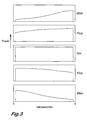
- Figure 2 shows the effect on the decompressed signal of the timing error at timing errors of -20 ps, -10 ps, zero error, +10ps and +20 ps. It can be seen that if the timing error is negative the leading edge of the decompressed pulse train is reduced more than the other end, whereas if the timing error is positive the trailing edge is reduced more.
- the timing error effect gives an unambiguous indication of the direction and amount of the timing error and by controlling delays in either the optical or electronic parts of the system, the error can then be corrected for.
- the distortion can be continuously monitored and the timing adjusted continuously to minimise the timing drifts due to phenomena including temperature, ageing and mechanical effects.
- One method for arranging a suitable distortion is to make the compressor an imperfect match to the laser chirp.
- the signal is not compressed to its full extent.
- the signal being compressed to a lesser extent is, in any case, desirable to reduce the peak power in the compressed signal. It should be remarked that a small degree of incomplete compression has little effect on the performance of the system.
- the distortion can be monitored by looking at the signal level of the data pulses along the length of the decompressed pulse. If the data is non-return to zero (NRZ) this process would have to be averaged over a number of decompressed pulse trains, since in any given pulse train there may be no pulses to measure, at either one or both end portions of the pulse train.
- NTZ non-return to zero
- calibration pulse trains that consist of a known and suitable set of pulses. Use of calibration pulse trains has a cost because it reduces the transmission bandwidth available to other functions of the system. However, if the uncorrected timing error changes very much more slowly than the data rate then this loss of capacity will not be significant.
- a calibration pulse train of alternating 'ones' and 'zeros' can be adopted. Again the distortion introduced by timing errors can be monitored in a simple manner.
- the monitoring of distortion need not involve making measurements of the pulse height at the full data bandwidth.
- the measurement system is therefore made much easier and less costly.
Abstract
Description
- The present invention relates to a demultiplexer control system. In particular, the present invention relates to a control system to enable the control of the demultiplexing process associated with an optical backplane.
- The invention has application in the development of new architectures for optical switching applied to high-speed digital communication routers/switches.
- UK Patent Application No. 9930163.2 - "Data Compression Apparatus and Method Therefor" describes the operation of an optical backplane, for example an optical fibre, in an optical switching system. The operation includes a method for converting packets of data at 10 Gbits/s to packets at 1.28 Tbits/s. In the next step after data compression, the compressed packets are time multiplexed onto the optical backplane of a switching device, for example an IP router or ATM switch. The process of selecting a given compressed packet, from the stream of multiplexed packets on the backplane, is termed demultiplexing the packet.
- The operation of an optical switching device wherein pulse trains are time multiplexed on an optical backplane is shown in Figure 4. A laser generates (step 400) a pulse having a duration corresponding to the length of an input packet of data and a linear chirp, i.e. the frequency of the light increases (or decreases) with time during the pulse. Packets of data corresponding to the input data are received (step 402) by input receiver transducers. The data received is buffered (step 404). The buffered data is then transferred to a modulator controller for modulation (step 406) by a modulator.
- A modulated data signal from the modulator is then compressed (step 408) by a compressor. In the case of compressed data pulses corresponding to subsequent input data, a delay is introduced (step 410) to facilitate multiplexing of compressed data pulses. Modulated data signals are combined (step 412) and form a multiplexed compressed modulated pulse train. The combined multiplexed pulse train is carried by an optical backplane then split and sent to at least one modulator where it is demultiplexed (step 414).
- The demultiplexed, compressed packet is decompressed once it has passed through the modulator (step 416). The resulting decompressed packet is converted from an optical signal to an electrical signal.
- The decompressed, demultiplexed packet is received by output receiver transducers (step 418). The output receiver transducers convert the optical signals received to 10 Gbits/s electrical signals. The signals generated by the output receiver transducers are buffered (step 420) before they are forwarded to output transmitter transducers. Finally, the output transmitter transducers convert the received electrical signal to a 10 Gbits/s optical signal for further transmission (step 422).
- Demultiplexing (step 414) is carried out by supplying the multiplexed pulse train of compressed packets to a modulator that is normally in an 'off' state. The modulator attenuates, deflects or otherwise blocks the packets whilst in the 'off' state. The modulator is arranged to be switched to an 'on' state when the required compressed packet arrives, thus allowing the selected compressed packet to pass through the modulator.
- In the systems of relevance to IP routers, the modulator is typically in an 'on' state for 50 picoseconds (ps). If the time when the modulator is turned 'on' does not match the arrival of a compressed packet, part of the compressed packet will be lost and the detected signal will be in error. The timing error has only to be of the order of ten picoseconds to degrade the performance of the switch. Timing errors of this order are common in electrical and optical systems as a result of temperature and other physical changes. In order to ensure that the switch continues to operate effectively, the relative timing of the modulator control signal and the compressed packet must be monitored and periodically adjusted to keep them in their correct relationship.
- One approach to achieving this monitoring would be to measure the control pulse and the peak of the compressed data packet and to compare them. This has a number of disadvantages. Firstly, the compressed data packet signal needs to be measured with a very high bandwidth (many tens of gigaHertz (GHz)), which is costly, high in power consumption (therefore heat generating) and difficult to implement.
- Secondly, errors on the comparison process are as difficult to avoid as errors in the modulator timing.
- Thus there is a need for a technique which enables the timing to be monitored and adjusted without having to measure the signals with picosecond accuracy or bandwidths of many tens of gigaHertz.
- It is therefore an object of the invention to obviate or at least mitigate the aforementioned problems.
- In accordance with one aspect of the present invention, there is provided a system for controlling the demultiplexing process in an optical backplane device, the optical backplane device including: a modulator means, which is controlled by a modulator control signal and which extracts a selected compressed data packet from a multiplexed stream of compressed packets; a monitoring means, wherein the effect of timing errors on decompressed signals is monitored; and a control signal adjusting means, wherein the timing errors are corrected by adjusting the timing of the modulator control signal.
- Preferably, the timing of modulator control signal is continuously adjusted to minimise timing errors.
- The timing of the modulator control signal is preferably advanced if the trailing edge of a given decompressed pulse train is reduced more than the leading edge of said decompressed pulse train and delayed if the leading edge of the given decompressed pulse train is reduced more than the trailing edge of said decompressed pulse train.
- Advantageously, both the delay and the advance are proportional to the difference in reduction between the leading and trailing edges.
- Preferably, the timing of the modulator control signal makes use of calibration pulse trains of known value and suitable form to adjust the timing of modulator control pulses.
- The timing of the modulator control signal may make use of a calibration pulse train consisting of binary 'ones' only. Alternatively, the timing of the modulator control signal may make use of a calibration pulse train consisting of a finite repeating sequence of binary 'one' followed by binary 'zero'.
- For a better understanding of the present invention, reference will now be made, by way of example only, to the accompanying drawings in which:
- Figure 1 shows a schematic diagram of the demultiplexing process;
- Figure 2 illustrates the distorting effect of demultiplexer timing error on a decompressed signal;
- Figure 3 illustrates the distorting effect of demultiplexer timing error on a calibration pulse train of all 'ones' as may be used in the present invention; and
- Figure 4 shows a schematic diagram of the operation of an optical switching devices using time multiplexing of pulse trains on an optical backplane as disclosed in UK Patent Application No. 9930163.2.
-
- Figure 1 shows how demultiplexing is carried out by supplying the stream of multiplexed
compressed packets 110 to amodulator 102 that is normally in an 'off' state. Themodulator 102 attenuates, deflects or otherwise blocks thepackets 110 whilst in the 'off' state. Themodulator 102 is arranged to be switched to an 'on' state when the requiredcompressed packet 120 arrives, thus allowing the selectedcompressed packet 120 to pass through themodulator 102. The selectedcompressed packet 120 is decompressed 104 after passing through themodulator 102. The resultingdecompressed packet 116 is converted from an optical signal to an electrical signal by a converter 106: in other words thedecompressed packet 116 is 'detected'. - When a signal is less than completely compressed, an error in the timing of the modulator control signal can be arranged so that the decompressed signal is distorted in a specific way. The effect of timing errors in the demultiplexer control signal when incomplete compression is implemented, is illustrated in Figure 2.
- Figure 2 shows the effect on the decompressed signal of the timing error at timing errors of -20 ps, -10 ps, zero error, +10ps and +20 ps. It can be seen that if the timing error is negative the leading edge of the decompressed pulse train is reduced more than the other end, whereas if the timing error is positive the trailing edge is reduced more.
- The timing error effect gives an unambiguous indication of the direction and amount of the timing error and by controlling delays in either the optical or electronic parts of the system, the error can then be corrected for. Thus the distortion can be continuously monitored and the timing adjusted continuously to minimise the timing drifts due to phenomena including temperature, ageing and mechanical effects.
- One method for arranging a suitable distortion is to make the compressor an imperfect match to the laser chirp. Crucially, therefore, the signal is not compressed to its full extent. The signal being compressed to a lesser extent is, in any case, desirable to reduce the peak power in the compressed signal. It should be remarked that a small degree of incomplete compression has little effect on the performance of the system.
- The distortion can be monitored by looking at the signal level of the data pulses along the length of the decompressed pulse. If the data is non-return to zero (NRZ) this process would have to be averaged over a number of decompressed pulse trains, since in any given pulse train there may be no pulses to measure, at either one or both end portions of the pulse train. Thus it is advantageous to use specially inserted, calibration pulse trains that consist of a known and suitable set of pulses. Use of calibration pulse trains has a cost because it reduces the transmission bandwidth available to other functions of the system. However, if the uncorrected timing error changes very much more slowly than the data rate then this loss of capacity will not be significant.
- The use of a calibration pulse train is illustrated in Figure 3. In this case, the calibration pulse is all 'ones' and it can be seen that monitoring of the distortion is straightforward.
- Similarly, a calibration pulse train of alternating 'ones' and 'zeros' can be adopted. Again the distortion introduced by timing errors can be monitored in a simple manner.
- If a calibration pulse train is not used, then the data in the pulse train will need to be taken into account when assessing the distortion. This can be done but involves considerably a monitoring means of considerably more complexity.
- It will be understood that the monitoring of distortion need not involve making measurements of the pulse height at the full data bandwidth. The measurement system is therefore made much easier and less costly.
Claims (8)
- A system for controlling the demultiplexing process in an optical backplane device, the optical backplane device including:a modulator means, which is controlled by a modulator control signal and which extracts a selected compressed data packet from a multiplexed stream of compressed packets;a monitoring means, wherein the effect of timing errors on decompressed pulse trains is monitored, each decompressed pulse train having a leading edge and a trailing edge; anda control signal adjusting means, wherein the timing errors are corrected by adjusting the timing of the modulator control signal.
- A system as claimed in Claim 1, wherein the timing of the modulator control signal is continuously adjusted to minimise timing errors.
- A system as claimed in Claims 1 or 2, wherein the timing of the modulator control signal is advanced if the trailing edge of a given decompressed pulse train is reduced more than the leading edge of said decompressed pulse train and delayed if the leading edge of the given decompressed pulse train is reduced more than the trailing edge of said decompressed pulse train.
- A system as claimed in Claim 3, wherein both the delay and the advance are proportional to the difference in reduction between the leading and trailing edges.
- A system as claimed in any one of Claims 1 to 4, wherein the timing of the modulator control signal makes use of calibration pulse trains of known value and suitable form to adjust the timing of modulator control pulses.
- A system as claimed in Claim 5, wherein the timing of the modulator control signal makes use of a calibration pulse train consisting of binary 'ones' only.
- A system as claimed in Claim 5, wherein the timing of the modulator control signal makes use of a calibration pulse train consisting of a finite repeating sequence of binary 'one' followed by binary 'zero'.
- A system substantially as hereinbefore described with reference to the accompanying Figures 1, 2 and 3.
Applications Claiming Priority (2)
| Application Number | Priority Date | Filing Date | Title |
|---|---|---|---|
| GB0010316 | 2000-04-28 | ||
| GB0010316A GB2361847B (en) | 2000-04-28 | 2000-04-28 | Demultiplexer control system and method |
Publications (3)
| Publication Number | Publication Date |
|---|---|
| EP1150448A2 true EP1150448A2 (en) | 2001-10-31 |
| EP1150448A3 EP1150448A3 (en) | 2006-06-07 |
| EP1150448B1 EP1150448B1 (en) | 2011-01-26 |
Family
ID=9890644
Family Applications (1)
| Application Number | Title | Priority Date | Filing Date |
|---|---|---|---|
| EP01201461A Expired - Lifetime EP1150448B1 (en) | 2000-04-28 | 2001-04-23 | Demultiplexer control system |
Country Status (8)
| Country | Link |
|---|---|
| US (1) | US7006766B2 (en) |
| EP (1) | EP1150448B1 (en) |
| JP (1) | JP2002033717A (en) |
| AT (1) | ATE497286T1 (en) |
| CA (1) | CA2345404C (en) |
| DE (1) | DE60143924D1 (en) |
| ES (1) | ES2361729T3 (en) |
| GB (1) | GB2361847B (en) |
Family Cites Families (9)
| Publication number | Priority date | Publication date | Assignee | Title |
|---|---|---|---|---|
| JP2719397B2 (en) * | 1989-04-24 | 1998-02-25 | 日本電信電話株式会社 | Ultrashort optical pulse modulation circuit |
| US5121240A (en) * | 1990-08-29 | 1992-06-09 | The Trustees Of Columbia University In The City Of New York | Optical packet time compression and expansion |
| IT1257546B (en) * | 1992-06-15 | 1996-01-30 | Cselt Centro Studi Lab Telecom | OPTICAL SWITCH FOR FAST CELL SWITCHING NETWORKS. |
| JP3156742B2 (en) * | 1993-11-04 | 2001-04-16 | 日本電信電話株式会社 | Optical demultiplexer |
| CA2190859C (en) * | 1994-05-23 | 2002-01-15 | David Cotter | Optical telecommunications network |
| JPH10178418A (en) * | 1996-12-19 | 1998-06-30 | Fujitsu Ltd | Optical time division demultiplexer, demultiplex signal changeover method and optical time division multiplex system |
| FR2765055B1 (en) * | 1997-06-23 | 1999-09-24 | Alsthom Cge Alcatel | METHOD AND DEVICE FOR CONCATENING BINARY INFORMATION AND APPLICATION TO OPTICAL PACKET TRANSMISSION |
| US6204944B1 (en) * | 1997-07-18 | 2001-03-20 | Nippon Telegraph And Telephone Corporation | All-optical time-division demultiplexing circuit and all-optical TDM-WDM conversion circuit |
| JP2002503916A (en) * | 1998-02-17 | 2002-02-05 | ザ、リージェンツ、オブ、ザ、ユニバーシティ、オブ、ミシガン | Self-synchronization method and system for optical packet network |
-
2000
- 2000-04-28 GB GB0010316A patent/GB2361847B/en not_active Expired - Lifetime
-
2001
- 2001-04-23 ES ES01201461T patent/ES2361729T3/en not_active Expired - Lifetime
- 2001-04-23 AT AT01201461T patent/ATE497286T1/en not_active IP Right Cessation
- 2001-04-23 DE DE60143924T patent/DE60143924D1/en not_active Expired - Lifetime
- 2001-04-23 EP EP01201461A patent/EP1150448B1/en not_active Expired - Lifetime
- 2001-04-26 US US09/842,207 patent/US7006766B2/en not_active Expired - Fee Related
- 2001-04-27 JP JP2001130678A patent/JP2002033717A/en active Pending
- 2001-04-27 CA CA2345404A patent/CA2345404C/en not_active Expired - Fee Related
Non-Patent Citations (3)
| Title |
|---|
| BOLOW H: "ELECTRONICS LETTERS", IEE STEVENAGE, vol. 31, no. 22, 26 October 1995 (1995-10-26), pages 1937 - 1938 |
| GAMBINI P ET AL.: "IEEE JOURNAL ON SELECTED AREAS IN COMMUNICATIONS", IEEE SERVICE CENTER, PISCATAWAY, NJ, US, vol. 16, no. 7, September 1998 (1998-09-01), pages 1245 - 1 259 |
| JINNO M ET AL.: "PROCEEDINGS OF THE OPTICAL FIBER COMMUNICATION CONFERENCE", IEEE, US, VOL. CONF., vol. 14, 18 February 1991 (1991-02-18), pages 49 |
Also Published As
| Publication number | Publication date |
|---|---|
| ES2361729T3 (en) | 2011-06-21 |
| CA2345404A1 (en) | 2001-10-28 |
| US7006766B2 (en) | 2006-02-28 |
| JP2002033717A (en) | 2002-01-31 |
| EP1150448A3 (en) | 2006-06-07 |
| GB2361847A (en) | 2001-10-31 |
| DE60143924D1 (en) | 2011-03-10 |
| GB2361847B (en) | 2003-12-03 |
| ATE497286T1 (en) | 2011-02-15 |
| US20020008890A1 (en) | 2002-01-24 |
| GB0010316D0 (en) | 2000-06-14 |
| EP1150448B1 (en) | 2011-01-26 |
| CA2345404C (en) | 2011-03-22 |
Similar Documents
| Publication | Publication Date | Title |
|---|---|---|
| EP1949569B1 (en) | Polarization compensation in a coherent optical receiver | |
| EP1379042B1 (en) | Multiplexer | |
| US20100232798A1 (en) | Bit identification circuit | |
| JP2007243796A (en) | Multi-rate pon system and terminal device used therefor | |
| US6619867B1 (en) | Optical transmission system | |
| CA2345404C (en) | Demultiplexer control system | |
| JP2627615B2 (en) | ATM cell precision synchronization method and device in optical ATM node | |
| Habara et al. | Demonstration of frequency-routing type photonic ATM switch (FRONTIERNET) prototype | |
| US7623795B1 (en) | Data compression apparatus and method therefor | |
| US7187869B2 (en) | Method for adjusting time delays and device for synchronization of channels in a WDM system | |
| EP1249087B1 (en) | Improved data compression apparatus and method therefor | |
| CA2434768C (en) | Optical data compression device and method | |
| US20020001114A1 (en) | Method and apparatus for demultiplexing high bit rate optical signals on dense wavelength grid | |
| EP3349374A1 (en) | Method for compensating crosstalk in an optical communication system | |
| AU2002235944A1 (en) | Optical data compression device and method | |
| JP2004274547A (en) | Optical signal processing device | |
| WO2024038543A1 (en) | Optically modulated signal generation device and transmission module | |
| Rangarajan et al. | Scalable all-optical compression/decompression of variable length (40 to 1500 byte) packets | |
| Clausen et al. | Pilot tone modulation used for channel identification in OTDM networks | |
| Gomez-Agis et al. | 160-Gbit/s packet clock distribution with instantaneous synchronization and low timing jitter | |
| JPH11145938A (en) | Photoelectric synchronizing device | |
| GB2376142A (en) | Multiplexing compressed optical data pulses | |
| JPH0758777A (en) | Optical synchronizing circuit and high speed optical packet detecting circuit using the same |
Legal Events
| Date | Code | Title | Description |
|---|---|---|---|
| PUAI | Public reference made under article 153(3) epc to a published international application that has entered the european phase |
Free format text: ORIGINAL CODE: 0009012 |
|
| AK | Designated contracting states |
Kind code of ref document: A2 Designated state(s): AT BE CH CY DE DK ES FI FR GB GR IE IT LI LU MC NL PT SE TR |
|
| AX | Request for extension of the european patent |
Free format text: AL;LT;LV;MK;RO;SI |
|
| PUAL | Search report despatched |
Free format text: ORIGINAL CODE: 0009013 |
|
| AK | Designated contracting states |
Kind code of ref document: A3 Designated state(s): AT BE CH CY DE DK ES FI FR GB GR IE IT LI LU MC NL PT SE TR |
|
| AX | Request for extension of the european patent |
Extension state: AL LT LV MK RO SI |
|
| 17P | Request for examination filed |
Effective date: 20061206 |
|
| AKX | Designation fees paid |
Designated state(s): AT BE CH CY DE DK ES FI FR GB GR IE IT LI LU MC NL PT SE TR |
|
| 17Q | First examination report despatched |
Effective date: 20071106 |
|
| GRAP | Despatch of communication of intention to grant a patent |
Free format text: ORIGINAL CODE: EPIDOSNIGR1 |
|
| GRAS | Grant fee paid |
Free format text: ORIGINAL CODE: EPIDOSNIGR3 |
|
| GRAA | (expected) grant |
Free format text: ORIGINAL CODE: 0009210 |
|
| AK | Designated contracting states |
Kind code of ref document: B1 Designated state(s): AT BE CH CY DE DK ES FI FR GB GR IE IT LI LU MC NL PT SE TR |
|
| REG | Reference to a national code |
Ref country code: GB Ref legal event code: FG4D |
|
| REG | Reference to a national code |
Ref country code: CH Ref legal event code: EP |
|
| REG | Reference to a national code |
Ref country code: IE Ref legal event code: FG4D |
|
| REF | Corresponds to: |
Ref document number: 60143924 Country of ref document: DE Date of ref document: 20110310 Kind code of ref document: P |
|
| REG | Reference to a national code |
Ref country code: DE Ref legal event code: R096 Ref document number: 60143924 Country of ref document: DE Effective date: 20110310 |
|
| REG | Reference to a national code |
Ref country code: NL Ref legal event code: VDEP Effective date: 20110126 |
|
| REG | Reference to a national code |
Ref country code: ES Ref legal event code: FG2A Ref document number: 2361729 Country of ref document: ES Kind code of ref document: T3 Effective date: 20110621 |
|
| PG25 | Lapsed in a contracting state [announced via postgrant information from national office to epo] |
Ref country code: GR Free format text: LAPSE BECAUSE OF FAILURE TO SUBMIT A TRANSLATION OF THE DESCRIPTION OR TO PAY THE FEE WITHIN THE PRESCRIBED TIME-LIMIT Effective date: 20110427 Ref country code: SE Free format text: LAPSE BECAUSE OF FAILURE TO SUBMIT A TRANSLATION OF THE DESCRIPTION OR TO PAY THE FEE WITHIN THE PRESCRIBED TIME-LIMIT Effective date: 20110126 Ref country code: PT Free format text: LAPSE BECAUSE OF FAILURE TO SUBMIT A TRANSLATION OF THE DESCRIPTION OR TO PAY THE FEE WITHIN THE PRESCRIBED TIME-LIMIT Effective date: 20110526 |
|
| PG25 | Lapsed in a contracting state [announced via postgrant information from national office to epo] |
Ref country code: FI Free format text: LAPSE BECAUSE OF FAILURE TO SUBMIT A TRANSLATION OF THE DESCRIPTION OR TO PAY THE FEE WITHIN THE PRESCRIBED TIME-LIMIT Effective date: 20110126 Ref country code: NL Free format text: LAPSE BECAUSE OF FAILURE TO SUBMIT A TRANSLATION OF THE DESCRIPTION OR TO PAY THE FEE WITHIN THE PRESCRIBED TIME-LIMIT Effective date: 20110126 Ref country code: CY Free format text: LAPSE BECAUSE OF FAILURE TO SUBMIT A TRANSLATION OF THE DESCRIPTION OR TO PAY THE FEE WITHIN THE PRESCRIBED TIME-LIMIT Effective date: 20110126 Ref country code: BE Free format text: LAPSE BECAUSE OF FAILURE TO SUBMIT A TRANSLATION OF THE DESCRIPTION OR TO PAY THE FEE WITHIN THE PRESCRIBED TIME-LIMIT Effective date: 20110126 Ref country code: AT Free format text: LAPSE BECAUSE OF FAILURE TO SUBMIT A TRANSLATION OF THE DESCRIPTION OR TO PAY THE FEE WITHIN THE PRESCRIBED TIME-LIMIT Effective date: 20110126 |
|
| PG25 | Lapsed in a contracting state [announced via postgrant information from national office to epo] |
Ref country code: DK Free format text: LAPSE BECAUSE OF FAILURE TO SUBMIT A TRANSLATION OF THE DESCRIPTION OR TO PAY THE FEE WITHIN THE PRESCRIBED TIME-LIMIT Effective date: 20110126 |
|
| PG25 | Lapsed in a contracting state [announced via postgrant information from national office to epo] |
Ref country code: MC Free format text: LAPSE BECAUSE OF NON-PAYMENT OF DUE FEES Effective date: 20110430 |
|
| REG | Reference to a national code |
Ref country code: CH Ref legal event code: PL |
|
| PLBE | No opposition filed within time limit |
Free format text: ORIGINAL CODE: 0009261 |
|
| STAA | Information on the status of an ep patent application or granted ep patent |
Free format text: STATUS: NO OPPOSITION FILED WITHIN TIME LIMIT |
|
| 26N | No opposition filed |
Effective date: 20111027 |
|
| PG25 | Lapsed in a contracting state [announced via postgrant information from national office to epo] |
Ref country code: LI Free format text: LAPSE BECAUSE OF NON-PAYMENT OF DUE FEES Effective date: 20110430 Ref country code: CH Free format text: LAPSE BECAUSE OF NON-PAYMENT OF DUE FEES Effective date: 20110430 |
|
| REG | Reference to a national code |
Ref country code: DE Ref legal event code: R097 Ref document number: 60143924 Country of ref document: DE Effective date: 20111027 |
|
| PGFP | Annual fee paid to national office [announced via postgrant information from national office to epo] |
Ref country code: GB Payment date: 20120309 Year of fee payment: 12 |
|
| PGFP | Annual fee paid to national office [announced via postgrant information from national office to epo] |
Ref country code: DE Payment date: 20120420 Year of fee payment: 12 Ref country code: IE Payment date: 20120419 Year of fee payment: 12 |
|
| PGFP | Annual fee paid to national office [announced via postgrant information from national office to epo] |
Ref country code: FR Payment date: 20120507 Year of fee payment: 12 |
|
| PGFP | Annual fee paid to national office [announced via postgrant information from national office to epo] |
Ref country code: IT Payment date: 20120426 Year of fee payment: 12 |
|
| PGFP | Annual fee paid to national office [announced via postgrant information from national office to epo] |
Ref country code: ES Payment date: 20120425 Year of fee payment: 12 |
|
| PG25 | Lapsed in a contracting state [announced via postgrant information from national office to epo] |
Ref country code: LU Free format text: LAPSE BECAUSE OF NON-PAYMENT OF DUE FEES Effective date: 20110423 |
|
| PG25 | Lapsed in a contracting state [announced via postgrant information from national office to epo] |
Ref country code: TR Free format text: LAPSE BECAUSE OF FAILURE TO SUBMIT A TRANSLATION OF THE DESCRIPTION OR TO PAY THE FEE WITHIN THE PRESCRIBED TIME-LIMIT Effective date: 20110126 |
|
| GBPC | Gb: european patent ceased through non-payment of renewal fee |
Effective date: 20130423 |
|
| REG | Reference to a national code |
Ref country code: IE Ref legal event code: MM4A |
|
| PG25 | Lapsed in a contracting state [announced via postgrant information from national office to epo] |
Ref country code: GB Free format text: LAPSE BECAUSE OF NON-PAYMENT OF DUE FEES Effective date: 20130423 Ref country code: DE Free format text: LAPSE BECAUSE OF NON-PAYMENT OF DUE FEES Effective date: 20131101 |
|
| REG | Reference to a national code |
Ref country code: FR Ref legal event code: ST Effective date: 20131231 |
|
| REG | Reference to a national code |
Ref country code: DE Ref legal event code: R119 Ref document number: 60143924 Country of ref document: DE Effective date: 20131101 |
|
| PG25 | Lapsed in a contracting state [announced via postgrant information from national office to epo] |
Ref country code: IT Free format text: LAPSE BECAUSE OF NON-PAYMENT OF DUE FEES Effective date: 20130423 Ref country code: FR Free format text: LAPSE BECAUSE OF NON-PAYMENT OF DUE FEES Effective date: 20130430 |
|
| PG25 | Lapsed in a contracting state [announced via postgrant information from national office to epo] |
Ref country code: IE Free format text: LAPSE BECAUSE OF NON-PAYMENT OF DUE FEES Effective date: 20130423 |
|
| REG | Reference to a national code |
Ref country code: ES Ref legal event code: FD2A Effective date: 20140610 |
|
| PG25 | Lapsed in a contracting state [announced via postgrant information from national office to epo] |
Ref country code: ES Free format text: LAPSE BECAUSE OF NON-PAYMENT OF DUE FEES Effective date: 20130424 |