EP1150375A2 - LC-included electronic component - Google Patents
LC-included electronic component Download PDFInfo
- Publication number
- EP1150375A2 EP1150375A2 EP01108615A EP01108615A EP1150375A2 EP 1150375 A2 EP1150375 A2 EP 1150375A2 EP 01108615 A EP01108615 A EP 01108615A EP 01108615 A EP01108615 A EP 01108615A EP 1150375 A2 EP1150375 A2 EP 1150375A2
- Authority
- EP
- European Patent Office
- Prior art keywords
- via holes
- component according
- included component
- inductor
- dimension
- Prior art date
- Legal status (The legal status is an assumption and is not a legal conclusion. Google has not performed a legal analysis and makes no representation as to the accuracy of the status listed.)
- Granted
Links
- 239000003990 capacitor Substances 0.000 claims description 36
- 238000004519 manufacturing process Methods 0.000 claims 10
- 230000008878 coupling Effects 0.000 description 12
- 238000010168 coupling process Methods 0.000 description 12
- 238000005859 coupling reaction Methods 0.000 description 12
- 239000000919 ceramic Substances 0.000 description 8
- 239000004020 conductor Substances 0.000 description 5
- 230000000694 effects Effects 0.000 description 5
- 239000011810 insulating material Substances 0.000 description 4
- 238000000034 method Methods 0.000 description 4
- 230000001939 inductive effect Effects 0.000 description 3
- 230000008602 contraction Effects 0.000 description 2
- 229910052802 copper Inorganic materials 0.000 description 2
- 238000010586 diagram Methods 0.000 description 2
- 238000012986 modification Methods 0.000 description 2
- 230000004048 modification Effects 0.000 description 2
- 229910052763 palladium Inorganic materials 0.000 description 2
- 229910052709 silver Inorganic materials 0.000 description 2
- 229910017944 Ag—Cu Inorganic materials 0.000 description 1
- 239000011230 binding agent Substances 0.000 description 1
- 239000003795 chemical substances by application Substances 0.000 description 1
- 229910052737 gold Inorganic materials 0.000 description 1
- 239000006247 magnetic powder Substances 0.000 description 1
- 239000000463 material Substances 0.000 description 1
- 239000000203 mixture Substances 0.000 description 1
- 229910052759 nickel Inorganic materials 0.000 description 1
- 239000000843 powder Substances 0.000 description 1
Images




Classifications
-
- H—ELECTRICITY
- H01—ELECTRIC ELEMENTS
- H01P—WAVEGUIDES; RESONATORS, LINES, OR OTHER DEVICES OF THE WAVEGUIDE TYPE
- H01P1/00—Auxiliary devices
- H01P1/20—Frequency-selective devices, e.g. filters
- H01P1/201—Filters for transverse electromagnetic waves
- H01P1/203—Strip line filters
- H01P1/20327—Electromagnetic interstage coupling
- H01P1/20354—Non-comb or non-interdigital filters
- H01P1/20381—Special shape resonators
Definitions
- the present invention relates to LC-included electronic components, and in particular, to an LC-included electronic component for use in a high frequency band.
- a laminated LC filter 1 includes ceramic sheets 2 to 8 each having a plurality of inductor via holes 10a to 10d, 11a to 11d, and 12a to 12d, resonant capacitor patterns 13 to 15, coupling capacitor patterns 19 to 26, input/output lead patterns 30 and 31, and shield patterns 28 and 29.
- the laminated unit 34 shown in Fig. 11 is obtained by stacking the ceramic sheets 2 to 8 in the Z direction, covering the top and bottom surfaces of the sheets with protecting ceramic sheets, and monolithically burning the ceramic sheets.
- An input terminal P1, an output terminal P2, and ground terminals G1 and G2 are provided on the laminated unit 34.
- the input/output lead pattern 30 is connected to the input terminal P1, and the input/output lead pattern 31 is connected to the output terminal P2.
- Ends of the shield patterns 28 and 29 are connected to the ground terminal G1, and the other ends of the shield patterns 28 and 29 are connected to the ground terminal G2.
- the inductor via holes 10a to 10d, 11a to 11d, and 12a to 12d, which are arranged in the X direction in Fig. 10, are successively connected to one another in a direction in which the ceramic sheets are stacked, defining columnar inductors L1, L2, and L3.
- the resonant capacitor patterns 13, 14, and 15 are opposed to the shield pattern 29, with the ceramic sheets 6 and 7 provided therebetween, defining resonant capacitors C1, C2, and C3, respectively.
- the columnar inductor L1 and the capacitor C1 define an LC resonator Q1
- the columnar inductor L2 and the capacitor C2 define an LC resonator Q2
- the columnar inductor L3 and the capacitor C3 define an LC resonator Q3.
- filter characteristics of an LC filter are subject to resonator Q.
- the Q of the resonator is primarily determined by the Q of an inductor.
- the Q of the inductor is subject to a loss (resistance) of the inductor.
- the section areas on the X-Y plane of the columnar inductors L1 to L3 formed by successively connecting the via holes must be increased.
- the conventional columnar inductors L1 to L3 have circular section shapes, the increased section areas narrow the intervals of the columnar inductors L1 to L3, which are adjacent, and generate excessively strong inductive coupling. Therefore, to obtain the desired inductive coupling, the intervals of the columnar inductors L1 to L3 must be substantially widened, which results in a substantially increased product size.
- preferred embodiments of the present invention provide a small-sized LC-included electronic component having an increased Q of a resonator and having outstanding reliability.
- An LC-included component includes an LC resonator having at least one inductor and at least one capacitor.
- the at least one inductor and the at least one capacitor are provided in a laminated unit defined by stacked insulating layers.
- the inductor is defined by via holes successively connected in a stack direction in which the insulating layers are stacked. In the section shape of each of the via holes on an X-Y plane perpendicular to the stack direction, a dimension in the X direction differs from a dimension in the Y direction.
- each via hole defining the inductor by arranging the Y-direction ends of the section shape of each via hole defining the inductor to have a relatively large width, current concentration at each longitudinal end of each via hole due to the edge effect of high frequency current is reduced.
- Fig. 1 shows the structure of an LC-included electronic component 41 according to a first preferred embodiment of the present invention
- Figs. 3 and 4 show a perspective exterior view and electric equivalent circuit diagram of the LC-included electronic component 41, respectively.
- the LC-included electronic component 41 is a three-stage bandpass filter including LC resonators Q1, Q2, and Q3.
- the LC filter 41 includes insulating sheets 42 to 48 that each have inductor via holes 50a to 50d, 51a to 51d, and 52a to 52d, resonant capacitor patterns 53 to 55, coupling capacitor patterns 56 to 63, input/output lead patterns 66 and 67, and shield patterns 64 and 65.
- the insulating sheets 42 to 48 are each obtained by mixing dielectric powder, magnetic powder, a binder agent, and forming the mixture into a sheet.
- the patterns 53 to 67 are each preferably composed of Ag, Pd, Cu, Ni, Au, Ag-Pd, or other suitable material, and are formed by a method such as printing or other suitable method.
- the inductor via holes 50a to 52d are each formed by providing, in each of the insulating sheets 42 to 45, a hole that has the desired shape by using a mold or a laser, and covering the hole with conductive material such as Ag, Pd, Cu, or Ag-Cu.
- the axial direction of the inductors L1 to L3 are preferably substantially perpendicular to the X-Y planes of the sheets 42 to 45.
- Ends (the via holes 50d, 51d, and 52d) of the inductors L1 to L3 are connected to the resonant capacitor patterns 53 to 55.
- the other ends (the via holes 50a, 51a, and 52a) of the inductors L1 to L3 are connected to the shield pattern 64 for short-circuiting.
- each section shape of the inductor via holes 50a to 52d has, on the X-Y plane perpendicular to the Z direction, a Y-direction dimension D1 longer than a X-direction dimension D2, and both Y-direction ends are wider than the width of the central portion.
- the longitudinal end of each of the inductor via holes 50a to 52d has a substantially circular shape having a diameter of D2, and the other portion is linear having a width of D3 ( ⁇ D2).
- the inductor via holes 50c and 52c are connected to the input lead pattern 66 and the output lead pattern 67, respectively.
- the input lead pattern 66 is exposed at one X-direction end of the sheet 44, and the output lead pattern 67 is exposed at the other X-direction end of the sheet 44.
- the resonant capacitor patterns 53, 54, and 55 are opposed to the shield pattern 65, with the insulating sheets 46 and 47 provided therebetween to define resonant capacitors C1, C2, and C3.
- the resonant capacitor pattern 53 is directly connected to an end (the via hole 50d) of the inductor L1, and the inductor L1 and the capacitor C1 define the LC resonator Q1.
- the resonant capacitor pattern 54 is directly connected to an end (the via hole 51d) of the inductor L2, and the inductor L2 and the capacitor C2 define the LC resonator Q2.
- the resonant capacitor pattern 55 is directly connected to an end (the via hole 52d) of the inductor L3, and the inductor L3 and the capacitor C3 define the LC resonator Q3.
- the capacitor patterns 53 and 54 are opposed to coupling capacitor patterns 56, 57, 60, and 61, with the capacitor patterns 53 and 54 provided between the sheets 45 and 46 to define a coupling capacitor C4 for coupling the LC resonators Q1 and Q2.
- the capacitor patterns 54 and 55 are opposed to the coupling capacitor patterns 58, 59, 62, and 63, with capacitor patterns 54 and 55 provided between the sheets 45 and 46 to define a coupling capacitor C5 for coupling the LC resonators Q2 and Q3 is formed.
- the sheets 42 to 48 are sequentially stacked as shown in Fig. 1, and their top and bottom are covered with protecting insulating sheets.
- the sheets are monolithically burned.
- an input terminal P1 and an output terminal P2 are provided, respectively, and on the front and back sides, ground terminals G1 and G2 are provided, respectively.
- the input lead pattern 66 is connected to the input terminal P1
- the output lead pattern 67 is connected to the output terminal P2
- the shield patterns 64 and 65 are connected to the ground terminals G1 and G2.
- each section area of the inductor via holes 50a to 52d is increased without widening the intervals of the adjacent inductors L1 to L3.
- the Y-direction dimension D1 is increased and the X-direction dimension D2 is unchanged. This enables a greatly improved Q of the resonators Q1 to Q3.
- each section shape of the inductor via holes 50a to 52d has wide Y-direction ends, whereby current concentration at each end of the inductor via holes 50a to 52d due to the high-frequency-current edge effects are relaxed and deconcentrated. Therefore, losses (resistances) of the inductors L1 to L3 are greatly reduced, and Q of the inductors L1 to L3 is greatly increased.
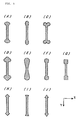
- Each section of the inductor via holes 50a to 52d preferably has an arbitrary shape, and in addition to the shape shown in Fig. 2, as shown in portions (A) and (B) of Fig. 5, shapes (A) a case in which the major axis of an ellipse is preferably substantially perpendicular to the Y direction of the section of a via hole and (B) a case in which the minor axis of an ellipse is substantially perpendicular to the Y direction of the section of a via hole) that each have elliptic ends may be used. Otherwise, shapes that have bifoliate ends and trifoliate ends as shown in portions (C) and (D) of Fig.
- a shape that has a longitudinal constriction as shown in Fig. 5(E) may be used.
- shapes may be used that have octagonal ends, square ends, parallelogramic ends, inverse triangular ends, and equilaterally triangular ends.
- a laminated LC filter 81 according to a second preferred embodiment of the present invention is identical to the LC filter 41 according to the first preferred embodiment, except for inductor via holes 83a to 83d, 84a to 84d, and 85a to 85d.
- the inductor via holes 83a to 83d have an advantage in that they are easy to produce because each section shape on the X-Y plane of them is linear and simplified.
- the inductor via holes 83a to 83d, 84a to 84d, and 85a to 85d, which are arranged in the X-direction of the X-Y plane, are successively connected in a direction (the Z direction) in which insulating sheets 42 to 45 are stacked to define columnar inductors L1, L2, and L3.
- the axial direction of the inductors L1 to L3 is substantially perpendicular to surfaces of the sheets 42 to 45.
- each section of the inductor via holes 83a to 85d has a Y-direction dimension D1 longer than a X-direction dimension D2 on the X-Y plane.
- This increases each section area of the inductor via holes 83a to 85d without widening the intervals of the adjacent inductors L1 to L3.
- Each section of the inductor via holes 83a to 85d is an arbitrary shape, and in addition to the shape shown in Fig. 7, a shape that has linear ends as shown in portion (A) of Fig. 9, a shape that has spiral ends as shown in portion (B) of Fig. 9, and a shape that has polygonal ends as shown in portion (C) of Fig. 9 may be used. In addition, a shape that has elliptic ends as shown in portion (D) of Fig. 9 may be used.
- the LC-included electronic component according to the present invention is not limited to the foregoing preferred embodiments but may be variously modified with the spirit of the present invention.
- LC components include bandpass filters, low-pass filters, and high-pass filters.
- the LC components may also include duplexers obtained by combining bandpass filters, and duplexers obtained by combining low-pass filters, high-pass filters, and trap circuits, or different types of circuits.
- the LC components include components of a type in which a plurality of filters are built into one laminated unit, such as triplexer and diplexer, and components of a type that have a built-in filter and circuit.
- a diplexer is obtained by combining, a low-pass filter and a high-pass filter.
- a type in which a shield pattern is provided on either the top or bottom of a laminated unit may be used.
- the present invention are not limited to the preferred embodiments. Pre-burned insulating sheets may be used.
- the LC components may be produced using the following process. After using paste insulating material to form an insulating layer by printing or other suitable method, paste conductive material is applied to the surface of the insulating layer to form a conductive pattern and a via hole. Next, by applying paste insulating material, an insulating layer is formed. Similarly, by performing successive application in order, an LC component having a layered structure is obtained.
Landscapes
- Physics & Mathematics (AREA)
- Electromagnetism (AREA)
- Filters And Equalizers (AREA)
- Coils Or Transformers For Communication (AREA)
Abstract
Description
Claims (20)
- An LC-included component comprising:
an LC resonator (Q1,Q2,Q3) including at least one inductor (L1,L2,L3) and at least one capacitor (C1,C2,C3), said at least one inductor (L1,L2,L3) and said at least one capacitor (C1,C2,C3) provided in a laminated unit defined by stacked insulating layers (42,43,44,45,46,47,48), wherein:said at least one inductor (L1,L2,L3) is defined by via holes (50a-50d,51a-51d,52a-52d,83a-83d,84a-84d,85a-85d = 1 ○ ) successively connected in a stacking direction (Z) in which the insulating layers (42-48) are stacked; andeach of said via holes 1 ○ having a section shape on an X-Y plane that is substantially perpendicular to said stacking direction such that a dimension in the X direction (Z) differs from a dimension in the Y direction. - An LC-included component according to Claim 1, wherein said via holes 1 ○ are arranged in the X direction of said X-Y plane, and the dimension in the Y direction of said via holes 1 ○ is greater than the dimension of said via holes 1 ○ in the X direction.
- An LC-included component according to Claim 2, wherein the section shape on said X-Y plane of each of said via holes (50a-50d,51a-51d,52a-52d) is configured such that each of two ends in the Y direction is wider than the width of the central portion of the shape.
- An LC-included component according to any of Claims 1 to 3, wherein input and output terminals (p1,p2) which are connected to said via holes 1 ○ are provided at both ends of said laminated unit in the X direction.
- An LC-included component according to any of Claims 1 to 4, wherein said LC-included component is a laminated LC filter.
- An LC-included component according to any of Claims 1 to 5, wherein the Y direction of said via holes 1 ○ is about one to about four times greater than the dimension of said via holes 1 ○ in the X direction.
- An LC-included component according to any of Claims 1 to 6, wherein said at least one capacitor (C1,C2,C3) is defined by a capacitor pattern (53,54,55) opposed to a shield pattern (65), with one of said insulating layers (46,47) provided therebetween.
- An LC-included component according to any of claims 1, wherein each of said via holes has a substantially ellipse shape.
- An LC-included component according to claim 3, wherein said two ends of each of said via holes (50a-50d,51a-51d,52a-52d = 2 ○) have a substantially octagonal shape.
- An LC-included component according to claim 3, wherein each of said via holes 2 ○ includes substantially circular ends and linear central portions.
- A method of manufacturing an LC-included component comprising:providing an LC resonator (Q1,Q2,Q3) including at least one inductor (L1,L2,L3) and at least one capacitor (C1,C2,C3), said at least one inductor (L1,L2,L3) and said at least one capacitor (C1,C2,C3) provided in a laminated unit defined by stacked insulating layers (42-48);forming via holes 1 ○ in said insulating layers (42-48) to define said at least one inductor (L1,L2,L3) such that said via holes 1 ○ are successively connected in a stacking direction (Z) in which the insulating layers (42-48) are stacked; andconfiguring each of said via holes 1 ○ to have a section shape on an X-Y plane that is substantially perpendicular to said stacking direction (Z) such that a dimension in the X direction differs from a dimension in the Y direction.
- A method of manufacturing an LC-included component according to Claim 11, further comprising the steps of arranging said via holes 1 ○ in the X direction of said X-Y plane, and configuring said via holes 1 ○ such that the dimension in the Y direction of said via holes 1 ○ is greater than the dimension of said via holes 1 ○ in the X direction.
- A method of manufacturing an LC-included component according to Claim 12, wherein the section shape on said X-Y plane of each of said via holes 2 ○ is configured such that each of two ends in the Y direction is wider than the width of the central portion of the shape.
- A method of manufacturing an LC-included component according to any of Claims 11-13, further comprising providing input and output terminals (P1,P2) at both ends of said laminated unit in the X direction and connecting said input and output terminals (P1,P2) to said via holes 1 ○.
- A method of manufacturing an LC-included component according to any Claims 11 to 14, wherein said LC-included component is a laminated LC filter.
- A method of manufacturing an LC-included component according to any of Claims 11 to 15, wherein the Y direction of said via holes 1 ○ is about one to about four times greater than the dimension of said via holes 1 ○ in the X direction.
- A method of manufacturing an LC-included component according to any of Claims 11 to 16, further comprising the step of forming said at least one capacitor (C1,C2,C3) by forming a capacitor pattern (53,54,55) opposed to a shield pattern (65), with one of said insulating layers (46,47) provided therebetween.
- A method of manufacturing an LC-included component according to claim 11, wherein each of said via holes has a substantially ellipse shape.
- A method of manufacturing an LC-included component according to claim 13, wherein said two ends of each of said via holes 2 ○ have a substantially octagonal shape.
- A method of manufacturing an LC-included component according to claim 13, wherein each of said via holes 2 ○ includes substantially circular ends and linear central portions.
Applications Claiming Priority (2)
| Application Number | Priority Date | Filing Date | Title |
|---|---|---|---|
| JP2000131447A JP3494120B2 (en) | 2000-04-28 | 2000-04-28 | Laminated LC parts |
| JP2000131447 | 2000-04-28 |
Publications (3)
| Publication Number | Publication Date |
|---|---|
| EP1150375A2 true EP1150375A2 (en) | 2001-10-31 |
| EP1150375A3 EP1150375A3 (en) | 2003-03-12 |
| EP1150375B1 EP1150375B1 (en) | 2009-08-05 |
Family
ID=18640343
Family Applications (1)
| Application Number | Title | Priority Date | Filing Date |
|---|---|---|---|
| EP01108615A Expired - Lifetime EP1150375B1 (en) | 2000-04-28 | 2001-04-05 | LC-included electronic component |
Country Status (5)
| Country | Link |
|---|---|
| US (1) | US6583686B2 (en) |
| EP (1) | EP1150375B1 (en) |
| JP (1) | JP3494120B2 (en) |
| CN (1) | CN1188928C (en) |
| DE (1) | DE60139439D1 (en) |
Families Citing this family (8)
| Publication number | Priority date | Publication date | Assignee | Title |
|---|---|---|---|---|
| JP2003124769A (en) * | 2001-08-09 | 2003-04-25 | Murata Mfg Co Ltd | Lc filter circuit, laminated lc filter, multiplexer and radio communication device |
| US7002434B2 (en) * | 2004-03-16 | 2006-02-21 | Chi Mei Communication Systems, Inc. | Lumped-element transmission line in multi-layered substrate |
| JP4596892B2 (en) * | 2004-11-18 | 2010-12-15 | 京セラ株式会社 | Multilayer capacitor |
| US9166564B2 (en) * | 2010-02-04 | 2015-10-20 | Hittite Microwave Corporation | Wideband analog bandpass filter |
| JPWO2011148819A1 (en) * | 2010-05-28 | 2013-07-25 | 日本碍子株式会社 | Impedance matching element |
| KR101444555B1 (en) * | 2012-12-27 | 2014-09-24 | 삼성전기주식회사 | Band pass filter |
| CN114128141B (en) * | 2019-07-09 | 2025-08-12 | 株式会社村田制作所 | LC filter |
| US11942911B2 (en) | 2021-02-18 | 2024-03-26 | Nuvoton Technology Corporation Japan | Radio-frequency power amplifier device |
Family Cites Families (9)
| Publication number | Priority date | Publication date | Assignee | Title |
|---|---|---|---|---|
| JPH08288142A (en) * | 1995-04-11 | 1996-11-01 | Murata Mfg Co Ltd | Inductor and composite component with built-in inductor |
| JP3127792B2 (en) * | 1995-07-19 | 2001-01-29 | 株式会社村田製作所 | LC resonator and LC filter |
| JP3106942B2 (en) * | 1995-12-28 | 2000-11-06 | 株式会社村田製作所 | LC resonance components |
| JP3501327B2 (en) * | 1995-12-28 | 2004-03-02 | 株式会社村田製作所 | LC resonance components |
| JPH09205018A (en) * | 1996-01-24 | 1997-08-05 | Murata Mfg Co Ltd | Laminated inductor built-in electronic component |
| JPH09219315A (en) * | 1996-02-08 | 1997-08-19 | Murata Mfg Co Ltd | Inductor built-in electronic component |
| JP3164000B2 (en) * | 1996-12-11 | 2001-05-08 | 株式会社村田製作所 | Multilayer inductor |
| JP2000165171A (en) * | 1998-11-30 | 2000-06-16 | Murata Mfg Co Ltd | Lc resonator component and lc filter |
| JP2001136045A (en) * | 1999-08-23 | 2001-05-18 | Murata Mfg Co Ltd | Layered composite electronic component |
-
2000
- 2000-04-28 JP JP2000131447A patent/JP3494120B2/en not_active Expired - Fee Related
-
2001
- 2001-04-05 EP EP01108615A patent/EP1150375B1/en not_active Expired - Lifetime
- 2001-04-05 DE DE60139439T patent/DE60139439D1/en not_active Expired - Lifetime
- 2001-04-17 US US09/836,592 patent/US6583686B2/en not_active Expired - Lifetime
- 2001-04-28 CN CNB011176059A patent/CN1188928C/en not_active Expired - Fee Related
Also Published As
| Publication number | Publication date |
|---|---|
| US20010035803A1 (en) | 2001-11-01 |
| CN1188928C (en) | 2005-02-09 |
| JP2001313536A (en) | 2001-11-09 |
| JP3494120B2 (en) | 2004-02-03 |
| CN1322030A (en) | 2001-11-14 |
| DE60139439D1 (en) | 2009-09-17 |
| EP1150375B1 (en) | 2009-08-05 |
| US6583686B2 (en) | 2003-06-24 |
| EP1150375A3 (en) | 2003-03-12 |
Similar Documents
| Publication | Publication Date | Title |
|---|---|---|
| US8947175B2 (en) | Low-pass filter | |
| US6727782B2 (en) | Multilayered LC composite component and method for manufacturing the same | |
| US6542052B2 (en) | Monolithic LC components | |
| US6504451B1 (en) | Multi-layered LC composite with a connecting pattern capacitively coupling inductors to ground | |
| US6529102B2 (en) | LC filter circuit and laminated type LC filter | |
| US8169288B2 (en) | Electronic component and method for making the same | |
| US6529101B2 (en) | Multilayered LC filter | |
| US6587020B2 (en) | Multilayer LC composite component with ground patterns having corresponding extended and open portions | |
| JP2001085227A (en) | Laminated lc resonator and filter thereof | |
| US6521976B2 (en) | Multilayer LC composite component | |
| EP1150375B1 (en) | LC-included electronic component | |
| KR100456040B1 (en) | Monolithic electronic component | |
| US9178484B2 (en) | Filter | |
| US6424236B1 (en) | Stacked LC filter with a pole-adjusting electrode facing resonator coupling patterns | |
| EP1083620A2 (en) | Monolithic LC resonator and monolithic LC filter | |
| US6831530B2 (en) | Monolithic LC filter with enhanced magnetic coupling between resonator inductors | |
| JPH066105A (en) | Band pass filter | |
| KR20150112891A (en) | Filtering circuit with slot line resonators | |
| US5365208A (en) | Microwave stripline filter formed from a pair of dielectric substrates | |
| JPH0756857B2 (en) | LC composite parts | |
| JPH10116752A (en) | Lc filter component | |
| JPH0918202A (en) | Multilayer dielectric filter and method of manufacturing the same | |
| JPH09181550A (en) | Stacked noise filter | |
| JP2006311506A (en) | LC filter and multiple LC filter | |
| JPH11163603A (en) | Laminated filter |
Legal Events
| Date | Code | Title | Description |
|---|---|---|---|
| PUAI | Public reference made under article 153(3) epc to a published international application that has entered the european phase |
Free format text: ORIGINAL CODE: 0009012 |
|
| 17P | Request for examination filed |
Effective date: 20010405 |
|
| AK | Designated contracting states |
Kind code of ref document: A2 Designated state(s): AT BE CH CY DE DK ES FI FR GB GR IE IT LI LU MC NL PT SE TR |
|
| AX | Request for extension of the european patent |
Free format text: AL;LT;LV;MK;RO;SI |
|
| PUAL | Search report despatched |
Free format text: ORIGINAL CODE: 0009013 |
|
| RIC1 | Information provided on ipc code assigned before grant |
Ipc: 7H 01P 1/203 A Ipc: 7H 03H 7/01 B |
|
| AK | Designated contracting states |
Kind code of ref document: A3 Designated state(s): AT BE CH CY DE DK ES FI FR GB GR IE IT LI LU MC NL PT SE TR |
|
| AX | Request for extension of the european patent |
Extension state: AL LT LV MK RO SI |
|
| AKX | Designation fees paid |
Designated state(s): DE FR GB |
|
| RAP1 | Party data changed (applicant data changed or rights of an application transferred) |
Owner name: MURATA MANUFACTURING CO., LTD. |
|
| 17Q | First examination report despatched |
Effective date: 20071213 |
|
| GRAP | Despatch of communication of intention to grant a patent |
Free format text: ORIGINAL CODE: EPIDOSNIGR1 |
|
| GRAS | Grant fee paid |
Free format text: ORIGINAL CODE: EPIDOSNIGR3 |
|
| GRAA | (expected) grant |
Free format text: ORIGINAL CODE: 0009210 |
|
| AK | Designated contracting states |
Kind code of ref document: B1 Designated state(s): DE FR GB |
|
| REG | Reference to a national code |
Ref country code: GB Ref legal event code: FG4D |
|
| REF | Corresponds to: |
Ref document number: 60139439 Country of ref document: DE Date of ref document: 20090917 Kind code of ref document: P |
|
| PLBE | No opposition filed within time limit |
Free format text: ORIGINAL CODE: 0009261 |
|
| STAA | Information on the status of an ep patent application or granted ep patent |
Free format text: STATUS: NO OPPOSITION FILED WITHIN TIME LIMIT |
|
| 26N | No opposition filed |
Effective date: 20100507 |
|
| GBPC | Gb: european patent ceased through non-payment of renewal fee |
Effective date: 20100405 |
|
| REG | Reference to a national code |
Ref country code: FR Ref legal event code: ST Effective date: 20101230 |
|
| PG25 | Lapsed in a contracting state [announced via postgrant information from national office to epo] |
Ref country code: GB Free format text: LAPSE BECAUSE OF NON-PAYMENT OF DUE FEES Effective date: 20100405 |
|
| PG25 | Lapsed in a contracting state [announced via postgrant information from national office to epo] |
Ref country code: FR Free format text: LAPSE BECAUSE OF NON-PAYMENT OF DUE FEES Effective date: 20100430 |
|
| PGFP | Annual fee paid to national office [announced via postgrant information from national office to epo] |
Ref country code: DE Payment date: 20180420 Year of fee payment: 18 |
|
| REG | Reference to a national code |
Ref country code: DE Ref legal event code: R119 Ref document number: 60139439 Country of ref document: DE |
|
| PG25 | Lapsed in a contracting state [announced via postgrant information from national office to epo] |
Ref country code: DE Free format text: LAPSE BECAUSE OF NON-PAYMENT OF DUE FEES Effective date: 20191101 |