EP1150353A2 - Using lightly doped resistor for output stage electrostatic discharge protection - Google Patents
Using lightly doped resistor for output stage electrostatic discharge protection Download PDFInfo
- Publication number
- EP1150353A2 EP1150353A2 EP01303801A EP01303801A EP1150353A2 EP 1150353 A2 EP1150353 A2 EP 1150353A2 EP 01303801 A EP01303801 A EP 01303801A EP 01303801 A EP01303801 A EP 01303801A EP 1150353 A2 EP1150353 A2 EP 1150353A2
- Authority
- EP
- European Patent Office
- Prior art keywords
- ions
- implanting
- region
- kev
- resistor
- Prior art date
- Legal status (The legal status is an assumption and is not a legal conclusion. Google has not performed a legal analysis and makes no representation as to the accuracy of the status listed.)
- Withdrawn
Links
- 150000002500 ions Chemical class 0.000 claims abstract description 31
- 239000000758 substrate Substances 0.000 claims abstract description 15
- 238000004519 manufacturing process Methods 0.000 claims abstract description 9
- XUIMIQQOPSSXEZ-UHFFFAOYSA-N Silicon Chemical compound [Si] XUIMIQQOPSSXEZ-UHFFFAOYSA-N 0.000 claims abstract description 7
- 229910052710 silicon Inorganic materials 0.000 claims abstract description 7
- 239000010703 silicon Substances 0.000 claims abstract description 7
- 238000000034 method Methods 0.000 claims description 21
- -1 phosphorous ions Chemical class 0.000 claims description 21
- 229910052785 arsenic Inorganic materials 0.000 claims description 7
- 229910052796 boron Inorganic materials 0.000 claims description 7
- 230000000873 masking effect Effects 0.000 claims description 3
- RQNWIZPPADIBDY-UHFFFAOYSA-N arsenic atom Chemical compound [As] RQNWIZPPADIBDY-UHFFFAOYSA-N 0.000 claims description 2
- 238000000151 deposition Methods 0.000 claims 2
- 238000005468 ion implantation Methods 0.000 description 8
- 230000015556 catabolic process Effects 0.000 description 6
- 238000005229 chemical vapour deposition Methods 0.000 description 5
- 239000007943 implant Substances 0.000 description 5
- 238000002955 isolation Methods 0.000 description 4
- 229910021332 silicide Inorganic materials 0.000 description 4
- FVBUAEGBCNSCDD-UHFFFAOYSA-N silicide(4-) Chemical compound [Si-4] FVBUAEGBCNSCDD-UHFFFAOYSA-N 0.000 description 4
- BOTDANWDWHJENH-UHFFFAOYSA-N Tetraethyl orthosilicate Chemical compound CCO[Si](OCC)(OCC)OCC BOTDANWDWHJENH-UHFFFAOYSA-N 0.000 description 3
- 230000003647 oxidation Effects 0.000 description 3
- 238000007254 oxidation reaction Methods 0.000 description 3
- 229910052698 phosphorus Inorganic materials 0.000 description 3
- 239000011574 phosphorus Substances 0.000 description 3
- ZOXJGFHDIHLPTG-UHFFFAOYSA-N Boron Chemical compound [B] ZOXJGFHDIHLPTG-UHFFFAOYSA-N 0.000 description 2
- OAICVXFJPJFONN-UHFFFAOYSA-N Phosphorus Chemical compound [P] OAICVXFJPJFONN-UHFFFAOYSA-N 0.000 description 2
- 230000015572 biosynthetic process Effects 0.000 description 2
- 238000002513 implantation Methods 0.000 description 2
- QVGXLLKOCUKJST-UHFFFAOYSA-N atomic oxygen Chemical compound [O] QVGXLLKOCUKJST-UHFFFAOYSA-N 0.000 description 1
- 238000005530 etching Methods 0.000 description 1
- 239000012212 insulator Substances 0.000 description 1
- 239000000463 material Substances 0.000 description 1
- 229910052751 metal Inorganic materials 0.000 description 1
- 239000002184 metal Substances 0.000 description 1
- 238000012986 modification Methods 0.000 description 1
- 230000004048 modification Effects 0.000 description 1
- 229910021421 monocrystalline silicon Inorganic materials 0.000 description 1
- 229910052760 oxygen Inorganic materials 0.000 description 1
- 239000001301 oxygen Substances 0.000 description 1
- 239000004065 semiconductor Substances 0.000 description 1
- 238000000926 separation method Methods 0.000 description 1
Images


Classifications
-
- H—ELECTRICITY
- H10—SEMICONDUCTOR DEVICES; ELECTRIC SOLID-STATE DEVICES NOT OTHERWISE PROVIDED FOR
- H10D—INORGANIC ELECTRIC SEMICONDUCTOR DEVICES
- H10D84/00—Integrated devices formed in or on semiconductor substrates that comprise only semiconducting layers, e.g. on Si wafers or on GaAs-on-Si wafers
- H10D84/01—Manufacture or treatment
- H10D84/0123—Integrating together multiple components covered by H10D12/00 or H10D30/00, e.g. integrating multiple IGBTs
- H10D84/0126—Integrating together multiple components covered by H10D12/00 or H10D30/00, e.g. integrating multiple IGBTs the components including insulated gates, e.g. IGFETs
- H10D84/0165—Integrating together multiple components covered by H10D12/00 or H10D30/00, e.g. integrating multiple IGBTs the components including insulated gates, e.g. IGFETs the components including complementary IGFETs, e.g. CMOS devices
- H10D84/0167—Manufacturing their channels
-
- H—ELECTRICITY
- H10—SEMICONDUCTOR DEVICES; ELECTRIC SOLID-STATE DEVICES NOT OTHERWISE PROVIDED FOR
- H10D—INORGANIC ELECTRIC SEMICONDUCTOR DEVICES
- H10D84/00—Integrated devices formed in or on semiconductor substrates that comprise only semiconducting layers, e.g. on Si wafers or on GaAs-on-Si wafers
-
- H—ELECTRICITY
- H10—SEMICONDUCTOR DEVICES; ELECTRIC SOLID-STATE DEVICES NOT OTHERWISE PROVIDED FOR
- H10D—INORGANIC ELECTRIC SEMICONDUCTOR DEVICES
- H10D84/00—Integrated devices formed in or on semiconductor substrates that comprise only semiconducting layers, e.g. on Si wafers or on GaAs-on-Si wafers
- H10D84/01—Manufacture or treatment
- H10D84/02—Manufacture or treatment characterised by using material-based technologies
- H10D84/03—Manufacture or treatment characterised by using material-based technologies using Group IV technology, e.g. silicon technology or silicon-carbide [SiC] technology
- H10D84/038—Manufacture or treatment characterised by using material-based technologies using Group IV technology, e.g. silicon technology or silicon-carbide [SiC] technology using silicon technology, e.g. SiGe
-
- H—ELECTRICITY
- H10—SEMICONDUCTOR DEVICES; ELECTRIC SOLID-STATE DEVICES NOT OTHERWISE PROVIDED FOR
- H10D—INORGANIC ELECTRIC SEMICONDUCTOR DEVICES
- H10D89/00—Aspects of integrated devices not covered by groups H10D84/00 - H10D88/00
- H10D89/60—Integrated devices comprising arrangements for electrical or thermal protection, e.g. protection circuits against electrostatic discharge [ESD]
- H10D89/601—Integrated devices comprising arrangements for electrical or thermal protection, e.g. protection circuits against electrostatic discharge [ESD] for devices having insulated gate electrodes, e.g. for IGFETs or IGBTs
- H10D89/911—Integrated devices comprising arrangements for electrical or thermal protection, e.g. protection circuits against electrostatic discharge [ESD] for devices having insulated gate electrodes, e.g. for IGFETs or IGBTs using passive elements as protective elements
Definitions
- This invention relates to electrostatic discharge protection for CMOS integrated circuits, and specifically to the provision of a lightly doped region forming a resistor in an active region of such an integrated circuit.
- CMOS transistors particularly those having longer channel lengths
- ESD electrostatic discharge
- a drain junction may be separated with local oxidation of silicon (LOCOS) techniques at the edge of an n - well to increase the uniformity of triggering of positive ESD events to the output stage, however, the ESD properties of pMOS devices of the output CMOS inverter have not been improved, and there is no known ESD protection for a pMOS device.
- LOCOS local oxidation of silicon
- n - well resistor providing ESD protection for semiconductor devices has been described by G. Notermans, "On the use of n - well resistors for uniform triggering of ESD protection elements," EOS/ESD Symposium Proceedings, page 221, 1997.
- a method of fabricating a CMOS device having improved electrostatic discharge protection properties includes preparing a silicon substrate; forming an n - well for a pMOS active region; forming a p - well for an nMOS active region; and implanting ions to form a lightly doped drain series resistor in at least one of the active regions.
- An electrostatic discharge protection structure for use in a CMOS device having a pMOST and an nMOST therein includes an electrostatic triggering structure to uniformly trigger both pMOST and nMOST output to protect against positive and negative electrostatic discharge events.
- Another object of the invention is to provide such an EDS structure which is smaller than known ESD structures.
- a further object of the invention is to provide an ESD structure which will be operable with all types of CMOS integrated circuits.
- Yet another object of the invention is :o provide an ESD structure which causes uniform triggering to both nMOS and pMOS output transistors to provide protection for both positive and negative ESD events.
- Still another object of the invention is to provide and ESD structure suitable for use with CMOS devices fabricated on n-type substrates and on p-type substrates.
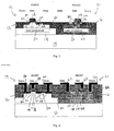
- Figs. 1 - 4 depict successive steps in the fabrication of a device according to a first embodiment of the invention.
- FIG. 5 and 6 depict successive steps in the fabrication of a device according to a second embodiment of the invention.
- the electrostatic discharge (ESD) protection structure of the invention provides an improved and smaller size output protection for CMOS integrated circuits. It provides uniform triggering to both nMOS and pMOS output transistors to provide protection for both positive and negative ESD events.
- the structure may be applied to CMOS devices fabricated on n-type substrates, as well as fabricated on p-type substrates.
- the addition of a series resistance to the drain of the device makes the second breakdown voltage larger than the first breakdown voltage, which provides uniform triggering of the output transistor and uniform ESD current flow. This protects against both positive and negative ESD events at the output of the CMOS integrated circuit.
- the lightly doped (LDD) resistor may be incorporated into any standard CMOS fabrication process, generally, without any additional masking steps or any additional process steps. Only the n + and p + ion implantation mask has to be modified.
- a substrate 10 is prepared for CMOS fabrication.
- Substrate 10 may be a single crystal silicon, a silicon-on-insulator (SOI) substrate, or a separation by implantation of oxygen (SIMOX) substrate.
- Isolation regions 12, 14 and 16 are formed by local oxidation of silicon (LOCOS) or shallow trench isolation (STI), or any other state of the art isolation process, such as mesa for SOI devices.
- LOCOS local oxidation of silicon
- STI shallow trench isolation
- State of the art processes are followed to form an n-well active region 18, which will form an active region for a pMOST 19, and a p-well active region 20, which will form an active region for a nMOST 21.
- Threshold adjustment ion implantation, gate oxidation to form gate oxide layers 22, 24, and gate electrode formation to form gate electrodes 26, 28, are accomplished by any state of the art processes for pMOS transistor 19 and nMOS transistor 21, respectively.
- the term "pMOST” as used herein refers to a pMOS transistor.
- the term “nMOST” as used herein refers to an nMOS transistor.
- a mask (not shown) is applied to protect nMOS region 21.
- Phosphorus or arsenic ions are implanted to form n-type LDD region 30 in nMOS 21.
- arsenic ions are implanted at an energy of between 20 keV and 50 keV (if phosphorous ions are used, the implant energy range is preferably 10 keV to 50 keV), at a dose of between 1 x 10 12 cm -2 and 1 x 10 14 cm -2 , resulting in an ion concentration of between 1 x 10 18 cm -3 and 1 x 10 20 cm -3 .
- BF 2 ions are implanted at an energy of between 20 keV and 50 keV (if boron ions are used, the implant energy range is preferably 10 keV to 50 keV), at a dose of between 1 x 10 12 cm -2 and 1 x 10 14 cm -2 , resulting in an ion concentration of between 1 x 10 18 cm -3 and 1 x 10 20 cm -3 .
- a thin oxide is deposited by chemical vapor deposition (CVD) and anisotropically etched to form a sidewall oxide 34. 36 about gate electrodes 26, 28, respectively.
- n + ion implantation mask 38, 40 is applied prior to phosphorus or arsenic n + ion implantation.
- Mask 38 covers all of pMOS transistor 19 and a portion of what will become a drain region of nMOS transistor 21, as shown in Fig. 2.
- Ion implantation implants n + ions in nMOS 21, forming an nMOS drain 42 and an nMOS source 44.
- Drain 42 and source 44 are formed by implanting arsenic ions at a dose of 1 x 10 15 cm -2 to 5.0 x 10 15 cm -2 at an energy of 20 keV to 50 keV, or, if phosphorus ions are implanted, the implant energy range is preferably 10 keV to 50 keV.
- Source 46 and drain 48 are, in this instance, formed by implanting BF 2 ions at a dose of 1 x 10 15 cm -2 to 5.0 x 10 15 cm -2 at an energy of 20 keV to 50 keV. If boron ions are implanted the implant energy is preferably 10 keV to 50 keV. This mask is then stripped, resulting in the structure depicted in Fig. 3.
- LDD drain series resistors 50, 52 for nMOS region 21 and pMOS region 19, respectively, are shown.
- This drain series resistance provides a voltage drop, which prevents the second breakdown of a local weak point before the other portion of the drain breakdown occurs.
- the addition of a series resistance to the drain of the device makes the second breakdown voltage larger than the first breakdown voltage, which provides uniform triggering of the output transistor and uniform ESD current flow. This protects against both positive and negative ESD events at the output of the CMOS integrated circuit. Therefore, a uniform ESD current flow is possible.
- Drains series resistors 50, 52 comprise what is referred to herein as an electrostatic triggering structure to uniformly trigger both pMOST and nMOST output to protect against positive and negative electrostatic discharge events.
- n + gate is used as an example.
- a thick layer of oxide 54 such as tetraethylorthosilicate (TEOS) is deposited, contact holes opened and first metal deposited and etched, forming, for pMOST 19, a source electrode 56, a gate electrode 58, and a drain electrode 60.
- nMOST 21 has a drain electrode 62, a gate electrode 64 and a source electrode 66 operatively connected thereto.
- nLDD resistor 50 is formed in drain 42 of nMOS 21 and pLDD resistor 52 is formed in drain 48 of pMOS 19, the ESD structure will work even if only a single nLDD resistor is added to the drain of the nMOST or only a pLDD resistor is added to the drain of the pMOST.
- This embodiment may also be used with SOI structures.
- a substrate 70 has isolation regions 72, 74 and 76 formed therein.
- An n - well active region 78 is formed, for a pMOS region 79, which will become a pMOST.
- a p - well active region 80 is formed, for an nMOS region 81, which will become a nMOST.
- An oxide layer 82, 84 is deposited, and a gate electrode 86, 88 is also deposited, for pMOS region 79 and nMOS region 81, respectively.
- a pLDD region 90 and an nLDD region 92 arc formed for pMOS region 79 and nMOS region 81, respectively, and a gate sidewall 94, 96 is deposited.
- Selective silicidation takes place on n + and p + areas, but is not allowed to occur on the LDD resistor areas. This may be achieved by adding masks 98, 100, prior to the etching of gate sidewall oxide 94, 96, after LDD ion implantation and CVD of the sidewall oxides. The sidewall oxide is etched and resist removed. There will be oxide on the surface of the LDD resistor regions. Because the resistors are covered by oxide, these regions will not be silicided. If selective CVD silicide is used no silicide can be deposited onto these region.
- Silicide regions 102, 104 are deposited by CVD on pMOS region 79 and nMOS region 81, respectively. Appropriate ions, as previously described, are implanted to form drains 106, 108 and sources 110, 112, for pMOS region 79 and nMOS region 81, respectively. This results in the formation of LDD resistors 114, 116. An oxide layer 118, such as TEOS is deposited and etched to form contact holes for source electrodes 120, 126, gate electrodes 122, 128, and drain electrodes 124, 130, for pMOST 79 and nMOST 81, respectively. The final structure for silicide process is shown in Fig. 6.
Landscapes
- Semiconductor Integrated Circuits (AREA)
- Metal-Oxide And Bipolar Metal-Oxide Semiconductor Integrated Circuits (AREA)
- Insulated Gate Type Field-Effect Transistor (AREA)
Abstract
Description
Claims (16)
- A method of fabricating a CMOS device having improved electrostatic discharge protection properties, comprising:preparing a silicon substrate;forming an n-well for a pMOS active region;forming a p-well for an nMOS active region; andimplanting ions to form a lightly doped drain series resistor in at least one of the active regions.
- The method of claim 1 wherein said implanting includes implanting n-type ions in the nMOS active region to form an nLDD region and implanting p-type ions in the pMOS active region to form a pLDD region.
- The method of claim 2 wherein said implanting n-type ions includes implanting ions taken from the group of ions consisting of phosphorous ions and arsenic at an energy of between 10 keV and 50 keV, at a dose of between 1 x 1012 cm-2 and 1 x 1014 cm-2.
- The method of claim 2 wherein said implanting p-type ions includes implanting ions taken from the group of ions consisting of boron ions and BF2 ions at an energy of between 10 keV and 50 keV, at a dose of between 1 x 1012 cm-2 and 1 x 1014 cm-2.
- The method of claim 2 which further includes masking portions of the nLDD region and pLDD region over the area of the LDD drain series resistors and siliciding the nonmasked portions of the active regions.
- The method of claim 1 which further includes forming an oxide layer over the active regions, implanting ions to form drain and source regions in each of the active regions, depositing an insulating layer over the structure, and metallizing the structure.
- A method of fabricating a CMOS device having improved electrostatic discharge protection properties, comprising:preparing a silicon substrate;forming an n-well for a pMOS active region;forming a p-well for an nMOS active region; andforming a gate oxide layer over the active regions,forming a gate on the gate oxide layer;implanting ions to form a lightly doped drain series resistor in at least one of the active regions;implanting ions to form drain and source regions in each of the active regions, depositing an insulating layer over the structure; andmetallizing the structure.
- The method of claim 7 herein said implanting ions to form a lightly doped drain series resistor includes implanting n-type ions in the nMOS active region to form an nLDD region and implanting p-type ions in the pMOS active region to form a pLDD region.
- The method of claim 8 wherein said implanting n-type ions includes implanting ions taken from the group of ions consisting of phosphorous ions and arsenic ions at an energy of between 10 keV and 50 keV, at a dose of between 1 x 1012 cm-2 and 1 x 1014 cm-2.
- The method of claim 8 wherein said planting p-type ions includes implanting ions taken from the group of ions consisting of boron ions and BF2 ions at an energy of between 10 keV and 50 keV, at a dose of between 1 x 1012 cm-2 and 1 x 1014 cm-2.
- The method of claim 7 which further includes masking portions of the nLDD region and pLDD region over the area of the LDD drain series resistors and siliciding the nonmasked portions of the active regions.
- In a CMOS device having a pMOST and an nMOST therein, an electrostatic discharge protection structure comprising:
an electrostatic triggering structure to uniformly trigger both pMOST and nMOST output to protect against positive and negative electrostatic discharge events. - The CMOS device of claim 12 wherein said electrostatic triggering structure includes a lightly doped resister in series with a drain structure of at least one of the transistors.
- The CMOS device of claim 13 which includes a nLDD resistor in the nMOST and a pLDD resistor in the pMOST.
- The CMOS device of claim 14 wherein said nLDD resistor has a concentration of ions taken from the group of ions consisting of phosphorous ions and arsenic ions of between about 1 x 1018 cm-3 and 1 x 1020 cm-3.
- The CMOS device of claim 14 wherein said pLDD resistor has a concentration of ions taken from the group of ions consisting of boron ions and BF2 ions of between about 1 x 1018 cm-3 and 1 × 1020 cm-3.
Applications Claiming Priority (2)
| Application Number | Priority Date | Filing Date | Title |
|---|---|---|---|
| US55911600A | 2000-04-26 | 2000-04-26 | |
| US559116 | 2000-04-26 |
Publications (2)
| Publication Number | Publication Date |
|---|---|
| EP1150353A2 true EP1150353A2 (en) | 2001-10-31 |
| EP1150353A3 EP1150353A3 (en) | 2005-09-21 |
Family
ID=24232327
Family Applications (1)
| Application Number | Title | Priority Date | Filing Date |
|---|---|---|---|
| EP01303801A Withdrawn EP1150353A3 (en) | 2000-04-26 | 2001-04-26 | Using lightly doped resistor for output stage electrostatic discharge protection |
Country Status (4)
| Country | Link |
|---|---|
| EP (1) | EP1150353A3 (en) |
| JP (1) | JP2001358227A (en) |
| KR (1) | KR100429520B1 (en) |
| TW (1) | TW517373B (en) |
Cited By (1)
| Publication number | Priority date | Publication date | Assignee | Title |
|---|---|---|---|---|
| CN107170739A (en) * | 2017-07-12 | 2017-09-15 | 深圳市航顺芯片技术研发有限公司 | A kind of silicon gate MOS integrated circuit esd protection circuit structure |
Families Citing this family (4)
| Publication number | Priority date | Publication date | Assignee | Title |
|---|---|---|---|---|
| JP2004356583A (en) * | 2003-05-30 | 2004-12-16 | Ngk Spark Plug Co Ltd | Resin wiring board with pins |
| JP2007335463A (en) * | 2006-06-12 | 2007-12-27 | Renesas Technology Corp | Electrostatic discharging protective element, and semiconductor device |
| KR100835282B1 (en) * | 2007-01-23 | 2008-06-05 | 삼성전자주식회사 | Electrostatic discharge protection device |
| JP4844621B2 (en) * | 2008-12-04 | 2011-12-28 | ソニー株式会社 | Transistor-type protection device and semiconductor integrated circuit |
Family Cites Families (6)
| Publication number | Priority date | Publication date | Assignee | Title |
|---|---|---|---|---|
| US5283449A (en) * | 1990-08-09 | 1994-02-01 | Nec Corporation | Semiconductor integrated circuit device including two types of MOSFETS having source/drain region different in sheet resistance from each other |
| US5498892A (en) * | 1993-09-29 | 1996-03-12 | Ncr Corporation | Lightly doped drain ballast resistor |
| JP2715929B2 (en) * | 1994-08-18 | 1998-02-18 | 日本電気株式会社 | Semiconductor integrated circuit device |
| US5602404A (en) * | 1995-01-18 | 1997-02-11 | National Semiconductor Corporation | Low voltage triggering silicon controlled rectifier structures for ESD protection |
| US6051458A (en) * | 1998-05-04 | 2000-04-18 | Taiwan Semiconductor Manufacturing Company | Drain and source engineering for ESD-protection transistors |
| US6211001B1 (en) * | 1998-07-24 | 2001-04-03 | Sharp Laboratories Of America, Inc. | Electrostatic discharge protection for salicided devices and method of making same |
-
2001
- 2001-04-24 JP JP2001126769A patent/JP2001358227A/en active Pending
- 2001-04-26 TW TW090109994A patent/TW517373B/en not_active IP Right Cessation
- 2001-04-26 EP EP01303801A patent/EP1150353A3/en not_active Withdrawn
- 2001-04-26 KR KR10-2001-0022660A patent/KR100429520B1/en not_active Expired - Fee Related
Cited By (1)
| Publication number | Priority date | Publication date | Assignee | Title |
|---|---|---|---|---|
| CN107170739A (en) * | 2017-07-12 | 2017-09-15 | 深圳市航顺芯片技术研发有限公司 | A kind of silicon gate MOS integrated circuit esd protection circuit structure |
Also Published As
| Publication number | Publication date |
|---|---|
| EP1150353A3 (en) | 2005-09-21 |
| KR100429520B1 (en) | 2004-05-03 |
| TW517373B (en) | 2003-01-11 |
| JP2001358227A (en) | 2001-12-26 |
| KR20010098909A (en) | 2001-11-08 |
Similar Documents
| Publication | Publication Date | Title |
|---|---|---|
| KR100392901B1 (en) | Method of manufacturing an asymmetric slightly doped drain (LCD) MOS device | |
| JP4811895B2 (en) | Semiconductor device and manufacturing method thereof | |
| US7544573B2 (en) | Semiconductor device including MOS field effect transistor having offset spacers or gate sidewall films on either side of gate electrode and method of manufacturing the same | |
| US6096591A (en) | Method of making an IGFET and a protected resistor with reduced processing steps | |
| EP0465045B1 (en) | Method of field effect transistor fabrication for integrated circuits | |
| EP0975023B1 (en) | Method of making electrostatic discharge protected salicided devices | |
| EP1026738B1 (en) | Novel mixed voltage CMOS process for high reliability and high performance core and I/O transistors with reduced mask steps | |
| US6479339B2 (en) | Use of a thin nitride spacer in a split gate embedded analog process | |
| US6583013B1 (en) | Method for forming a mixed voltage circuit having complementary devices | |
| US6051459A (en) | Method of making N-channel and P-channel IGFETs using selective doping and activation for the N-channel gate | |
| US6027964A (en) | Method of making an IGFET with a selectively doped gate in combination with a protected resistor | |
| JP4501183B2 (en) | Manufacturing method of semiconductor device | |
| US6372590B1 (en) | Method for making transistor having reduced series resistance | |
| US6287922B1 (en) | Method for fabricating graded LDD transistor using controlled polysilicon gate profile | |
| EP1150353A2 (en) | Using lightly doped resistor for output stage electrostatic discharge protection | |
| US7598538B2 (en) | ESD protecting circuit and manufacturing method thereof | |
| US7560779B2 (en) | Method for forming a mixed voltage circuit having complementary devices | |
| US6110788A (en) | Surface channel MOS transistors, methods for making the same, and semiconductor devices containing the same | |
| KR100281397B1 (en) | A method of forming an ultra-thin soi electrostatic discharge protection device | |
| US6780700B2 (en) | Method of fabricating deep sub-micron CMOS source/drain with MDD and selective CVD silicide | |
| US6882013B2 (en) | Transistor with reduced short channel effects and method | |
| JP3390336B2 (en) | Semiconductor integrated circuit device and method of manufacturing the same | |
| JP3240991B2 (en) | Semiconductor device and manufacturing method thereof | |
| EP0878833B1 (en) | Process for the selective formation of salicide on active areas of MOS devices | |
| KR20070001593A (en) | Gate Forming Method of Semiconductor Device |
Legal Events
| Date | Code | Title | Description |
|---|---|---|---|
| PUAI | Public reference made under article 153(3) epc to a published international application that has entered the european phase |
Free format text: ORIGINAL CODE: 0009012 |
|
| AK | Designated contracting states |
Kind code of ref document: A2 Designated state(s): AT BE CH CY DE DK ES FI FR GB GR IE IT LI LU MC NL PT SE TR |
|
| AX | Request for extension of the european patent |
Free format text: AL;LT;LV;MK;RO;SI |
|
| PUAL | Search report despatched |
Free format text: ORIGINAL CODE: 0009013 |
|
| AK | Designated contracting states |
Kind code of ref document: A3 Designated state(s): AT BE CH CY DE DK ES FI FR GB GR IE IT LI LU MC NL PT SE TR |
|
| AX | Request for extension of the european patent |
Extension state: AL LT LV MK RO SI |
|
| 17P | Request for examination filed |
Effective date: 20060313 |
|
| AKX | Designation fees paid |
Designated state(s): DE FR GB |
|
| 17Q | First examination report despatched |
Effective date: 20060623 |
|
| STAA | Information on the status of an ep patent application or granted ep patent |
Free format text: STATUS: THE APPLICATION HAS BEEN WITHDRAWN |
|
| 18W | Application withdrawn |
Effective date: 20071204 |