EP1149287B1 - Sensor housing - Google Patents
Sensor housing Download PDFInfo
- Publication number
- EP1149287B1 EP1149287B1 EP00908384A EP00908384A EP1149287B1 EP 1149287 B1 EP1149287 B1 EP 1149287B1 EP 00908384 A EP00908384 A EP 00908384A EP 00908384 A EP00908384 A EP 00908384A EP 1149287 B1 EP1149287 B1 EP 1149287B1
- Authority
- EP
- European Patent Office
- Prior art keywords
- sensor
- housing
- fluid
- baffle
- flow
- Prior art date
- Legal status (The legal status is an assumption and is not a legal conclusion. Google has not performed a legal analysis and makes no representation as to the accuracy of the status listed.)
- Expired - Lifetime
Links
Images


Classifications
-
- G—PHYSICS
- G01—MEASURING; TESTING
- G01N—INVESTIGATING OR ANALYSING MATERIALS BY DETERMINING THEIR CHEMICAL OR PHYSICAL PROPERTIES
- G01N33/00—Investigating or analysing materials by specific methods not covered by groups G01N1/00 - G01N31/00
- G01N33/0004—Gaseous mixtures, e.g. polluted air
- G01N33/0009—General constructional details of gas analysers, e.g. portable test equipment
- G01N33/0011—Sample conditioning
- G01N33/0014—Sample conditioning by eliminating a gas
-
- G—PHYSICS
- G01—MEASURING; TESTING
- G01F—MEASURING VOLUME, VOLUME FLOW, MASS FLOW OR LIQUID LEVEL; METERING BY VOLUME
- G01F1/00—Measuring the volume flow or mass flow of fluid or fluent solid material wherein the fluid passes through a meter in a continuous flow
- G01F1/68—Measuring the volume flow or mass flow of fluid or fluent solid material wherein the fluid passes through a meter in a continuous flow by using thermal effects
- G01F1/684—Structural arrangements; Mounting of elements, e.g. in relation to fluid flow
- G01F1/6842—Structural arrangements; Mounting of elements, e.g. in relation to fluid flow with means for influencing the fluid flow
-
- G—PHYSICS
- G01—MEASURING; TESTING
- G01F—MEASURING VOLUME, VOLUME FLOW, MASS FLOW OR LIQUID LEVEL; METERING BY VOLUME
- G01F1/00—Measuring the volume flow or mass flow of fluid or fluent solid material wherein the fluid passes through a meter in a continuous flow
- G01F1/68—Measuring the volume flow or mass flow of fluid or fluent solid material wherein the fluid passes through a meter in a continuous flow by using thermal effects
- G01F1/684—Structural arrangements; Mounting of elements, e.g. in relation to fluid flow
- G01F1/6845—Micromachined devices
-
- G—PHYSICS
- G01—MEASURING; TESTING
- G01N—INVESTIGATING OR ANALYSING MATERIALS BY DETERMINING THEIR CHEMICAL OR PHYSICAL PROPERTIES
- G01N1/00—Sampling; Preparing specimens for investigation
- G01N1/02—Devices for withdrawing samples
- G01N1/22—Devices for withdrawing samples in the gaseous state
- G01N1/2247—Sampling from a flowing stream of gas
-
- G—PHYSICS
- G01—MEASURING; TESTING
- G01N—INVESTIGATING OR ANALYSING MATERIALS BY DETERMINING THEIR CHEMICAL OR PHYSICAL PROPERTIES
- G01N25/00—Investigating or analyzing materials by the use of thermal means
- G01N25/18—Investigating or analyzing materials by the use of thermal means by investigating thermal conductivity
-
- G—PHYSICS
- G01—MEASURING; TESTING
- G01N—INVESTIGATING OR ANALYSING MATERIALS BY DETERMINING THEIR CHEMICAL OR PHYSICAL PROPERTIES
- G01N25/00—Investigating or analyzing materials by the use of thermal means
- G01N25/20—Investigating or analyzing materials by the use of thermal means by investigating the development of heat, i.e. calorimetry, e.g. by measuring specific heat, by measuring thermal conductivity
- G01N25/48—Investigating or analyzing materials by the use of thermal means by investigating the development of heat, i.e. calorimetry, e.g. by measuring specific heat, by measuring thermal conductivity on solution, sorption, or a chemical reaction not involving combustion or catalytic oxidation
- G01N25/4873—Investigating or analyzing materials by the use of thermal means by investigating the development of heat, i.e. calorimetry, e.g. by measuring specific heat, by measuring thermal conductivity on solution, sorption, or a chemical reaction not involving combustion or catalytic oxidation for a flowing, e.g. gas sample
- G01N25/488—Details
-
- G—PHYSICS
- G01—MEASURING; TESTING
- G01N—INVESTIGATING OR ANALYSING MATERIALS BY DETERMINING THEIR CHEMICAL OR PHYSICAL PROPERTIES
- G01N1/00—Sampling; Preparing specimens for investigation
- G01N1/02—Devices for withdrawing samples
- G01N1/22—Devices for withdrawing samples in the gaseous state
- G01N2001/2285—Details of probe structures
Definitions
- the invention relates to fluid sensors and particularly to microsensors. More particularly it pertains to housing for such sensors.
- Microsensors have one vexing packaging problem. Their space- and cost-saving smallness (in surface area and membrane thickness) makes them vulnerable to occasional impacts with particles.
- the solid particles may destroy the gas-sensitive membrane of the sensor or change its heat transfer features with just a thin coat of sticky particles.
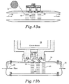
- the liquid ones may have the same effect as the small solids, if a residue stays after re-evaporation. Solutions conceived and implemented to date, may either only provide partial protection and clog after a relatively short service life (screens, Figure 1a) or provide good protection but require costly machining and assembly, and increase response time unacceptably (baffles), see Figures 1a and b.
- US-A-3,720,093 discloses a device for measuring CO 2 concentration in a gas sample, which comprises a thermistor in a detector housing, said housing having a fluid passageway to a sensing cavity, and said thermistor being shielded from the direct impingement of the gas sample by a screen-like 40-mesh brass thimble.
- US-A-5,505,073 discloses a sensor assembly for sensing a fluid medium, which comprises a sensor element within a housing mounted within a S-shaped flow channel between a medium entry aperture and exit aperture, and a shield upstream of the sensor element in the flow direction of the medium.
- WO-A-91/04067 discloses an apparatus for monitoring gas in which a thermistor is provided in a sensing chamber which is in gaseous communication with a gas supply conduit. A baffle is provided to divert a portion of the gas in the conduit into the chamber.
- a sensor housing as defined in the appended claims both protects small, one micrometer-thick sensing structures of thermal microsensors, and facilitates rapid and reliable operation in spite of exposure to forced convection, flow turbulence, dust, droplets and/or condensation.
- thermophysical properties such as thermal conductivity, specific heat, or its derivatives of oxygen demand, heating value, compressibility factor or octane number
- the sensor In order to sense fluid (i.e., gas or liquid) thermophysical properties such as thermal conductivity, specific heat, or its derivatives of oxygen demand, heating value, compressibility factor or octane number, the sensor needs to be in contact with the fluid and be able to reliably sense small changes in the above properties.
- the sensitivity is provided by the design of the sensor chip itself, featuring low mass, large surface-to-volume ratio heating and sensing elements. Long and reliable service requires that the sensor be protected from interference due to settling dust or droplets, as well as from flow (laminar or turbulent). Protection against condensation means that the sensor is designed to recover its sensing performance within a specified short time after coming in contact with liquid condensates. Rapid response means that the sensor chip itself needs to respond quickly to changes in the fluid properties, as well as that the sensor package needs to allow quick transport and replacement of "old” with "new” fluid sample
- aspects of four parameter groups which a designer can adjust to meet the desired sensor performance, include sensor chip design and performance, geometry of the convective transport section of the sensor package, geometry of the convective barrier, and geometry of the diffusion transport section.
- the proposed approach is shown in Figures 4c and 4e.
- the single-stage baffle is shaped to facilitate liquid runoff via the sides, if liquid should get near the sensor chip. It is machined with a set of concentric holes projecting an area around the chip and inhibiting direct splashes from the direction of the fitting to hit the chip. It provides chip protection while allowing diffusional access of fluid to the chip from all sides.
- the disclosed housing for microsensors features a new environmental protection design based on a single-stage, concentric baffle with openings arranged around the protected sensor. It minimizes remaining dead spaces around the sensor (to reduce response time) by filling-in those spaces that are non-essential for fluid diffusion.
- baffle does not need assembly after machining.
- the concentric baffle holes are large enough to make the probability of clogging negligible.
- the response time is five to nine times smaller than that measured with a previous 2-stage, non-concentric baffle (having two offset and opposed D-shaped louvers of Figure 1b).
- the housing orientation relative to external flow direction does not affect the baffle's effectiveness. It is easy to machine, requires no assembly, and barely increases microsensor response time relative to not having a baffle at all.
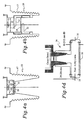
- the sensor housing or package 10 solves harsh environmental problems by providing a sensor 11 with a "microenvironmental” shield or baffle 12, such that forced convection 13 can transport the fluid sample (with dust and droplets) 14 to shield 12. Then diffusivity transports sample 14 between shield 12 and sensor 11.
- Figure 1a shows the principle of housing indicating the protected location of the sensor chip 11 (its magnified cross section is shown in Figure 1c), a generic barrier (such as a screen) shield 12 for protection from convection flows, and transport of fluid sample elements 14 to sensor 11 into a diffusion area 22.
- Figure 1b shows a barrier 15 of a sensor 11, based on an angled path, which avoids a direct line-of-flight between an aerosol from the main flow stream 16 and sensor chip 11, and an incidental 0.63 cm (1/4") NPT fitting 17 to attach sensor 18 to the fluid stream to be monitored.
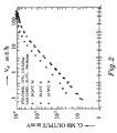
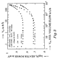
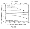
- the rationale for design 18 was derived from measurements, shown in Figures 2 and 3, which display microsensor flow data based on two methods of measurement. Differential and absolute flow sensing, using the same sensor, whereby the heater is controlled to operate at a constant temperature rise above ambient of about 100 degrees Celsius (C), unless indicated otherwise.
- the flow signal is derived from the difference in temperature between the two non-energized (Pt thin-film resistor) sensing elements flanking the central heating element, all of which are more or less influenced by forced convection.
- Figure 3 shows that this influence is delayed for the heater, which consumes a steady power of about 5 mW within ⁇ 0.5% until flow has risen to about 160 L/h, which for the used Venturi nozzle of a 14 mm inside diameter (ID) is equivalent to 28 cm/s.
- Figure 3 shows that this heater power is proportional to thermal conductivity, as we compare the data for CH 4 , C 2 H 6 and N 2 , labeled M, E, and N in Figures 2 and 3.
- the plotted heater power, P can be used to derive thermal conductivity, k, with a linear relationship between heater power and k.
- Typical industrial gas streams range well above the above value of 28 centimeters per second (cm/s), so that some protection of chip 11 as indicated in Figures 1a-1c is needed.
- Response times can be and were measured by recording the transient sensor signals during a switch from one gas to another and back (typically from N 2 to Ar or to CH 4 ), while maintaining a flow of 240 Liters/hour (about 1 gallon/minute) in a pipe of 18 mm (0.71") ID, corresponding to a linear speed of 26.2 cm/s, and with the sensor chip positioned a distance of 24 mm (0.94") away from the pipe center, as in Figure 4d.
- the 240 L/h or 4 L/min requirement was needed to obtain a conservative measure of the response time because under our conditions it was found to decrease somewhat inversely proportional to flow speed.
- Figures 5b and 5c show the effects of flow rates of 600 and 1000 L/h, respectively.
- Figures 6a, 6b and 6c show that gas composition also has an influence on the response time.
- the response times were observed to increase as the N 2 -to-gas switch was made with argon, propane and heptane, from 0.53, 0.94 and 3.5 seconds, respectively. And these increases approximately scale as the inverse of their mass diffusivities of 0.096, 0.039 and 0.016, respectively.
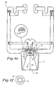
- a single-stage baffle 25 is shaped to facilitate liquid runoff via sides 26, if liquid should get near the sensor chip 11. Second, it is machined with a set of concentric holes 21 projecting an area around sensor chip 11 and inhibiting direct splashes from the direction of the fitting to hit chip 11. Baffle 25 also provides chip protection while allowing diffusional access of fluid to chip 11 from all sides.
- a ring-shaped insert 27 reduces the dead space around chip 11, which may be further cut by means of an epoxy-fill. Insert 27, as shown in figures 4c and 4e, has an outside diameter of about 0.43 cm (0.170 inch.), an inside diameter of about 0.33 cm (0.130 inch.).
- the change in thickness is a straight-line slope from the outside diameter to the inside diameter, with the sloped surface towards baffle 25.
- An inlet 64 of fitting 17 has a radius 65 that tapers down to a radius 19 through the length of the inlet.
- Baffle 25 is at a distance 19 from the inlet entrance of diameter 65. For certain favorable performance, a ratio of diameter 65 to distance 19 is close to or greater than one.
- Baffle 25 is a little curved or convex. It is the barrier of convection lines 13 of flow. Barrier 12, 25 hinders flow lines 13 of convection. After barrier or baffle 12, 25, between the baffle and the sensor, diffusion of fluid 22 takes over the transport job. Baffle 25, 12 keeps the convection of the fluid from sensor 11. Brownian motion takes place between baffle 25, 12 and sensor 11.
- the droplet 39 test shown in figure 8b applies to gas; a liquid 38 is the source of saturated vapor in volume 37, which condenses to droplets 39 which are prevented from impinging sensor 11 by the solid area of baffle 25. For supersonic flows, the hole or holes 21 of the baffle 25 would be very small. Baffle 25 center of solid material should mirror the sensor 11 configuration or area.
- Hole 21 length dampens convection.
- the length-to-diameter ratio of each hole 21 should not exceed one, that is, L/D ⁇ 1 or D/L ⁇ 1.
- Hole 21 walls create friction to inhibit convection.
- the projected volume under the hole 21 area, between the baffle and the sensor, should be about the same as the projected volume under the solid area of baffle 25 between the baffle and sensor.
- Holes 21 should be small enough to prevent passing of convection of the fluid, and the sum of the projected volumes from holes 21 to the sensor 11 side should be no smaller than the projected volume of the solid part of baffle 25.
- Thermal properties include thermal conductivity, specific heat, and thermal diffusivity.
- the distance between baffle 25 and the sensor 11 surface is kept greater than 100 microns, so as to prevent the quenching the thermal process to be measured.
- the aspect ratio of the diameter to length of each hole 21 should be close to one for good response time (D/L ⁇ 1).
- Structure 17 is coned at the input.
- the sensor 11 recess volume 22 is kept as small as possible to minimize diffusion times.
- the ratio of sensor 11 diameter 57 to the recess diameter 19 should be close to one but to allow for baffle openings.
- the area over or under the sensor itself should have no holes 21 or openings in the baffle 25.
- Figure 7 shows the results of sensitivity to flow for designs of Figures 4a, 4b and 4c.
- Figure 4c represents our preferred embodiment, also from the point of view of ease of assembly, whereby the sensor and baffle are machined out of one piece.
- Electronics 28 can be fastened within an enclosure having a cover 29 of Figure 4e.
- o-ring seals 30 are used on the chip holder.
- barrier 25 has six holes 21 having a diameter of about 0.13 cm (0.050 inch.).
- the diameter of a circumference of a perimeter touching the outside edges of holes 21 is about 0.43 cm (0.170 inch,), and diameter 57 of a circumference of a perimeter touching the inside edges of holes 21 is about 0.18 cm (0.070 inch).
- the spacing between adjacent holes 21 is about 0.025 cm (0.010 inch).
- a thickness 75 of barrier 25 at its center is about 0.08 cm (0.030 inch).
- the curvature of baffle 25 is outward towards sensor chip 11.
- the entrance of inlet 64 has a diameter 65 of about 1.09 cm (0.430 inch).
- a length 66 of inlet 64 from the entrance to the center of barrier 25 is about 1.3 cm (0.510 inch.).
- Diameter 19 of barrier 25 at the upper end of inlet 64 is about 0.48 cm (0.190 inch).
- Distance 76 between chips 11 and the center of barrier 25 is about 0.08 cm (0.030 inch.).
- the diameter of chip 11 is about the same as diameter 57 of the solid portion at the center of barrier 25.
- the gas supply from pressurized tanks and regulators was replaced with a shop vacuum pump, the effect of turbulence was striking. Without measurable pressure fluctuations ( ⁇ p ⁇ 0.3 cmWC), the random motion of turbulence enhanced the heat transfer at the site of the chip's sensor elements to the point of simulating the behavior of a fluid with higher than actual thermal conductivity.
- Figure 7 shows that the sensor packages shown in Figure 4a-c, and 4e with convection barriers in the form of a wire screen 33, louvers 32 and a baffle 25, respectively, do differ significantly in their protection effectiveness.
- Curve C* in Figure 7 corresponds to a sensor 10 with a baffle 25 as in Figure 4c, except that it had a set of holes 21 about two times larger than those in Figure 4e, which made sensor 10, with about a two times larger chip cavity 22, still respond rapidly, but was too sensitive to flow 16. All of the data shown in Figure 7 were measured under the setup 34 conditions, with dimensions shown outside the parentheses in Figure 4d.
- Figure 10a shows the standard, off-the-shelf microbridge sensor 11 structure 40, depicted in Figure 1c and manufactured since 1987.
- Figure 10b reveals a sealed, square micromembrane 51 of sensor 11 structure 41 of about 750 ⁇ m (0.030") on the side.
- Membrane 51 covers and seals open areas 49 shown in structure 40 to seal and prevent liquid or other substances from being lodged under the bridge supporting heaters 47 and sensor element 46 etched over open volume 50.
- Figure 10c shows a similar version of structure 41, except that membrane 51 is circular and of 500 ⁇ m (0.020") in diameter.
- Figure 10d reveals a polymer-filled volume 51 of structure 43, which is like structure 40, wherein the microbridge of heaters 47, sensing element 46 and volume 50, has become part of a solid and robust structure.
- the use of ruggedized microsensor 43 via an epoxy fill reduces the effect of dust and droplets 39.
- the use of micromembrane 48 versus microbridge structure 40 eliminates the condensation problem (no recovery with the microbridge).
- the use of ruggedized structure 43 (figure 10d) increases the range of the sensor to higher flows.
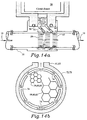
- FIG. 13a shows honeycomb screens 59, 60 and 63 used in a bypass flow microsensor for gases and liquids.
- End view 71 shows an example of a honeycomb design of the screens.
- Honeycomb screen 59 faces flow 16 to calm down turbulence.
- Honeycomb screen 60 then tends to force, by flow restriction and a tortuous path to the sensor inlet, a part of flow 16 with convection up through an offset bypass 61 up to baffle 25 having holes 21.
- the reduced flow makes for a lower influence of turbulence.
- the tortuous path makes it difficult for heavier particles to flow into the volume about baffle 25.
- Baffle 25 is the convection barrier, and diffusion of the fluid occurs in volume 22. Fluid is forced down a bypass channel 62 into pipe 31, and joins flow 16 through another honeycomb screen 63. The driving force of the fluid into and out of bypass channels 61 and 62, respectively, is provided by the pressure drop across screen 60 only.
- Figure 14a shows a configuration like that of figure 13b except it has multiple port (i.e., piezometric) sampling devices 72 and 73, which are channels around the main fluid conveyance mechanism or pipe 31 with a half of a dozen or more ports 74 from pipe 31 to the respective channel around the pipe. From device 72, fluid goes to bypass channel 61, to barrier 25 and returns back into pipe 31 via bypass channel 62, to device 73 and ports 74. Devices 72 and 73 reduce and average the effects of noise and the turbulent effects of flow 16 upon the convection of fluid into the volume about convection barrier 25.
- Figure 14b shows a flow channel cross-section of a multiport piezometric sampling device 72, 73.
- O-ring seals 30 are used to seal the connection of the thermal property sensor to fluid conveyance or pipe 31.
- Table 1 shows aspects of structures 40, 41, 42 and 43. Among these stands out the tradeoff one makes to eliminate the interference by condensation and switching to a membrane 51 structure 41, 42 or 43.
- the second column in Table 1 lists the unamplified thermal conductivity (TC) sensor signals resulting from switching from N 2 to Ar, corresponding to a drop of 30.8% in TC.
- TC thermal conductivity
- the TC mV signals are lower for the micromembrane 51 structures because only one side of their membrane 51 is exposed to the new sample gas, which amounts to an exact factor of two times, as verified with one membrane chip before and after sealing it to its substrate.
- membrane 51 diameter, thickness and the temperature coefficient of resistance of the Pt-film sensing elements 46 also influence these signals accounts for the listed values, which were measured.
- the bottom row in Table 1 for structure 43 represents the results for a standard microbridge sensor except that its etched-out cavity 50 was refilled with epoxy.
- the rationale for doing this was the desire to sense high mass fluxes or velocity flows, as e.g., with liquids.
- manufactured microbridge flow sensor 11 structures 40 saturate at an air velocity near 30 m/s. It has been previously shown that the high limit of this range can be extended by either sensing the heater power as in classical hot-wire anemometry as shown in Figure 3 (with its consequences of shortened low-flow range and reduced stability), or by increasing the thermal conduction of the sensor elements 46. With the ruggedized structure 43 (Table 1), such an approach was checked out.
- sensor 11 structure 40 for top sensitivity applications; sensor 11 structure 42 for sensitive measurements under conditions of high dust load and probability of condensation; and sensor 11 structure 43 for situations where high mass fluxes need to be sensed, regardless of dustload or condensation.
- Sensor 11 structures 40 and 43 offer the additional feature of being inherently immune to overpressures.
- Dust and particulates if allowed to settle on the chip's sensing elements 46, can alter the heat transfer characteristics, the sensitivities of elements 46 and thus the output signal of sensor 11.
- a tool kit of parameter groups are selected or adjusted for the design of sensor 10. They include sensor chip design and performance, and the geometries of the convective transport section, the convective barrier and the diffusion transport section of the sensor package or housing.
- microbridge structure 40 By comparing the performance of microbridge structure 40 versus micromembrane sensor chip structures 41, 42 and 43, one is able to demonstrate rapid sensor recovery after condensation with a sealed micromembrane structure 41, 42 or 43, but at the price of dropping the thermal conductivity sensitivity by a factor of about two times (the sealed side of membrane 51 is not exposed to the sample fluid), and increasing its sensitivity to changes in absolute pressure, as summarized in Table 1.
- the recommended approach to achieve fast and reliable property sensor operation is to combine convective macroscopic transport 13 of sample fluid 14 up to the sensor's microshield 12 or 25, with diffusive transport inside shield 12 or 25 to microsensor 11.
- the package of Figure 4c represents this approach, which performed successfully in our tests.
- sensor 11 is mounted facedown, and is protected from direct line of flight of aerosols from flowing fluid 14 to sensor chip 11.
Description
| RELATIVE SENSITIVITIES OF THERMAL MICROSENSORS TO TC, p AND FLOW | ||||||||||
| Relative Sensitivities | ||||||||||
| Sensor Chip Structure | Th. Cond Signal | ±TC | Abs Press | 2 | Flow Signal* N2 at 7.6 m/s | ±Flow Noise N2 | ||||
| mV | % | mV | rms | mV | %/bar | mV | S/N | mV rms | cms | |
| Commercial µbridge - | -220 | -30.8 | 0.04 | 0.16 | 600 | 120 | 0.33 | |||
| Large µmembrane 41 | -105 | -30.8 | 0.04 | 10.0 | ||||||
| Small, strong µmembrane | -170 | -30.8 | 0.04 | 5.0 | ||||||
| Supported/filled µbridge - | -86 | -30.8 | 0.04 | 0.16 | 150 | 130 | 0.30 | |||
| Before filling | -351 | -30.8 | 0.04 | 0.16 |
Claims (27)
- A housing for a sensor comprising:characterised in that said baffle is a single-stage baffle concentric with said sensor and comprising a first area which overlaps said sensor and which has no opening therein, and a second area which projects around said sensor and which has at least one opening therein.an input;a sensor situated in said housing; anda baffle situated between said input and said sensor,
- The housing of claim 1, wherein said input is a fluid input for location proximate to a fluid conveyance device.
- The housing of claim 2, wherein said baffle is proximate to said sensor.
- The housing of any preceding claim, wherein said baffle has a plurality of openings arranged in said second area projecting around said sensor.
- The housing of any preceding claim, wherein said sensor is a thermal sensor.
- The housing of claim 5, wherein said sensor has a thermal sensing element.
- The housing of claim 6, wherein said input, baffle and sensor are positioned relative to the fluid conveyance device in a direction approximately parallel to a direction of gravity, with the fluid conveyance device closest to earth and said input closer to the fluid conveyance device than said baffle.
- The housing of claim 7, wherein said sensor has a membrane sensing element.
- The housing of claim 8, wherein said sensor has a microbridge sensing element.
- The housing of claim 7, wherein said sensor has a thermal isolating recess proximate to the sensing element.
- The housing of claim 10, wherein the recess is filed with a substance having a low thermal conduction.
- The housing of claim 11, further comprising electronics connected to said sensor.
- The housing of claim 1, wherein
said input port is located at a first end of a structure;
said baffle is attached within said structure and proximate to the input port;
said sensor is attached to said structure and proximate to said shield; and
wherein
said shield and said sensor form a recess between said sensor and said shield. - The housing of claim 13 wherein:said input has a diameter and is situated at a distance from said baffle, anda ratio of the diameter to the distance is close to or greater than one.
- The housing of claim 1, wherein
said sensor is for sensing at least one thermal property of fluid;
said baffle is located, proximate to said sensing means, for shielding said sensing means from convection of the fluid that detrimentally affects an accuracy of the sensing the at least one thermal properly of the fluid; and
said input comprises means for reducing velocity and conveying a portion of fluid to said shield means. - The housing of claim 15, wherein:said baffle is situated more than 50 microns from said sensor means.
- The housing of claim 16, wherein said at least one opening has a diameter and length such that a diameter to length ratio is close to or exceeds one.
- The housing of claim 1, wherein said sensor means comprises:a substrate situated on the surface supporting said sensor means;a semiconductor piece formed on the substrate;the semiconductor has a recess; anda thermal sensing element proximate to the recess.
- The housing of claim 15, wherein:said input comprises a fluid flow bypass channel for bypass fluid conveyance; andthe fluid flow bypass channel is designed such that a first flow velocity of a fluid through the bypass channel is less than a second flow velocity of the fluid of a main fluid conveyance device that said input means is connected to.
- The housing of claim 19, wherein said sensor means is situated in the fluid flow bypass channel.
- The housing of claim 20, wherein:the bypass channel is approximately parallel to the main fluid conveyance device; andfluid flow in and out of the bypass channel has direction changes greater than 90 degrees so that high inertia droplets or particles carried by the fluid have a low probability of following the fluid and thus have a low concentration in the bypass channel.
- The housing of claim 15, wherein:said input has a first end proximate to said baffle and a second end;the second end is an opening that has an area equivalent to a circle having a first diameter;the second end is at a first distance from said baffle; anda ratio of the first diameter to the first distance is close to or greater than one.
- The housing of claim 1, comprising:wherein said baffle is situated between said sensor and the first and second channels; anda first input end having first and second channels;a second end at which said sensor is located;
a first cavity situated between said baffle and the first and second channels; and
a second cavity situated between said baffle and said sensor. - The housing of claim 23, wherein:a fluid flows into said first cavity via the first channel and exits said first cavity via the second channel;said baffle blocks convection flow lines of the fluid from said second cavity;said baffle permits the passage of a diffused fluid into said second cavity; andsaid sensor detects at least one thermal property of the diffused fluid.
- The housing of claim 24, wherein:the first and second channels are connected to a fluid conveyance pipe;the fluid conveyance pipe has at least two screens situated in the fluid conveyance pipe, approximately perpendicular to a flow of a fluid;the screens are placed so as to cause some fluid to enter the first channel and exit the second channel.
- The housing of claim 25, further comprising a piezometric sampling device connected to the fluid conveyance pipe and to the first and second channels.
- The housing of claim 26, wherein:the at least two screens are honeycomb screens; andthe first and second channels are bypass channels.
Applications Claiming Priority (3)
| Application Number | Priority Date | Filing Date | Title |
|---|---|---|---|
| US09/239,125 US6361206B1 (en) | 1999-01-28 | 1999-01-28 | Microsensor housing |
| US239125 | 1999-01-28 | ||
| PCT/US2000/001987 WO2000045163A2 (en) | 1999-01-28 | 2000-01-27 | Microsensor housing |
Publications (2)
| Publication Number | Publication Date |
|---|---|
| EP1149287A1 EP1149287A1 (en) | 2001-10-31 |
| EP1149287B1 true EP1149287B1 (en) | 2003-04-09 |
Family
ID=22900721
Family Applications (1)
| Application Number | Title | Priority Date | Filing Date |
|---|---|---|---|
| EP00908384A Expired - Lifetime EP1149287B1 (en) | 1999-01-28 | 2000-01-27 | Sensor housing |
Country Status (6)
| Country | Link |
|---|---|
| US (1) | US6361206B1 (en) |
| EP (1) | EP1149287B1 (en) |
| JP (1) | JP2002535675A (en) |
| CA (1) | CA2359657C (en) |
| DE (1) | DE60002044T2 (en) |
| WO (1) | WO2000045163A2 (en) |
Families Citing this family (45)
| Publication number | Priority date | Publication date | Assignee | Title |
|---|---|---|---|---|
| US7258003B2 (en) * | 1998-12-07 | 2007-08-21 | Honeywell International Inc. | Flow sensor with self-aligned flow channel |
| US6911894B2 (en) * | 1998-12-07 | 2005-06-28 | Honeywell International Inc. | Sensor package for harsh environments |
| US6322247B1 (en) * | 1999-01-28 | 2001-11-27 | Honeywell International Inc. | Microsensor housing |
| US7168334B1 (en) * | 2000-05-30 | 2007-01-30 | Gambro Lundia Ab | Arrangement for measuring a property of a fluid present in a tube |
| WO2002077613A2 (en) * | 2001-03-23 | 2002-10-03 | Services Petroliers Schlumberger | Fluid property sensors |
| US6838287B2 (en) * | 2001-12-20 | 2005-01-04 | Honeywell International Inc. | Fluid mixture composition sensor |
| US6845664B1 (en) | 2002-10-03 | 2005-01-25 | The United States Of America As Represented By The Administrator Of National Aeronautics And Space Administration | MEMS direct chip attach packaging methodologies and apparatuses for harsh environments |
| DE10314705B3 (en) * | 2003-03-31 | 2004-07-01 | Heraeus Sensor Technology Gmbh | Temperature sensor for flowing medium in pipe or flexible hose has ceramics substrate with thin film resistor held between ends of two metal conductor strips in plastics housing surrounding pipe |
| US7131766B2 (en) * | 2003-07-16 | 2006-11-07 | Delphi Technologies, Inc. | Temperature sensor apparatus and method |
| US7003418B2 (en) * | 2003-08-28 | 2006-02-21 | Honeywell International Inc. | Methods and systems for temperature compensation of physical property sensors |
| US7229669B2 (en) * | 2003-11-13 | 2007-06-12 | Honeywell International Inc. | Thin-film deposition methods and apparatuses |
| US7021821B2 (en) * | 2004-05-28 | 2006-04-04 | Honeywell International Inc. | Differential thermal sensors |
| DE102005007872B3 (en) * | 2005-02-21 | 2006-06-22 | MAX-PLANCK-Gesellschaft zur Förderung der Wissenschaften e.V. | Temperature measurement in microfluidic channel of microfluidic device, comprises irradiating volume element of the channel by pulsed laser, elastic scattering and detecting Raman light and converting the Raman light to signals |
| GB0605683D0 (en) * | 2006-03-21 | 2006-05-03 | Servomex Group Ltd | Thermal conductivity sensor |
| FR2908515B1 (en) * | 2006-11-09 | 2008-12-26 | Actaris Sas Soc Par Actions Si | CELL FOR MEASURING THE THERMAL CONDUCTIVITY OF A GAS |
| US7726876B2 (en) * | 2007-03-14 | 2010-06-01 | Entegris, Inc. | System and method for non-intrusive thermal monitor |
| US20080250854A1 (en) * | 2007-04-12 | 2008-10-16 | Junhua Ding | Mass flow device using a flow equalizer for improving the output response |
| GB0720905D0 (en) * | 2007-10-25 | 2007-12-05 | Cambridge Entpr Ltd | Shear stress sensors |
| DE102008029793A1 (en) * | 2008-03-19 | 2009-10-01 | Epcos Ag | measuring device |
| US7748268B2 (en) * | 2008-07-13 | 2010-07-06 | Brooks Instrument, Llc | Thermal flow meter |
| DE102009056331B4 (en) * | 2009-12-01 | 2014-10-16 | Continental Automotive Gmbh | Hydrogen sensor and detection method of a hydrogen concentration |
| EP2606318B1 (en) * | 2010-08-17 | 2017-03-22 | Sensirion AG | Flow sensor arrangement |
| EP2527799B1 (en) * | 2011-05-25 | 2020-03-18 | Sensirion AG | Flow sensor arrangement |
| EP2645091B1 (en) | 2012-03-30 | 2018-10-17 | ams international AG | Integrated circuit comprising a gas sensor |
| DE102013101203A1 (en) * | 2013-02-07 | 2014-08-07 | Sick Ag | sensor |
| US9618653B2 (en) * | 2013-03-29 | 2017-04-11 | Stmicroelectronics Pte Ltd. | Microelectronic environmental sensing module |
| US9176089B2 (en) | 2013-03-29 | 2015-11-03 | Stmicroelectronics Pte Ltd. | Integrated multi-sensor module |
| JP6099094B2 (en) * | 2013-06-21 | 2017-03-22 | 日立オートモティブシステムズ株式会社 | Gas sensor device and gas sensor device mounting structure |
| DE102013015218A1 (en) | 2013-09-13 | 2015-03-19 | Hella Kgaa Hueck & Co. | Gas sensor and motor vehicle with a gas sensor |
| US9976409B2 (en) | 2013-10-08 | 2018-05-22 | Halliburton Energy Services, Inc. | Assembly for measuring temperature of materials flowing through tubing in a well system |
| WO2015053749A1 (en) * | 2013-10-08 | 2015-04-16 | Halliburton Energy Services, Inc. | Assembly for measuring temperature of materials flowing through tubing in a well system |
| US9770196B2 (en) * | 2013-11-27 | 2017-09-26 | Universiteit Gent | Sensing of components in liquids |
| GB201421102D0 (en) * | 2014-11-27 | 2015-01-14 | Cambridge Entpr Ltd | Thermal conductivity sensing device, methods for operation and uses of the same |
| US9945800B2 (en) * | 2015-07-23 | 2018-04-17 | Caterpillar Inc. | Fuel gas composition sensing system |
| US10775341B2 (en) * | 2016-03-25 | 2020-09-15 | Ngk Insulators, Ltd. | Sensor element, manufacturing method therefor, and gas sensor |
| JP6739525B2 (en) * | 2016-05-23 | 2020-08-12 | 日立オートモティブシステムズ株式会社 | Humidity measuring device |
| US10429330B2 (en) | 2016-07-18 | 2019-10-01 | Stmicroelectronics Pte Ltd | Gas analyzer that detects gases, humidity, and temperature |
| US10254261B2 (en) | 2016-07-18 | 2019-04-09 | Stmicroelectronics Pte Ltd | Integrated air quality sensor that detects multiple gas species |
| US10557812B2 (en) | 2016-12-01 | 2020-02-11 | Stmicroelectronics Pte Ltd | Gas sensors |
| DE102018200171B4 (en) * | 2018-01-08 | 2020-04-02 | Audi Ag | Measuring arrangement for determining a parameter of a fluid medium flowing through a fluid flow channel, and fluid flow channel with such a measuring arrangement |
| EP3899445A1 (en) * | 2018-12-20 | 2021-10-27 | Edwards Lifesciences Corporation | Thermal mass fluid flow sensor |
| US10982985B2 (en) * | 2019-03-04 | 2021-04-20 | Hitachi Metals, Ltd. | High flow tubular bypass |
| US11280651B2 (en) * | 2019-03-25 | 2022-03-22 | Flo Technologies, Inc. | Thin film thermal mass flow sensor in fluid applications |
| EP4184159A4 (en) * | 2020-07-16 | 2023-12-27 | Panasonic Intellectual Property Management Co., Ltd. | Physical quantity measurement device |
| DE102021212418A1 (en) * | 2021-11-04 | 2023-05-04 | Robert Bosch Gesellschaft mit beschränkter Haftung | Sensor for detecting at least one property of a fluid medium in a measuring room |
Family Cites Families (26)
| Publication number | Priority date | Publication date | Assignee | Title |
|---|---|---|---|---|
| US2496806A (en) * | 1946-11-27 | 1950-02-07 | United Aircraft Corp | Gas temperature probe of the thermocouple type |
| US2928279A (en) * | 1955-09-01 | 1960-03-15 | North American Aviation Inc | Stagnation air temperature measuring device |
| US3675489A (en) | 1970-09-18 | 1972-07-11 | Montedison Spa | Apparatus for the drawing of samples of gaseous mixtures to be analyzed |
| US3720093A (en) | 1970-12-03 | 1973-03-13 | Us Navy | Carbon dioxide indicating meter |
| US3881181A (en) * | 1973-02-22 | 1975-04-29 | Rca Corp | Semiconductor temperature sensor |
| US4488414A (en) | 1983-10-03 | 1984-12-18 | Honeywell Inc. | Disc detector assembly |
| JPS60128318A (en) * | 1983-12-16 | 1985-07-09 | Mitsubishi Heavy Ind Ltd | Gas temperature measuring device |
| US4682503A (en) | 1986-05-16 | 1987-07-28 | Honeywell Inc. | Microscopic size, thermal conductivity type, air or gas absolute pressure sensor |
| US4914742A (en) * | 1987-12-07 | 1990-04-03 | Honeywell Inc. | Thin film orthogonal microsensor for air flow and method |
| JPH0643907B2 (en) * | 1988-12-15 | 1994-06-08 | 山武ハネウエル株式会社 | Flowmeter |
| AU6409490A (en) | 1989-09-23 | 1991-04-18 | University Court Of The University Of Dundee, The | A method of and apparatus for monitoring gas |
| US5060514A (en) * | 1989-11-30 | 1991-10-29 | Puritan-Bennett Corporate | Ultrasonic gas measuring device |
| US5177696A (en) * | 1989-12-28 | 1993-01-05 | Honeywell Inc. | Method of determination of gas properties at reference conditions |
| US5081866A (en) * | 1990-05-30 | 1992-01-21 | Yamatake-Honeywell Co., Ltd. | Respiratory air flowmeter |
| US5056362A (en) * | 1990-07-25 | 1991-10-15 | Siemens Automotive L.P. | Strengthening a silicon micromachined mass air flow sensor in the region of its hot element |
| US5303167A (en) * | 1991-03-08 | 1994-04-12 | Honeywell Inc. | Absolute pressure sensor and method |
| US5220830A (en) * | 1991-07-09 | 1993-06-22 | Honeywell Inc. | Compact gas flow meter using electronic microsensors |
| US5249462A (en) * | 1991-07-09 | 1993-10-05 | Honeywell Inc. | Safe channel design for flow sensor chip microbridges |
| DE4218379C2 (en) | 1992-06-04 | 1995-04-13 | Dirk Tillich | Device for the separation of suspended matter in flowing liquids |
| US5279155A (en) * | 1993-02-04 | 1994-01-18 | Honeywell, Inc. | Mass airflow sensor |
| IL109388A0 (en) * | 1993-04-29 | 1994-07-31 | Rosemount Aerospace Inc | Temperature sensor with integral debris guard |
| DE4324659C1 (en) | 1993-07-22 | 1995-04-06 | Siemens Ag | Sensor with a sensor element arranged in a housing |
| US5653538A (en) * | 1995-06-07 | 1997-08-05 | Rosemount Aerospace Inc. | Total temperature probe |
| EP0882978A1 (en) | 1997-06-04 | 1998-12-09 | STMicroelectronics S.r.l. | Integrated semi-conductor device comprising a chemoresistive gas microsensor and manufacturing process thereof |
| US6184773B1 (en) * | 1998-12-07 | 2001-02-06 | Honeywell Inc. | Rugged fluid flow and property microsensor |
| US6178811B1 (en) * | 1999-03-11 | 2001-01-30 | Honeywell International Inc. | Quasi-static viscometer |
-
1999
- 1999-01-28 US US09/239,125 patent/US6361206B1/en not_active Expired - Lifetime
-
2000
- 2000-01-27 EP EP00908384A patent/EP1149287B1/en not_active Expired - Lifetime
- 2000-01-27 JP JP2000596365A patent/JP2002535675A/en active Pending
- 2000-01-27 CA CA002359657A patent/CA2359657C/en not_active Expired - Fee Related
- 2000-01-27 WO PCT/US2000/001987 patent/WO2000045163A2/en active IP Right Grant
- 2000-01-27 DE DE60002044T patent/DE60002044T2/en not_active Expired - Lifetime
Also Published As
| Publication number | Publication date |
|---|---|
| WO2000045163A3 (en) | 2000-12-14 |
| EP1149287A1 (en) | 2001-10-31 |
| CA2359657C (en) | 2008-12-02 |
| DE60002044T2 (en) | 2003-12-04 |
| WO2000045163A2 (en) | 2000-08-03 |
| JP2002535675A (en) | 2002-10-22 |
| DE60002044D1 (en) | 2003-05-15 |
| US6361206B1 (en) | 2002-03-26 |
| CA2359657A1 (en) | 2000-08-03 |
Similar Documents
| Publication | Publication Date | Title |
|---|---|---|
| EP1149287B1 (en) | Sensor housing | |
| US6322247B1 (en) | Microsensor housing | |
| US5220830A (en) | Compact gas flow meter using electronic microsensors | |
| Johnson et al. | A highly sensitive silicon chip microtransducer for air flow and differential pressure sensing applications | |
| EP2482043B1 (en) | Flow sensor assembly with integral bypass channel | |
| US7614295B2 (en) | Flow sensor | |
| US7878047B2 (en) | Monitoring particles in a fluid stream | |
| US7021821B2 (en) | Differential thermal sensors | |
| US7490512B2 (en) | Detector of low levels of gas pressure and flow | |
| US4461173A (en) | Multirange flowmeter | |
| US4787251A (en) | Directional low differential pressure transducer | |
| EP0305134B1 (en) | Fluid metering system | |
| US4856328A (en) | Sampling probe flow sensor | |
| JPH01206218A (en) | Flowmeter | |
| US8065925B2 (en) | Sensor unit having a measuring probe and a housing part with sensors and a computing unit integrated in the housing part | |
| EP0079942B1 (en) | Flow splitting device for fluid flow meter | |
| US3785206A (en) | Fluid flow measuring device | |
| US5347876A (en) | Gas flowmeter using thermal time-of-flight principle | |
| EP1943494B1 (en) | Monitoring particles in a fluid stream | |
| JP6247499B2 (en) | Gas flow meter | |
| JPH0324973B2 (en) | ||
| JP3272797B2 (en) | Area flow meter | |
| JPH06258106A (en) | Differential pressure flowrate meter | |
| KR20060015730A (en) | Thermal anemometry mass flow measurement apparatus and method | |
| JPH05142002A (en) | Fluidic gas meter |
Legal Events
| Date | Code | Title | Description |
|---|---|---|---|
| PUAI | Public reference made under article 153(3) epc to a published international application that has entered the european phase |
Free format text: ORIGINAL CODE: 0009012 |
|
| 17P | Request for examination filed |
Effective date: 20010726 |
|
| AK | Designated contracting states |
Kind code of ref document: A1 Designated state(s): AT BE CH CY DE DK ES FI FR GB GR IE IT LI LU MC NL PT SE Kind code of ref document: A1 Designated state(s): BE DE FR GB NL |
|
| 17Q | First examination report despatched |
Effective date: 20020118 |
|
| RTI1 | Title (correction) |
Free format text: SENSOR HOUSING |
|
| RTI1 | Title (correction) |
Free format text: SENSOR HOUSING |
|
| GRAH | Despatch of communication of intention to grant a patent |
Free format text: ORIGINAL CODE: EPIDOS IGRA |
|
| GRAH | Despatch of communication of intention to grant a patent |
Free format text: ORIGINAL CODE: EPIDOS IGRA |
|
| GRAA | (expected) grant |
Free format text: ORIGINAL CODE: 0009210 |
|
| AK | Designated contracting states |
Designated state(s): BE DE FR GB NL |
|
| REG | Reference to a national code |
Ref country code: GB Ref legal event code: FG4D |
|
| REG | Reference to a national code |
Ref country code: IE Ref legal event code: FG4D |
|
| ET | Fr: translation filed | ||
| PLBE | No opposition filed within time limit |
Free format text: ORIGINAL CODE: 0009261 |
|
| STAA | Information on the status of an ep patent application or granted ep patent |
Free format text: STATUS: NO OPPOSITION FILED WITHIN TIME LIMIT |
|
| 26N | No opposition filed |
Effective date: 20040112 |
|
| REG | Reference to a national code |
Ref country code: IE Ref legal event code: MM4A |
|
| PGFP | Annual fee paid to national office [announced via postgrant information from national office to epo] |
Ref country code: NL Payment date: 20071219 Year of fee payment: 9 |
|
| PGFP | Annual fee paid to national office [announced via postgrant information from national office to epo] |
Ref country code: BE Payment date: 20080201 Year of fee payment: 9 |
|
| NLV4 | Nl: lapsed or anulled due to non-payment of the annual fee |
Effective date: 20090801 |
|
| PG25 | Lapsed in a contracting state [announced via postgrant information from national office to epo] |
Ref country code: NL Free format text: LAPSE BECAUSE OF NON-PAYMENT OF DUE FEES Effective date: 20090801 |
|
| PG25 | Lapsed in a contracting state [announced via postgrant information from national office to epo] |
Ref country code: BE Free format text: LAPSE BECAUSE OF NON-PAYMENT OF DUE FEES Effective date: 20090131 |
|
| REG | Reference to a national code |
Ref country code: FR Ref legal event code: PLFP Year of fee payment: 17 |
|
| REG | Reference to a national code |
Ref country code: FR Ref legal event code: PLFP Year of fee payment: 18 |
|
| REG | Reference to a national code |
Ref country code: FR Ref legal event code: PLFP Year of fee payment: 19 |
|
| PGFP | Annual fee paid to national office [announced via postgrant information from national office to epo] |
Ref country code: GB Payment date: 20190130 Year of fee payment: 20 Ref country code: FR Payment date: 20190128 Year of fee payment: 20 |
|
| PGFP | Annual fee paid to national office [announced via postgrant information from national office to epo] |
Ref country code: DE Payment date: 20190401 Year of fee payment: 20 |
|
| REG | Reference to a national code |
Ref country code: DE Ref legal event code: R071 Ref document number: 60002044 Country of ref document: DE |
|
| REG | Reference to a national code |
Ref country code: GB Ref legal event code: PE20 Expiry date: 20200126 |
|
| PG25 | Lapsed in a contracting state [announced via postgrant information from national office to epo] |
Ref country code: GB Free format text: LAPSE BECAUSE OF EXPIRATION OF PROTECTION Effective date: 20200126 |
|
| P01 | Opt-out of the competence of the unified patent court (upc) registered |
Effective date: 20230523 |