EP1148774A1 - Emi shielding for portable electronic devices - Google Patents
Emi shielding for portable electronic devices Download PDFInfo
- Publication number
- EP1148774A1 EP1148774A1 EP01301254A EP01301254A EP1148774A1 EP 1148774 A1 EP1148774 A1 EP 1148774A1 EP 01301254 A EP01301254 A EP 01301254A EP 01301254 A EP01301254 A EP 01301254A EP 1148774 A1 EP1148774 A1 EP 1148774A1
- Authority
- EP
- European Patent Office
- Prior art keywords
- fiber mesh
- mesh net
- emi shielding
- further characterized
- set forth
- Prior art date
- Legal status (The legal status is an assumption and is not a legal conclusion. Google has not performed a legal analysis and makes no representation as to the accuracy of the status listed.)
- Ceased
Links
- 239000000835 fiber Substances 0.000 claims abstract description 156
- 230000001413 cellular effect Effects 0.000 claims abstract description 10
- 229920006254 polymer film Polymers 0.000 claims description 17
- 238000000034 method Methods 0.000 claims description 12
- 238000000465 moulding Methods 0.000 claims description 7
- 239000000758 substrate Substances 0.000 claims description 4
- 239000004753 textile Substances 0.000 claims description 4
- 239000000203 mixture Substances 0.000 claims description 3
- 230000008878 coupling Effects 0.000 claims description 2
- 238000010168 coupling process Methods 0.000 claims description 2
- 238000005859 coupling reaction Methods 0.000 claims description 2
- 239000002991 molded plastic Substances 0.000 claims 1
- 229920000642 polymer Polymers 0.000 abstract description 2
- 229910052751 metal Inorganic materials 0.000 description 11
- 239000002184 metal Substances 0.000 description 11
- -1 polypropylenes Polymers 0.000 description 8
- 230000013011 mating Effects 0.000 description 7
- 239000004743 Polypropylene Substances 0.000 description 6
- 230000002093 peripheral effect Effects 0.000 description 6
- PXHVJJICTQNCMI-UHFFFAOYSA-N Nickel Chemical compound [Ni] PXHVJJICTQNCMI-UHFFFAOYSA-N 0.000 description 4
- 239000004952 Polyamide Substances 0.000 description 4
- 239000011248 coating agent Substances 0.000 description 4
- 238000000576 coating method Methods 0.000 description 4
- 239000004020 conductor Substances 0.000 description 4
- 229920002647 polyamide Polymers 0.000 description 4
- 229920001155 polypropylene Polymers 0.000 description 4
- BQCADISMDOOEFD-UHFFFAOYSA-N Silver Chemical group [Ag] BQCADISMDOOEFD-UHFFFAOYSA-N 0.000 description 3
- 239000000463 material Substances 0.000 description 3
- 238000005259 measurement Methods 0.000 description 3
- 229920000728 polyester Polymers 0.000 description 3
- 230000005855 radiation Effects 0.000 description 3
- 229910052709 silver Inorganic materials 0.000 description 3
- 239000004332 silver Substances 0.000 description 3
- 238000012360 testing method Methods 0.000 description 3
- 238000005303 weighing Methods 0.000 description 3
- 229920003043 Cellulose fiber Polymers 0.000 description 2
- RYGMFSIKBFXOCR-UHFFFAOYSA-N Copper Chemical compound [Cu] RYGMFSIKBFXOCR-UHFFFAOYSA-N 0.000 description 2
- 229920000742 Cotton Polymers 0.000 description 2
- 229920001410 Microfiber Polymers 0.000 description 2
- 239000004698 Polyethylene Substances 0.000 description 2
- 229910052782 aluminium Inorganic materials 0.000 description 2
- XAGFODPZIPBFFR-UHFFFAOYSA-N aluminium Chemical compound [Al] XAGFODPZIPBFFR-UHFFFAOYSA-N 0.000 description 2
- 230000008901 benefit Effects 0.000 description 2
- 239000000919 ceramic Substances 0.000 description 2
- 239000010949 copper Substances 0.000 description 2
- 229910052802 copper Inorganic materials 0.000 description 2
- 239000002657 fibrous material Substances 0.000 description 2
- 239000011521 glass Substances 0.000 description 2
- 238000009940 knitting Methods 0.000 description 2
- 239000003658 microfiber Substances 0.000 description 2
- 229910052759 nickel Inorganic materials 0.000 description 2
- 229920000573 polyethylene Polymers 0.000 description 2
- 229920000139 polyethylene terephthalate Polymers 0.000 description 2
- 239000005020 polyethylene terephthalate Substances 0.000 description 2
- 102000004169 proteins and genes Human genes 0.000 description 2
- 108090000623 proteins and genes Proteins 0.000 description 2
- 230000003252 repetitive effect Effects 0.000 description 2
- 229920002302 Nylon 6,6 Polymers 0.000 description 1
- 239000002253 acid Substances 0.000 description 1
- 150000007513 acids Chemical class 0.000 description 1
- 239000000956 alloy Substances 0.000 description 1
- 229910045601 alloy Inorganic materials 0.000 description 1
- 230000004888 barrier function Effects 0.000 description 1
- UQMRAFJOBWOFNS-UHFFFAOYSA-N butyl 2-(2,4-dichlorophenoxy)acetate Chemical compound CCCCOC(=O)COC1=CC=C(Cl)C=C1Cl UQMRAFJOBWOFNS-UHFFFAOYSA-N 0.000 description 1
- 230000001419 dependent effect Effects 0.000 description 1
- 150000002009 diols Chemical class 0.000 description 1
- 230000000694 effects Effects 0.000 description 1
- 230000005670 electromagnetic radiation Effects 0.000 description 1
- 239000004744 fabric Substances 0.000 description 1
- 239000000976 ink Substances 0.000 description 1
- 238000003780 insertion Methods 0.000 description 1
- 230000037431 insertion Effects 0.000 description 1
- 239000003562 lightweight material Substances 0.000 description 1
- 238000004519 manufacturing process Methods 0.000 description 1
- 238000012986 modification Methods 0.000 description 1
- 230000004048 modification Effects 0.000 description 1
- 239000012811 non-conductive material Substances 0.000 description 1
- 239000004033 plastic Substances 0.000 description 1
- 229920003023 plastic Polymers 0.000 description 1
- 230000008569 process Effects 0.000 description 1
- 238000001228 spectrum Methods 0.000 description 1
- 239000007921 spray Substances 0.000 description 1
- 230000001052 transient effect Effects 0.000 description 1
- 238000003466 welding Methods 0.000 description 1
Images


Classifications
-
- H—ELECTRICITY
- H05—ELECTRIC TECHNIQUES NOT OTHERWISE PROVIDED FOR
- H05K—PRINTED CIRCUITS; CASINGS OR CONSTRUCTIONAL DETAILS OF ELECTRIC APPARATUS; MANUFACTURE OF ASSEMBLAGES OF ELECTRICAL COMPONENTS
- H05K9/00—Screening of apparatus or components against electric or magnetic fields
- H05K9/0073—Shielding materials
- H05K9/0081—Electromagnetic shielding materials, e.g. EMI, RFI shielding
- H05K9/009—Electromagnetic shielding materials, e.g. EMI, RFI shielding comprising electro-conductive fibres, e.g. metal fibres, carbon fibres, metallised textile fibres, electro-conductive mesh, woven, non-woven mat, fleece, cross-linked
-
- D—TEXTILES; PAPER
- D04—BRAIDING; LACE-MAKING; KNITTING; TRIMMINGS; NON-WOVEN FABRICS
- D04C—BRAIDING OR MANUFACTURE OF LACE, INCLUDING BOBBIN-NET OR CARBONISED LACE; BRAIDING MACHINES; BRAID; LACE
- D04C1/00—Braid or lace, e.g. pillow-lace; Processes for the manufacture thereof
- D04C1/06—Braid or lace serving particular purposes
-
- D—TEXTILES; PAPER
- D04—BRAIDING; LACE-MAKING; KNITTING; TRIMMINGS; NON-WOVEN FABRICS
- D04C—BRAIDING OR MANUFACTURE OF LACE, INCLUDING BOBBIN-NET OR CARBONISED LACE; BRAIDING MACHINES; BRAID; LACE
- D04C1/00—Braid or lace, e.g. pillow-lace; Processes for the manufacture thereof
- D04C1/06—Braid or lace serving particular purposes
- D04C1/08—Tulle fabrics
-
- H—ELECTRICITY
- H05—ELECTRIC TECHNIQUES NOT OTHERWISE PROVIDED FOR
- H05K—PRINTED CIRCUITS; CASINGS OR CONSTRUCTIONAL DETAILS OF ELECTRIC APPARATUS; MANUFACTURE OF ASSEMBLAGES OF ELECTRICAL COMPONENTS
- H05K9/00—Screening of apparatus or components against electric or magnetic fields
- H05K9/0007—Casings
- H05K9/002—Casings with localised screening
- H05K9/0022—Casings with localised screening of components mounted on printed circuit boards [PCB]
- H05K9/0024—Shield cases mounted on a PCB, e.g. cans or caps or conformal shields
- H05K9/003—Shield cases mounted on a PCB, e.g. cans or caps or conformal shields made from non-conductive materials comprising an electro-conductive coating
-
- D—TEXTILES; PAPER
- D10—INDEXING SCHEME ASSOCIATED WITH SUBLASSES OF SECTION D, RELATING TO TEXTILES
- D10B—INDEXING SCHEME ASSOCIATED WITH SUBLASSES OF SECTION D, RELATING TO TEXTILES
- D10B2401/00—Physical properties
- D10B2401/16—Physical properties antistatic; conductive
Definitions
- the present invention relates broadly to electromagnetic interference (EMI) shielding and more specifically, but not exclusively, relates to EMI shielding for portable electronic devices such as cellular or radio telephones.
- EMI electromagnetic interference
- Such electromagnetic signals often develop as a field or as a transient within the radio frequency band of the electromagnetic spectrum, i.e., from between about 10 KHz and 10 GHz, and is termed electromagnetic interference or EMI as being known to interfere with the proper operation of the electronic circuitry of other proximate electronic devices.
- Cellular or radio telephones in particular are required by law to adhere to Electromagnetic Compatibility (EMC) limits as laid down in Type Approval Specifications for Mobile Phones.
- EMC Electromagnetic Compatibility
- shielding having the capability of absorbing and/or reflecting EMI energy may be employed both to confine the EMI energy within a source device, and to insulate the device or other target devices from other source devices.
- Such shielding is provided as a barrier which is inserted between the source and the other devices, and is typically configured as an electrically conductive and grounded housing which encloses the device.
- housings are provided with openable or removable accesses such as doors, hatches, panels, or covers.
- there are gaps between the accesses and the corresponding mating surfaces which reduce the efficiency of the shielding by presenting openings through which electromagnetic energy may leak or otherwise pass into or out of the device.
- gaps represent discontinuities in the surface and ground conductivity of the housing or other shielding, and may even generate a secondary source of EMI radiation by functioning as a form of slot antenna. Any bulk or surface currents induced within the device housing develop voltage gradients across any interface gaps in the shielding thereby causing the gaps to function as antennae which radiate EMI noise.
- One preferred shielding solution is to use a cover or housing shell made of metal to absorb and shield any EMI radiation energy generated by the electronic device.
- One drawback of such metal covers is additional weight and cost which is added to the electronic device.
- a further drawback is the inability and difficulty to form the metal sheet to a desired shape and contour of the electronic device housing thereby requiring the electronic device to be larger and less aesthetically pleasing than would otherwise be possible if not for the metal enclosure required for the EMI shielding.
- One proposed solution to reduce the weight and accommodate the shape and contour of the electronic device is to spray a metallized surface coating on the interior of a lightweight plastic or other suitable lightweight material forming the electronic device housing. Although this has the advantage of reducing the weight, the cost is increased due to the additional step of applying the metallized coating which complicates the manufacturing process and the cost of the metallic coating itself. Additionally, the metallized coating is easily scratched which reduces its shielding effectiveness.
- a further problem is that the mating surface of the electronic device housing covers regardless of the material is not perfectly flat so that mating interfaces provide gaps from which EMI radiation energy can escape.
- Gaskets and other seals have been proposed for filling the gaps within mating surfaces of housings and other EMI shielding structures while maintaining electrical continuity across the structure.
- Such gaskets or seals are bonded or mechanically attached to or pressfitted into one of the mating surfaces and function to close any interface gap to establish a continuous conductive path thereacross by conforming under an applied pressure to irregularities between the surfaces.
- even pressure on the gasket interfaces may also generate gaps between the gasket surface and the ground layer and function as slot antenna to radiate EMI noise.
- gaskets are also subject to shielding failures due to problems with compressibility, resiliency, and attachment. Further, there is an increasing demand in new products to make them smaller by reducing the number of screws, fastening devices and contact points which will require a more efficient and cost effective method for EMI shielding to accommodate these demands.
- an EMI shielding solution for a portable electronic device includes an electrically conductive fiber mesh net insert molded into the walls defining an interior cavity of the device to surround and shield first electronic circuitry contained within the device.
- At least a portion of the fiber mesh net is brought into direct continuous physical and electrical contact with a ground plane carried on a circuit board substrate within the electronic device.
- an EMI shielding solution for a portable electronic device includes an electrically conductive fiber mesh net laminated to a surface of a polymer film sheet.
- the polymer film sheet has an electrically non-conductive surface opposite the fiber mesh net surface for carrying second electronic circuitry, and at least a portion of the fiber mesh net extends to the non-conductive side for mechanical and electrical coupling to the second electronic circuitry.
- the fiber mesh net is a mixture of conductive and non-conductive fibers with at least one of the conductive fibers carrying electrical signals from the first electronic circuitry on the printed circuit board to the second electronic circuitry.
- the fiber mesh consists of natural fibers or filaments such as cotton and other cellulose fibers, silk or other protein fibers and/or glass or other ceramic fibers.
- the fiber mesh consists of man-made synthetic, regenerated or metal fiber and filaments, such as polyesters, polyamides, polypropylenes, polyethylenes and cellulosics, and particularly suited are PES, PA6.6, PA6, PP and copper.
- Fibers, filaments, and yarns can be coated by a thin layer of a conductive metal layer thickness of 10-10000nm, and preferably the conductive metal layer is a silver, nickel or aluminum layer.
- the fiber fineness can be varied from 0.05 den (0.055 dtex) microfiber to 100 den (110 dtex) monofilament whereas the yarn fineness can be extended according to the mesh type up to 300 den (33 tex) .
- the fiber mesh net consists of a bobbinet woven 3-directional net having 6 to 34 openings per inch and a specific weight of 10 to 50 grams per square meter.
- the fiber mesh consists of warp knitted, woven, Raschel, braided nonwoven or spun multidirectional nets, respectively.
- a fiber mesh net of the type contemplated by the present invention is shown therein and designated generally at 10.
- the fiber mesh net 10 is typically made up of a number of electrically conductive fibers or strands 12, 12 which are intertwisted to form threads 14, 14.
- the threads 14, 14 are woven or knit in a repetitive pattern to form a sheetlike structure such as the one shown in Fig. 1.
- a further magnified view of a section of a fiber mesh net of the type which may be practiced with the present invention is shown in Fig. 4 and designated generally at 20.
- a magnified view of a section of the fiber mesh net 20 is shown in Fig. 5. As can be seen in Fig.
- Fig. 6 illustrates a yet further example of a fiber mesh net of the type which may be practiced in the present invention and is designated generally at 30.
- a magnified view of a section of the fiber mesh net 30 illustrated in Fig. 6 and shown in Fig. 7 shows the pattern of woven threads of the fiber mesh net 30.
- the fiber mesh net 30 illustrated in Fig. 6 and its corresponding magnified pattern illustrated in Fig. 7 differ from the fiber mesh nets 10, 20 illustrated in Figs.
- a bobbinet is defined as a set of hexagonal mesh and as can be seen from the magnified views of Figs. 2, 5 and 7, the repetitive patterns are six-sided with each side being designated generally a, b, c, d, e, f, respectively as shown therein.
- Each of the respective patterns define an opening designated generally at 11, 21, 31 in Figs. 2, 5 and 7, respectively.
- the fiber mesh net is a bobbinet woven 3-directional net having 6 to 34 openings per inch and a specific weight of 10 to 50 grams per square meter.
- the fiber mesh nets 10, 20, 30 are preferably a bobbinet woven fiber mesh net
- other textile structures such as warp knitted, woven, Raschel, braided, nonwoven or spun multidirectional structures providing the desired electrically conductive EMI shielding characteristics are also useable to provide the EMI shielding structure of the present invention.
- Raschel is characterized by warp knitting with needle bars, latch needles and removal and holding cams as known by those skilled in the art of knitting.
- Fig. 8 illustrates a somewhat schematic edge end view of the fiber mesh nets of Figs. 1, 4 or 6 as showing the terminal ends of the threads 14, 14.
- the threads 14, 14 are shown as multiple intertwisted strands, the threads can be a single strand or fiber.
- the shielding effectiveness of the fiber mesh net of the present invention is dependent upon and related to the fiber material and thickness or diameter of the fiber.
- the fiber material may be natural or synthetic, metal or alloy, conductive or non-conductive, or conductively coated non-conductive material.
- the fiber mesh may be made of natural fibers or filaments such as cotton and other cellulose fibers, silk or other protein fibers and glass or other ceramic fibers.
- the fiber mesh may also be made of man-made synthetic, regenerated or metal fibers and filaments, for example, polyesters, polyamides, polypropylenes, polyethylenes and cellulosics such as PES (poly(ethylene terephthalate) and other polyesters from diols and terephthalic and other acids), PA6.6 [poly(hexamethylene adipamide)], PA6 [poly( ⁇ -caprolatam)], PP (polypropylene or polypropene) and copper.
- Fibers, filaments, and yarns can be coated by a thin conductive metal layer having an approximate thickness of 10 to 10000nm, and preferably the conductive metal layer a silver, nickel or aluminum layer.
- the fiber fineness can be varied from 0.05 den (0.055 dtex) microfibers to 100 den (110 dtex) monofilament whereas the yarn fineness can be extended according to the mesh type up to 300 den (33 tex).
- Den is an abbreviation for denier which is a unit of fineness or linear density for yarn or fiber equal to the fineness of a yarn or fiber weighing one gram for each 9000 meters.
- Dtex is an abbreviation for decitex which is a unit of fineness or linear density for yarn or fiber equal to the fineness of a yarn or fiber weighing one gram for each 10,000 meters.
- Tex is a unit of fineness or linear density for yarn or fiber equal to the fineness of a yarn or fiber weighing one gram for each 1,000 meters.
- Test measurements of the fiber mesh net 10 made of a PET - Ag blend resulted in a shielding effectiveness of 39.7 dBm at 1 GHz.
- Test measurements of the fiber mesh net 20 made of a polyamide PA and silver-coated polyamide (PA - Ag) combination with a weight of 21 grams/meter 2 and 0.1 millimeter diameter resulted in a shielding effectiveness of 34.0 dBm at 1 GHz.
- Test measurements of the fiber mesh net 30 made of a PA and (PA - Ag) combination with a weight of 17 grams/meter 2 and 0.6 millimeter diameter resulted in a shielding effectiveness of 31.1 dBm at 1 GHz.
- FIG. 9 shows a somewhat schematic cutaway profile view of a cover structure or housing shell 40 wherein the fiber mesh net designated generally at 42 is shown insert molded into a predefined interior cavity 44 formed by the wall 46 of the cover and internal walls 48, 50 of the inner side or electronic circuitry facing side 52 of the cover 40.
- the interior cavity 44 is positioned in the cover to enclose the area of the electronic circuitry within the electronic device that is desired to be EMI shielded when the cover is placed on a receiving housing shell or base structure (not shown) of the electronic device.
- Fig. 9 shows a somewhat schematic cutaway profile view of a cover structure or housing shell 40 wherein the fiber mesh net designated generally at 42 is shown insert molded into a predefined interior cavity 44 formed by the wall 46 of the cover and internal walls 48, 50 of the inner side or electronic circuitry facing side 52 of the cover 40.
- the interior cavity 44 is positioned in the cover to enclose the area of the electronic circuitry within the electronic device that is desired to be EMI shielded when the cover is placed on
- the fiber mesh net 42 is insert molded coextensive with the inner surfaces 54, 56, 58 of the walls 48, 46 and 50, respectively defining the interior cavity 44.
- a portion 60, 62 of the peripheral edge ends of the fiber mesh net 42 extend to a lower surface 64, 66 of the walls 48, 50 respectively.
- the fiber mesh net portions 60, 62 are exposed and define a contact surface for mechanical and electrical contact with a ground plane on an electrical printed circuit board (not shown in Fig. 9) to provide the necessary ground voltage potential for effectuating the necessary EMI shielding.
- the fiber mesh net 42 is insert molded along with the cover 40 such that the fiber mesh net 40 is integrated with the inner surfaces 54, 56, 58 defining the interior cavity 44.
- Fig. 10 illustrates conceptually one means for insert molding the fiber mesh net into a cover structure to form the desired EMI shielding solution described in conjunction with Fig. 9.
- a fiber mesh net sheet embodying the invention and generally designated at 70 is positioned above the desired location in the cover structure to be molded by means of a mold designated generally at 72.
- the mold structure 72 is typically a multi-cavity mold and as illustrated, the particular cavity 74 corresponds to the interior cavity in the cover structure with which the fiber mesh net of the present invention will be insert molded to provide the desired EMI shielding.
- the fiber mesh net sheet 70 is insert molded in the direction illustrated by the arrows 76, 76 into the mold cavity 74 and fuses with the material of the cover structure along the inner surfaces of the cover cavity.
- the resulting cover structure is illustrated in Fig. 11 and designated generally at 80.
- the insert molded fiber mesh net designated generally at 82 is shown in the interior cavity 84 of the cover structure 80.
- a portion of the fiber mesh net 82 defining a peripheral edge 86 of the insert molded fiber mesh net 82 is coextensive with and exposed along the surface 88 immediately adjacent to the cavity 84.
- the fiber mesh net surface is illustrated as being exposed or partially exposed within the interior cavity 84, the fiber mesh net 82 can be totally covered by and within the material forming the cover structure 80.
- the depth that the fiber mesh net 82 is inserted into the mold cavity can be controlled as required for the particular designed cover structure.
- FIG. 12 A somewhat schematic profile cutaway view of the cover structure 80 is illustrated in Fig. 12 to show how the cover 80 co-acts with a receiving housing shell or base structure generally designated at 90 of the electronic device.
- the housing shell 90 carries a printed circuit board 92 upon which electronic circuitry components 94, 94 are carried and which components 94, 94 are to be EMI shielded.
- the printed circuit board 92 has a ground plane 96 on the surface 98 facing the cover structure 80.
- a further embodiment of the present invention is illustrated therein wherein the fiber mesh net EMI shielding structure embodying the present invention is illustrated therein and designated generally at 110.
- the fiber mesh net 110 is illustrated in this embodiment as a preformed molded piece to conform to the shape, size and contour of a corresponding interior cavity 112 of a cover structure 116 such as for example, the type used to encase a portable electronic device such as a cellular or radio telephone.
- the fiber mesh net 110 is formed such that it provides an outer peripheral flange or lip 118 having a lower surface 124 which rests on a corresponding peripheral surface region 120 located on the surface 114 surrounding the cavity 112.
- the electrically conductive fibers of the fiber mesh net mold 110 along the peripheral surface 126 are positioned in facing relationship with a printed circuit board ground plane (not shown in Fig. 13) similar to the configuration as illustrated in connection with the explanation of Fig. 12.
- the fiber mesh net mold 110 is maintained within the cavity 112 through surface-to-surface engagement however, preferably through suitable bonding means.
- the fiber mesh net shown in Figs. 1, 4 or 6 may be desirable to join with a polymer film layer to form a laminate such as illustrated in a somewhat schematic edge end view in Fig. 14.
- the polymer film layer designated generally at 130 and the fiber mesh net designated generally at 132 is located on and bonded to the surface 134 of the polymer film layer 130.
- the laminate generally designated at 136 formed by the polymer film layer 130 and the fiber mesh net 132 is such that at least a portion of the fiber mesh net surface is exposed for mechanical and electrical connection to the ground plane on a printed circuit board as explained above and further to provide flexibility and insert molding into an interior cavity defined in a cover structure as disclosed and described above.
- a somewhat schematic profile view shows a fiber mesh net generally designated at 140 laminated to the inner surfaces 142, 144, 146 of the walls 148, 150, 152, respectively defining an interior cavity generally designated at 154.
- the end portions 156, 158 of the fiber mesh net 140 extend around the lower end surface 160, 162 of the wall 148, 150, respectively.
- the end portions 156, 158 contact a ground plane or ground circuit path of a printed circuit board (not illustrated in Fig. 15) to provide the necessary electrical ground potential for proper EMI shielding.
- Electrical circuitry shown schematically at generally designated 164 is carried on a surface 166 opposite the surface 144 upon which surface 144 the fiber mesh net 140 is laminated.
- the fiber mesh net 140 at the end portion 156 extends across the lower end surface 160 into electrical contact with the circuitry 164 at a connection point generally designated at 168.
- the electrical circuitry 164 carried on the surface 166 does not extend completely across the polymer film surface 166 to the end portion 158 of the fiber mesh net 140.
- the electrical ground potential is carried from the printed circuit board ground plane to the electrical circuitry 164 when the cover is in place as described herein above.
- the electrical circuitry can also be used to provide a ground voltage potential connection for additional components located remote from the printed circuit board carried in the housing shell of the electronic device and external to the cover structure.
- Selected strands of the fiber mesh net 140 are electrically coupled to the electrical circuitry 164 carried by the surface 166 of the polymer layer 143.
- the EMI shielding structure 141 of Fig. 15 can be pre-shaped or pre-formed to conform to the contours of the cavity into which the EMI shielding structure is insert molded such as the interior cavity in a cover structure as described above.
- Fig. 16 shows a somewhat schematic cutaway profile view of a cover structure generally designated at 170 and which cover is similar to the cover structure illustrated in Fig. 9.
- a polymer film laminated with a fiber mesh net 140 on one surface 144 and electrical circuitry 164 on its opposite surface as described in connection with Fig. 15 is insert molded into a predefined interior cavity 172 formed by the wall 174 of the cover 170 and inner walls 176, 178 on the interior side 180 of the cover 170.
- the interior cavity 172 is positioned to enclose the area of the electronic circuitry carried on a printed circuit board (not illustrated in Fig. 16) that is desired to be EMI shielded.
- a printed circuit board not illustrated in Fig. 16
- the fiber mesh net 140 is coextensive with the inner surfaces 142, 144, 146 of the walls 174, 176, 178, respectively defining the cavity 172.
- the end portions 156, 158 of the fiber mesh net 140 are left exposed for electrical and mechanical contact with the ground plane on a printed circuit board as explained above in connection with Fig. 12.
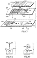
- FIG. 17 a further embodiment of the present invention is illustrated therein as it may be practiced with a portable electronic device such as a cellular or radio telephone.
- a printed circuit board 190 carrying electronic circuitry including components 192, 192 that generate and emit electromagnetic radiation is supported by and carried within a housing shell of the electronic device (not illustrated in Fig. 17).
- the ground voltage potential circuit path or ground plane 194 is carried on the surface 196 of the printed circuit board 190.
- additional electronic circuitry designated generally at 206 is carried on the upward outwardly facing surface 208 and co-acts with an additional laminate overlay generally designated at 210 which may, for example, carry the keys 212, 212 of a dialing pad of the cellular or radio telephone.
- additional electronic circuitry 206 carried on the upper surface 208 of the fiber mesh net and polymer film laminate 202 is accessible to the laminate overlay 210 through an appropriately sized and shaped open portion 214 in the cover 200.
- 17 is to provide a ground voltage potential for a keypad laminate overlay 210
- additional functional circuitry can be carried on the surface 208 and interconnected with other electronic circuitry 216 carried on the printed circuit board 190 to provide additional functions and/or to provide additional mounting area for the functional electronic circuitry of the cellular or radio telephone.
- the techniques for applying printed circuit paths and ground planes using conductive inks and interconnection with electrical circuit components are well known to those skilled in the art of producing electronic circuitry on a flexible circuit substrate.
- Appropriate and desired electronic signals are carried to and from the printed circuit board circuitry components 216 via specific conductive fibers that are pre-identified and fabricated as part of the fiber mesh net of the present invention.
- Certain of the threads, for example thread 32, as illustrated in Fig. 7 may carry an insulated outer jacket over an electrical current carrying center conductor through which the electronic signals may pass back and forth from circuitry 216 on the printed circuit board 190 and circuitry 206 on the laminate surface 208.
- the terminating end of the conductor may be connected to the printed circuit board through various means well known to those skilled in the art for example, as illustrated in Figs. 18 and 19.
- FIG. 18 illustrates a wrapping technique wherein the conductor 220 is wound around a stake or post 222 to make electrical and mechanical connection with the post.
- the post 222 is then inserted into an appropriate mating receiving connector 224 mounted on the printed circuit board 190.
- Fig. 19 shows a conductor end 226 received into an end 228 of a pin 230 and which pin 230 is in turn inserted into an appropriate mating receiving connector 232 mounted on the printed circuit board 190.
- Appropriate miniaturization techniques such as ultrasonic welding can be used to increase the density of connection points from and to fibers of the fiber mesh net.
Landscapes
- Engineering & Computer Science (AREA)
- Microelectronics & Electronic Packaging (AREA)
- Textile Engineering (AREA)
- Manufacturing & Machinery (AREA)
- Physics & Mathematics (AREA)
- Electromagnetism (AREA)
- Shielding Devices Or Components To Electric Or Magnetic Fields (AREA)
- Braiding, Manufacturing Of Bobbin-Net Or Lace, And Manufacturing Of Nets By Knotting (AREA)
- Laminated Bodies (AREA)
- Injection Moulding Of Plastics Or The Like (AREA)
- Knitting Of Fabric (AREA)
Abstract
Description
- The present invention relates broadly to electromagnetic interference (EMI) shielding and more specifically, but not exclusively, relates to EMI shielding for portable electronic devices such as cellular or radio telephones.
- The normal operation of electronic equipment such as computers, communications equipment, portable electronic devices such as cellular or radio telephones, and the like is attended by the generation of electromagnetic signals within the electronic circuitry of the equipment.
- Such electromagnetic signals often develop as a field or as a transient within the radio frequency band of the electromagnetic spectrum, i.e., from between about 10 KHz and 10 GHz, and is termed electromagnetic interference or EMI as being known to interfere with the proper operation of the electronic circuitry of other proximate electronic devices. Cellular or radio telephones in particular are required by law to adhere to Electromagnetic Compatibility (EMC) limits as laid down in Type Approval Specifications for Mobile Phones. "EMC" is defined as the ability of a device to function properly in its intended electromagnetic environment and not to be a source of electromagnetic pollution to that environment.
- To reduce or attenuate the effects of EMI, shielding having the capability of absorbing and/or reflecting EMI energy may be employed both to confine the EMI energy within a source device, and to insulate the device or other target devices from other source devices. Such shielding is provided as a barrier which is inserted between the source and the other devices, and is typically configured as an electrically conductive and grounded housing which encloses the device. As the device generally must remain accessible for servicing or the like, most housings are provided with openable or removable accesses such as doors, hatches, panels, or covers. Typically, there are gaps between the accesses and the corresponding mating surfaces which reduce the efficiency of the shielding by presenting openings through which electromagnetic energy may leak or otherwise pass into or out of the device. Furthermore, such gaps represent discontinuities in the surface and ground conductivity of the housing or other shielding, and may even generate a secondary source of EMI radiation by functioning as a form of slot antenna. Any bulk or surface currents induced within the device housing develop voltage gradients across any interface gaps in the shielding thereby causing the gaps to function as antennae which radiate EMI noise.
- One preferred shielding solution is to use a cover or housing shell made of metal to absorb and shield any EMI radiation energy generated by the electronic device. One drawback of such metal covers is additional weight and cost which is added to the electronic device. A further drawback is the inability and difficulty to form the metal sheet to a desired shape and contour of the electronic device housing thereby requiring the electronic device to be larger and less aesthetically pleasing than would otherwise be possible if not for the metal enclosure required for the EMI shielding. One proposed solution to reduce the weight and accommodate the shape and contour of the electronic device is to spray a metallized surface coating on the interior of a lightweight plastic or other suitable lightweight material forming the electronic device housing. Although this has the advantage of reducing the weight, the cost is increased due to the additional step of applying the metallized coating which complicates the manufacturing process and the cost of the metallic coating itself. Additionally, the metallized coating is easily scratched which reduces its shielding effectiveness.
- A further problem is that the mating surface of the electronic device housing covers regardless of the material is not perfectly flat so that mating interfaces provide gaps from which EMI radiation energy can escape. Gaskets and other seals have been proposed for filling the gaps within mating surfaces of housings and other EMI shielding structures while maintaining electrical continuity across the structure. Such gaskets or seals are bonded or mechanically attached to or pressfitted into one of the mating surfaces and function to close any interface gap to establish a continuous conductive path thereacross by conforming under an applied pressure to irregularities between the surfaces. However, even pressure on the gasket interfaces may also generate gaps between the gasket surface and the ground layer and function as slot antenna to radiate EMI noise. In addition, the gaskets are also subject to shielding failures due to problems with compressibility, resiliency, and attachment. Further, there is an increasing demand in new products to make them smaller by reducing the number of screws, fastening devices and contact points which will require a more efficient and cost effective method for EMI shielding to accommodate these demands.
- Accordingly it is an object of the present invention to provide an efficient and cost effective EMI shielding solution for portable electronic products particularly cellular and radio telephones.
- In one aspect of the invention, an EMI shielding solution for a portable electronic device includes an electrically conductive fiber mesh net insert molded into the walls defining an interior cavity of the device to surround and shield first electronic circuitry contained within the device.
- In a further aspect of the invention, at least a portion of the fiber mesh net is brought into direct continuous physical and electrical contact with a ground plane carried on a circuit board substrate within the electronic device.
- In another aspect of the invention, an EMI shielding solution for a portable electronic device includes an electrically conductive fiber mesh net laminated to a surface of a polymer film sheet.
- In a further aspect of the invention, the polymer film sheet has an electrically non-conductive surface opposite the fiber mesh net surface for carrying second electronic circuitry, and at least a portion of the fiber mesh net extends to the non-conductive side for mechanical and electrical coupling to the second electronic circuitry.
- In a yet further aspect of the invention, the fiber mesh net is a mixture of conductive and non-conductive fibers with at least one of the conductive fibers carrying electrical signals from the first electronic circuitry on the printed circuit board to the second electronic circuitry.
- In a yet further aspect of the invention, the fiber mesh consists of natural fibers or filaments such as cotton and other cellulose fibers, silk or other protein fibers and/or glass or other ceramic fibers.
- In a yet further aspect of the invention, the fiber mesh consists of man-made synthetic, regenerated or metal fiber and filaments, such as polyesters, polyamides, polypropylenes, polyethylenes and cellulosics, and particularly suited are PES, PA6.6, PA6, PP and copper. Fibers, filaments, and yarns can be coated by a thin layer of a conductive metal layer thickness of 10-10000nm, and preferably the conductive metal layer is a silver, nickel or aluminum layer. The fiber fineness can be varied from 0.05 den (0.055 dtex) microfiber to 100 den (110 dtex) monofilament whereas the yarn fineness can be extended according to the mesh type up to 300 den (33 tex) .
- In a yet further preferred aspect of the invention, the fiber mesh net consists of a bobbinet woven 3-directional net having 6 to 34 openings per inch and a specific weight of 10 to 50 grams per square meter.
- In further aspects of the invention, the fiber mesh consists of warp knitted, woven, Raschel, braided nonwoven or spun multidirectional nets, respectively.
- Other features and advantages of the present invention will become readily apparent for the following description and drawings wherein:
- Fig. 1 is a photo reproduction of an example of a fiber mesh net of the type that may be practiced in the present invention;
- Fig. 2 is a magnified view of woven fibers of the fiber mesh net of Fig. 1;
- Fig. 3 is a further magnified view of a section of the fiber mesh net shown in Fig. 2 showing the inter-twisting of fibers of the electrically conductive fibers of the fiber mesh net;
- Fig. 4 is a photo reproduction of a further example of a fiber mesh net of the type that may be practiced in the present invention;
- Fig. 5 is a magnified view showing the pattern of woven fibers of the fiber mesh net of Fig. 4;
- Fig. 6 is a photo reproduction of a yet further example of a fiber mesh net of the type that may be practiced in the present invention;
- Fig. 7 is a magnified view showing the pattern of woven fibers of the fiber mesh net of Fig. 6;
- Fig. 8 is a somewhat schematic edge end view of the fiber mesh nets of Figs. 1, 4 and 6;
- Fig. 9 is a somewhat schematic cutaway profile view of a cover structure embodying the insert molded fiber mesh net of the present invention;
- Fig. 10 is a partial view showing one cavity of a multi-cavity mold with a fiber mesh net sheet positioned above the cavity for insert molding with a cover structure;
- Fig. 11 is a partial view of a cover structure showing the fiber mesh net of the present invention insert molded into the cover structure;
- Fig. 12 is a somewhat schematic cutaway profile exploded view of an insert molded fiber mesh net cover structure co-acting with a case to provide EMI shielding;
- Fig. 13 illustrates a preformed, molded fiber mesh net for insertion into a receiving cavity in a cover structure;
- Fig. 14 is a somewhat schematic edge end view of the fiber mesh net shown in Figs. 1, 4 or 6 laminated onto a polymer film;
- Fig. 15 is a somewhat schematic profile view showing the fiber mesh net laminated to one surface of a polymer film and electrical circuitry carried on the opposite surface of the polymer film;
- Fig. 16 is a somewhat schematic cutaway profile view of a cover structure with the insert molded fiber mesh net embodiment of the invention shown in Fig.15;
- Fig. 17 is a fragmentary, exploded partial view of a portable electronic device wherein a fiber mesh net is laminated on one surface of a polymer film and electronic circuitry is carried on the side opposite to extend circuit functionality to the cover;
- Fig. 18 shows at least one thread of the fiber mesh net wrapped around a conductive post for electrical connection to a printed circuit board;
- Fig. 19 shows at least one thread of the fiber mesh net attached to a pin for electrical connection to a printed circuit board.
-
- Turning now to the drawings and referring to Figs. 1-7, a fiber mesh net of the type contemplated by the present invention is shown therein and designated generally at 10. The
fiber mesh net 10 is typically made up of a number of electrically conductive fibers orstrands threads threads fiber mesh net 20 is shown in Fig. 5. As can be seen in Fig. 5, thethreads fiber mesh net 10 shown in Fig. 1. Fig. 6 illustrates a yet further example of a fiber mesh net of the type which may be practiced in the present invention and is designated generally at 30. A magnified view of a section of thefiber mesh net 30 illustrated in Fig. 6 and shown in Fig. 7 shows the pattern of woven threads of thefiber mesh net 30. Thefiber mesh net 30 illustrated in Fig. 6 and its corresponding magnified pattern illustrated in Fig. 7 differ from the fiber mesh nets 10, 20 illustrated in Figs. 1 and 4, respectively in that thethreads threads threads - In one preferred embodiment, the fiber mesh net is a bobbinet woven 3-directional net having 6 to 34 openings per inch and a specific weight of 10 to 50 grams per square meter. Although the fiber mesh nets 10, 20, 30 are preferably a bobbinet woven fiber mesh net, other textile structures, such as warp knitted, woven, Raschel, braided, nonwoven or spun multidirectional structures providing the desired electrically conductive EMI shielding characteristics are also useable to provide the EMI shielding structure of the present invention. Raschel is characterized by warp knitting with needle bars, latch needles and removal and holding cams as known by those skilled in the art of knitting.
- Fig. 8 illustrates a somewhat schematic edge end view of the fiber mesh nets of Figs. 1, 4 or 6 as showing the terminal ends of the
threads threads - The shielding effectiveness of the fiber mesh net of the present invention is dependent upon and related to the fiber material and thickness or diameter of the fiber. The fiber material may be natural or synthetic, metal or alloy, conductive or non-conductive, or conductively coated non-conductive material. For example, the fiber mesh may be made of natural fibers or filaments such as cotton and other cellulose fibers, silk or other protein fibers and glass or other ceramic fibers. The fiber mesh may also be made of man-made synthetic, regenerated or metal fibers and filaments, for example, polyesters, polyamides, polypropylenes, polyethylenes and cellulosics such as PES (poly(ethylene terephthalate) and other polyesters from diols and terephthalic and other acids), PA6.6 [poly(hexamethylene adipamide)], PA6 [poly(ε-caprolatam)], PP (polypropylene or polypropene) and copper. Fibers, filaments, and yarns can be coated by a thin conductive metal layer having an approximate thickness of 10 to 10000nm, and preferably the conductive metal layer a silver, nickel or aluminum layer. The fiber fineness can be varied from 0.05 den (0.055 dtex) microfibers to 100 den (110 dtex) monofilament whereas the yarn fineness can be extended according to the mesh type up to 300 den (33 tex).
- The abbreviations used above are defined as follows. Den is an abbreviation for denier which is a unit of fineness or linear density for yarn or fiber equal to the fineness of a yarn or fiber weighing one gram for each 9000 meters. Dtex is an abbreviation for decitex which is a unit of fineness or linear density for yarn or fiber equal to the fineness of a yarn or fiber weighing one gram for each 10,000 meters. Tex is a unit of fineness or linear density for yarn or fiber equal to the fineness of a yarn or fiber weighing one gram for each 1,000 meters.
- Test measurements of the
fiber mesh net 10 made of a PET - Ag blend resulted in a shielding effectiveness of 39.7 dBm at 1 GHz. Test measurements of thefiber mesh net 20 made of a polyamide PA and silver-coated polyamide (PA - Ag) combination with a weight of 21 grams/meter2 and 0.1 millimeter diameter resulted in a shielding effectiveness of 34.0 dBm at 1 GHz. Test measurements of thefiber mesh net 30 made of a PA and (PA - Ag) combination with a weight of 17 grams/meter2 and 0.6 millimeter diameter resulted in a shielding effectiveness of 31.1 dBm at 1 GHz. - Now referring to Figs. 9, 10 and 11, the EMI shielding system of the present invention is further explained with reference to the figures. Fig. 9 shows a somewhat schematic cutaway profile view of a cover structure or
housing shell 40 wherein the fiber mesh net designated generally at 42 is shown insert molded into a predefinedinterior cavity 44 formed by thewall 46 of the cover andinternal walls circuitry facing side 52 of thecover 40. Theinterior cavity 44 is positioned in the cover to enclose the area of the electronic circuitry within the electronic device that is desired to be EMI shielded when the cover is placed on a receiving housing shell or base structure (not shown) of the electronic device. As illustrated in Fig. 9, thefiber mesh net 42 is insert molded coextensive with theinner surfaces walls interior cavity 44. Aportion 60, 62 of the peripheral edge ends of thefiber mesh net 42 extend to alower surface walls net portions 60, 62 are exposed and define a contact surface for mechanical and electrical contact with a ground plane on an electrical printed circuit board (not shown in Fig. 9) to provide the necessary ground voltage potential for effectuating the necessary EMI shielding. Thefiber mesh net 42 is insert molded along with thecover 40 such that thefiber mesh net 40 is integrated with theinner surfaces interior cavity 44. - Fig. 10 illustrates conceptually one means for insert molding the fiber mesh net into a cover structure to form the desired EMI shielding solution described in conjunction with Fig. 9. As illustrated in Fig. 10, a fiber mesh net sheet embodying the invention and generally designated at 70 is positioned above the desired location in the cover structure to be molded by means of a mold designated generally at 72. The
mold structure 72 is typically a multi-cavity mold and as illustrated, theparticular cavity 74 corresponds to the interior cavity in the cover structure with which the fiber mesh net of the present invention will be insert molded to provide the desired EMI shielding. During the molding process of the cover structure, the fiber meshnet sheet 70 is insert molded in the direction illustrated by thearrows mold cavity 74 and fuses with the material of the cover structure along the inner surfaces of the cover cavity. The resulting cover structure is illustrated in Fig. 11 and designated generally at 80. The insert molded fiber mesh net designated generally at 82 is shown in theinterior cavity 84 of thecover structure 80. A portion of thefiber mesh net 82 defining aperipheral edge 86 of the insert moldedfiber mesh net 82 is coextensive with and exposed along thesurface 88 immediately adjacent to thecavity 84. Although the fiber mesh net surface is illustrated as being exposed or partially exposed within theinterior cavity 84, thefiber mesh net 82 can be totally covered by and within the material forming thecover structure 80. The depth that thefiber mesh net 82 is inserted into the mold cavity can be controlled as required for the particular designed cover structure. - A somewhat schematic profile cutaway view of the
cover structure 80 is illustrated in Fig. 12 to show how thecover 80 co-acts with a receiving housing shell or base structure generally designated at 90 of the electronic device. Thehousing shell 90 carries a printedcircuit board 92 upon whichelectronic circuitry components components circuit board 92 has aground plane 96 on thesurface 98 facing thecover structure 80. When thecover structure 80 is placed in co-acting relationship with thehousing shell 90 as illustrated by thedirection arrows edge portion 86 of thefiber mesh net 82 insert molded in theinterior cavity 84 makes mechanical and electrical contact with theground plane 96 of thecircuit board 92 and provides the required EMI shielding. - Turning now to Fig. 13, a further embodiment of the present invention is illustrated therein wherein the fiber mesh net EMI shielding structure embodying the present invention is illustrated therein and designated generally at 110. The
fiber mesh net 110 is illustrated in this embodiment as a preformed molded piece to conform to the shape, size and contour of a correspondinginterior cavity 112 of acover structure 116 such as for example, the type used to encase a portable electronic device such as a cellular or radio telephone. In the embodiment illustrated in Fig. 13, thefiber mesh net 110 is formed such that it provides an outer peripheral flange orlip 118 having alower surface 124 which rests on a correspondingperipheral surface region 120 located on thesurface 114 surrounding thecavity 112. When the fiber meshnet mold 110 is inserted into thecavity 112 as indicated by thedirection arrow 122, the electrically conductive fibers of the fiber meshnet mold 110 along theperipheral surface 126 are positioned in facing relationship with a printed circuit board ground plane (not shown in Fig. 13) similar to the configuration as illustrated in connection with the explanation of Fig. 12. The fiber meshnet mold 110 is maintained within thecavity 112 through surface-to-surface engagement however, preferably through suitable bonding means. - To facilitate ease of handling of the fiber mesh net it may be desirable to join the fiber mesh net shown in Figs. 1, 4 or 6 with a polymer film layer to form a laminate such as illustrated in a somewhat schematic edge end view in Fig. 14. The polymer film layer designated generally at 130 and the fiber mesh net designated generally at 132 is located on and bonded to the
surface 134 of thepolymer film layer 130. The laminate generally designated at 136 formed by thepolymer film layer 130 and thefiber mesh net 132 is such that at least a portion of the fiber mesh net surface is exposed for mechanical and electrical connection to the ground plane on a printed circuit board as explained above and further to provide flexibility and insert molding into an interior cavity defined in a cover structure as disclosed and described above. - Turning now to Fig. 15, a further embodiment of the EMI shielding structure of the present invention designated generally at 141 is illustrated therein. In Fig. 15, a somewhat schematic profile view shows a fiber mesh net generally designated at 140 laminated to the
inner surfaces walls end portions lower end surface wall 148, 150, respectively. Theend portions surface 166 opposite thesurface 144 upon which surface 144 the fiber mesh net 140 is laminated. The fiber mesh net 140 at theend portion 156 extends across thelower end surface 160 into electrical contact with the circuitry 164 at a connection point generally designated at 168. It should be noted that the electrical circuitry 164 carried on thesurface 166 does not extend completely across thepolymer film surface 166 to theend portion 158 of the fiber mesh net 140. In the embodiment shown in Fig. 15, the electrical ground potential is carried from the printed circuit board ground plane to the electrical circuitry 164 when the cover is in place as described herein above. - As described herein below, the electrical circuitry can also be used to provide a ground voltage potential connection for additional components located remote from the printed circuit board carried in the housing shell of the electronic device and external to the cover structure. Selected strands of the fiber mesh net 140 are electrically coupled to the electrical circuitry 164 carried by the
surface 166 of thepolymer layer 143. TheEMI shielding structure 141 of Fig. 15 can be pre-shaped or pre-formed to conform to the contours of the cavity into which the EMI shielding structure is insert molded such as the interior cavity in a cover structure as described above. - Fig. 16 shows a somewhat schematic cutaway profile view of a cover structure generally designated at 170 and which cover is similar to the cover structure illustrated in Fig. 9. A polymer film laminated with a fiber mesh net 140 on one
surface 144 and electrical circuitry 164 on its opposite surface as described in connection with Fig. 15 is insert molded into a predefinedinterior cavity 172 formed by the wall 174 of thecover 170 andinner walls interior side 180 of thecover 170. Theinterior cavity 172 is positioned to enclose the area of the electronic circuitry carried on a printed circuit board (not illustrated in Fig. 16) that is desired to be EMI shielded. As illustrated in Fig. 16, the fiber mesh net 140 is coextensive with theinner surfaces walls cavity 172. Theend portions - Turning now to Fig. 17, a further embodiment of the present invention is illustrated therein as it may be practiced with a portable electronic device such as a cellular or radio telephone. A printed
circuit board 190 carrying electroniccircuitry including components ground plane 194 is carried on thesurface 196 of the printedcircuit board 190. A somewhat schematic fragmentary view of a cover generally designated at 200 in which thefiber mesh net 202 of the present invention is injected molded therein, is shown positioned above theelectronic components cover 200 is placed into position with and attached to the housing shell, the outer peripherallower edge surface 204 of thefiber mesh net 202 will come into mechanical and electrical contact with theground plane 194 carried by the printedcircuit board surface 196 to provide the necessary electrical ground for the desired EMI shielding. - As further illustrated in Fig. 17, additional electronic circuitry designated generally at 206 is carried on the upward outwardly facing
surface 208 and co-acts with an additional laminate overlay generally designated at 210 which may, for example, carry thekeys electronic circuitry 206 carried on theupper surface 208 of the fiber mesh net andpolymer film laminate 202 is accessible to thelaminate overlay 210 through an appropriately sized and shapedopen portion 214 in thecover 200. Although theelectronic circuitry 206 carried on theouter surface 208 of the laminate 202 illustrated in Fig. 17 is to provide a ground voltage potential for akeypad laminate overlay 210, additional functional circuitry can be carried on thesurface 208 and interconnected with otherelectronic circuitry 216 carried on the printedcircuit board 190 to provide additional functions and/or to provide additional mounting area for the functional electronic circuitry of the cellular or radio telephone. The techniques for applying printed circuit paths and ground planes using conductive inks and interconnection with electrical circuit components are well known to those skilled in the art of producing electronic circuitry on a flexible circuit substrate. - Appropriate and desired electronic signals are carried to and from the printed circuit
board circuitry components 216 via specific conductive fibers that are pre-identified and fabricated as part of the fiber mesh net of the present invention. Certain of the threads, forexample thread 32, as illustrated in Fig. 7 may carry an insulated outer jacket over an electrical current carrying center conductor through which the electronic signals may pass back and forth fromcircuitry 216 on the printedcircuit board 190 andcircuitry 206 on thelaminate surface 208. The terminating end of the conductor may be connected to the printed circuit board through various means well known to those skilled in the art for example, as illustrated in Figs. 18 and 19. Fig. 18 illustrates a wrapping technique wherein theconductor 220 is wound around a stake or post 222 to make electrical and mechanical connection with the post. Thepost 222 is then inserted into an appropriatemating receiving connector 224 mounted on the printedcircuit board 190. Fig. 19 shows aconductor end 226 received into anend 228 of apin 230 and whichpin 230 is in turn inserted into an appropriatemating receiving connector 232 mounted on the printedcircuit board 190. Appropriate miniaturization techniques such as ultrasonic welding can be used to increase the density of connection points from and to fibers of the fiber mesh net. - An EMI shielding structure embodying the present invention has been illustrated above in several preferred embodiments. It will be appreciated and understood that numerous modifications may be made by those skilled in the art without departing from the spirit and scope of the invention as presented. Therefore, the present invention has been shown by way of illustration rather than limitation.
Claims (20)
- Method for EMI shielding a portable electronic device characterized by insert molding an electrically conductive fiber mesh net into a wall of said device to shield first electronic circuitry contained within said device.
- Method for EMI shielding a portable electronic device as set forth in claim 1 further characterized in that at least a portion of said fiber mesh net is brought into direct continuous physical and electrical contact with a ground plane carried on a circuit board substrate within said electronic device.
- Method for EMI shielding a portable electronic device as set forth in claim 1 further characterized in that said fiber mesh net is laminated to a polymer film sheet.
- Method for EMI shielding a portable electronic device as set forth in claim 3 further characterized in that said polymer film sheet has an electrically non-conductive surface opposite said fiber mesh net surface for carrying second electronic circuitry, said fiber mesh net having at least a portion extending to the non-conductive side for mechanical and electrical coupling to said second electronic circuitry.
- Method for EMI shielding a portable electronic device as set forth in claim 4 wherein said fiber mesh net is further characterized by part of said fiber mesh net being a mixture of conductive and non-conductive fibers, at least one of said conductive fibers carrying electrical signals from said first electronic circuitry on said printed circuit board to said second electronic circuitry.
- Method for EMI shielding a portable electronic device characterized by insert molding an electrically conductive fiber mesh net into a wall surface defining an interior cavity surrounding first electronic circuitry contained within said device further characterized by providing a bobbinet woven fiber mesh net.
- Method for EMI shielding a portable electronic device as set forth in claim 6 further characterized by providing a fiber mesh net comprising a textile structure including warp knitted, woven, Raschel, braided, nonwoven and spun multidirectional textile structures.
- EMI shielding apparatus for a portable electronic device characterized by an electrically conductive fiber mesh net insert molded into wall surfaces defining an interior cavity of said electronic device, said cavity having a size, shape and contour to surround first electronic circuitry within said electronic device.
- EMI shielding apparatus as set forth in claim 8 further characterized in that at least a portion of said insert molded electrically conductive fiber mesh net is in a substantially continuous physical and electrical contact with a ground plane carried on a circuit board substrate within said electrical device.
- EMI shielding apparatus as set forth in claim 9 further characterized in that said fiber mesh net is a bobbinet woven fiber mesh net.
- EMI shielding apparatus as set forth in claim 9 further characterized in that said fiber mesh net is a bobbinet woven 3-directional fiber mesh net.
- EMI shielding apparatus as set forth in claim 8 further characterized in that said fiber mesh net comprises a textile structure mesh net including at least warp knitted, woven, Raschel, braided, nonwoven and spun multidirectional fiber mesh nets.
- EMI shielding apparatus as set forth in claim 8 further characterized in that said fiber mesh net is laminated to a polymer film sheet.
- EMI shielding apparatus as set forth in claim 13 further characterized in that said polymer film sheet has an electrically non-conductive surface opposite said fiber mesh net surface for carrying second electronic circuitry, and said fiber mesh net having at least a portion electrically coupled to said second electronic circuitry and to first electronic circuitry within said electrical device for passing electronic signals between said first and second electronic circuitry.
- EMI shielding apparatus as set forth in claim 11 further characterized in that said bobbinet woven 3-directional fiber mesh net is characterized by 6 to 34 openings per inch and a specific weight of 10 to 50 grams per square meter.
- EMI shielding apparatus as set forth in claim 8 further characterized in that said fiber mesh net is preformed to the size, shape and contour of said interior cavity for insert molding therein.
- EMI shielding apparatus as set forth in claim 14 further characterized in that said fiber mesh net is inserted molded into a cover portion of said electrical device such that said second electronic circuitry is electronically coupled to other electronic circuitry carried on the exterior of said cover and arranged for functional co-action with said second electrical circuitry to pass electrical signals between said other and said second circuitry.
- A portable electronic apparatus including electronic circuitry and a molded plastics cover that covers the circuitry, characterised by an electrically conductive fiber mesh insert molded into the cover to provide an EMI screen to shield the circuitry.
- Apparatus according to claim 18 comprising a radio telephone handset.
- Apparatus according to claim 18 comprising a cellular telephone handset.
Applications Claiming Priority (2)
| Application Number | Priority Date | Filing Date | Title |
|---|---|---|---|
| US552221 | 2000-04-19 | ||
| US09/552,221 US6738265B1 (en) | 2000-04-19 | 2000-04-19 | EMI shielding for portable electronic devices |
Publications (1)
| Publication Number | Publication Date |
|---|---|
| EP1148774A1 true EP1148774A1 (en) | 2001-10-24 |
Family
ID=24204404
Family Applications (1)
| Application Number | Title | Priority Date | Filing Date |
|---|---|---|---|
| EP01301254A Ceased EP1148774A1 (en) | 2000-04-19 | 2001-02-14 | Emi shielding for portable electronic devices |
Country Status (3)
| Country | Link |
|---|---|
| US (1) | US6738265B1 (en) |
| EP (1) | EP1148774A1 (en) |
| JP (1) | JP2002057482A (en) |
Cited By (8)
| Publication number | Priority date | Publication date | Assignee | Title |
|---|---|---|---|---|
| EP1319741A1 (en) * | 2001-12-04 | 2003-06-18 | Swisstulle UK Plc. | Textile material |
| US7005573B2 (en) | 2003-02-13 | 2006-02-28 | Parker-Hannifin Corporation | Composite EMI shield |
| WO2006035386A3 (en) * | 2004-09-29 | 2006-05-11 | Koninkl Philips Electronics Nv | Smart handbag |
| WO2007093331A1 (en) * | 2006-02-16 | 2007-08-23 | Haver & Boecker Ohg | Screening fabric |
| US7326862B2 (en) | 2003-02-13 | 2008-02-05 | Parker-Hannifin Corporation | Combination metal and plastic EMI shield |
| FR2968137A1 (en) * | 2010-11-30 | 2012-06-01 | Calicea | TEXTILE SURFACE AND TEXTILE MATERIAL FOR ABSORBING ELECTROMAGNETIC WAVES, AND PROTECTIVE DEVICE COMPRISING A TEXTILE SURFACE OR A TEXTILE MATERIAL |
| US9354214B2 (en) | 2011-07-20 | 2016-05-31 | Corentium As | Gas sensor |
| US9625802B2 (en) | 2015-03-02 | 2017-04-18 | Stuart Warren-Hill | Projection display screen and projection method for representing images, in particular 3D moving images |
Families Citing this family (42)
| Publication number | Priority date | Publication date | Assignee | Title |
|---|---|---|---|---|
| US6709387B1 (en) * | 2000-05-15 | 2004-03-23 | Given Imaging Ltd. | System and method for controlling in vivo camera capture and display rate |
| IL150575A (en) * | 2001-07-05 | 2009-02-11 | Arkady Glukhovsky | Device and method for attenuating radiation from in vivo electrical devices |
| WO2003107729A1 (en) * | 2002-06-14 | 2003-12-24 | Laird Technologies, Inc. | Composite emi shield |
| JP2004056565A (en) * | 2002-07-22 | 2004-02-19 | Tdk Corp | Card type wireless communication equipment |
| US7135227B2 (en) * | 2003-04-25 | 2006-11-14 | Textronics, Inc. | Electrically conductive elastic composite yarn, methods for making the same, and articles incorporating the same |
| USD534135S1 (en) * | 2003-09-16 | 2006-12-26 | Traad Monique | Electromagnetic shield |
| US7111994B2 (en) * | 2004-03-24 | 2006-09-26 | Avago Technologies Fiber Ip (Singapore) Ptd. Ltd. | Integral insert molded fiber optic transceiver electromagnetic interference shield |
| WO2006051380A1 (en) * | 2004-11-15 | 2006-05-18 | Textronics, Inc. | Functional elastic composite yarn, methods for making the same, and articles incorporating the same |
| EP1815048B1 (en) * | 2004-11-15 | 2009-09-30 | Textronics, Inc. | Elastic composite yarn, methods for making the same, and articles incorporating the same |
| US7308294B2 (en) | 2005-03-16 | 2007-12-11 | Textronics Inc. | Textile-based electrode system |
| US20060281382A1 (en) * | 2005-06-10 | 2006-12-14 | Eleni Karayianni | Surface functional electro-textile with functionality modulation capability, methods for making the same, and applications incorporating the same |
| US7413802B2 (en) | 2005-08-16 | 2008-08-19 | Textronics, Inc. | Energy active composite yarn, methods for making the same, and articles incorporating the same |
| US20070078324A1 (en) * | 2005-09-30 | 2007-04-05 | Textronics, Inc. | Physiological Monitoring Wearable Having Three Electrodes |
| US7491899B2 (en) * | 2005-10-06 | 2009-02-17 | Laird Technologies, Inc. | EMI shields and related manufacturing methods |
| USD548738S1 (en) | 2005-12-16 | 2007-08-14 | Laird Technologies, Inc. | EMI shield assembly |
| USD549231S1 (en) | 2005-12-16 | 2007-08-21 | Laird Technologies, Inc. | Cover for an EMI shield assembly |
| USD549706S1 (en) | 2005-12-16 | 2007-08-28 | Laird Technologies, Inc. | Frame for an EMI shield assembly |
| US20080080160A1 (en) * | 2005-12-16 | 2008-04-03 | Laird Technologies, Inc. | Emi shielding assemblies |
| US20090176074A1 (en) * | 2006-05-05 | 2009-07-09 | Meadwestvaco Corporation | Conductive/absorbtive sheet materials with enhanced properties |
| US7878030B2 (en) * | 2006-10-27 | 2011-02-01 | Textronics, Inc. | Wearable article with band portion adapted to include textile-based electrodes and method of making such article |
| JP4811245B2 (en) * | 2006-11-27 | 2011-11-09 | パナソニック電工株式会社 | Electromagnetic wave shielding case body article and manufacturing method thereof |
| US7504592B1 (en) | 2007-08-31 | 2009-03-17 | Laird Technologies, Inc. | Electromagnetic interference shields and related manufacturing methods |
| KR101438647B1 (en) * | 2008-01-15 | 2014-09-17 | 삼성디스플레이 주식회사 | Container member and flat display apparatus having the same |
| CN101640995B (en) * | 2008-07-31 | 2012-07-04 | 深圳富泰宏精密工业有限公司 | Electronic device shell |
| TWI407882B (en) * | 2008-08-08 | 2013-09-01 | Fih Hong Kong Ltd | Housing of electronic device |
| WO2011061746A1 (en) | 2009-11-20 | 2011-05-26 | Given Imaging Ltd. | System and method for controlling power consumption of an in vivo device |
| US8443634B2 (en) * | 2010-04-27 | 2013-05-21 | Textronics, Inc. | Textile-based electrodes incorporating graduated patterns |
| US9420378B1 (en) | 2010-07-12 | 2016-08-16 | Amkor Technology, Inc. | Top port MEMS microphone package and method |
| US8618619B1 (en) | 2011-01-28 | 2013-12-31 | Amkor Technology, Inc. | Top port with interposer MEMS microphone package and method |
| US9013011B1 (en) | 2011-03-11 | 2015-04-21 | Amkor Technology, Inc. | Stacked and staggered die MEMS package and method |
| US8536663B1 (en) | 2011-04-28 | 2013-09-17 | Amkor Technology, Inc. | Metal mesh lid MEMS package and method |
| US20160145816A1 (en) * | 2013-06-27 | 2016-05-26 | Pfeifer Isofer Ag | Net for Securing Rocks and Rock Slopes |
| US9963808B2 (en) | 2014-06-11 | 2018-05-08 | Federal-Mogul Powertrain Llc | Knit EMI shield and method of construction thereof |
| CH711251B1 (en) * | 2015-06-19 | 2019-02-15 | Geobrugg Ag | Lattice structure. |
| US10624249B1 (en) * | 2017-01-01 | 2020-04-14 | Andrea Zemberyová | Electromagnetic radiation shielding in garments |
| US11083120B2 (en) * | 2017-01-31 | 2021-08-03 | Federal-Mogul Powertrain Llc | Braided electromagnetic interference protective sleeve and method of construction thereof |
| CN109310029A (en) * | 2017-07-28 | 2019-02-05 | 宏碁股份有限公司 | Chassis structure |
| FR3069501B1 (en) * | 2017-07-28 | 2019-09-06 | Cera Tsc | MATELASSURE FOR SEAT OF MOTOR VEHICLE |
| CN113167020B (en) * | 2018-11-12 | 2024-06-11 | 迈恩特公司 | System for insulated conductors incorporated into a base fabric layer |
| KR102137555B1 (en) * | 2019-04-30 | 2020-08-13 | 삼성에스디아이 주식회사 | Semiconductor package and method for manufacturing the same |
| CN112151351A (en) * | 2020-11-24 | 2020-12-29 | 季华实验室 | Structure, RF power supply and plasma etching equipment to suppress electromagnetic interference and leaky waves |
| KR102666412B1 (en) * | 2022-03-17 | 2024-05-16 | (주)신일섬유 | Isotopic circular knitted fabric with excellent conductivity in all direction |
Citations (4)
| Publication number | Priority date | Publication date | Assignee | Title |
|---|---|---|---|---|
| US4863789A (en) * | 1987-10-11 | 1989-09-05 | Toyo Bussan Kabushiki Kaisha | Electromagnetic wave shielding laminate |
| EP0742683A1 (en) * | 1995-05-12 | 1996-11-13 | Schlegel Corporation | EMI shielding having flexible conductive sheet and I/O gasket |
| WO1999057952A1 (en) * | 1998-05-01 | 1999-11-11 | Minnesota Mining And Manufacturing Company | Emi shielding enclosures |
| JPH11354981A (en) * | 1998-06-11 | 1999-12-24 | Achilles Corp | Electromagnetic wave shielding sheet |
Family Cites Families (17)
| Publication number | Priority date | Publication date | Assignee | Title |
|---|---|---|---|---|
| US3580981A (en) * | 1969-10-14 | 1971-05-25 | Tech Wire Prod Inc | Electrically conductive ventilating panel |
| JPS5928430Y2 (en) * | 1977-06-20 | 1984-08-16 | コニカ株式会社 | corona discharger |
| US4472086A (en) * | 1981-02-26 | 1984-09-18 | Burlington Industries Inc. | Geotextile fabric construction |
| US4388364A (en) * | 1982-06-04 | 1983-06-14 | Milliken Research Corportion | Heat set warp knit weft inserted fabric and coating thereof |
| GB2130963B (en) * | 1982-11-30 | 1986-03-19 | Rolls Royce | Manufacturing damped resonator acoustical panel |
| US4662967A (en) * | 1983-01-05 | 1987-05-05 | Bogan John J | Method of making a gasket for an electronics enclosure to help keep out electrical interference |
| US4785136A (en) * | 1986-11-10 | 1988-11-15 | Mollet John R | Electromagnetic interference shielding cover |
| US5091247A (en) * | 1988-12-05 | 1992-02-25 | Nicolon Corporation | Woven geotextile grid |
| US5191777A (en) * | 1989-03-27 | 1993-03-09 | Burlington Industries, Inc. | Weft inserted, warp knit, woven-look fabric and apparatus and methods of making the fabric |
| JPH0823095B2 (en) * | 1989-06-06 | 1996-03-06 | 東レ株式会社 | Reinforcing fiber fabric |
| JPH06505597A (en) * | 1991-03-04 | 1994-06-23 | モトローラ・インコーポレーテッド | Shielding device for non-conductive electronic circuit packages |
| EP0727932B1 (en) * | 1994-11-28 | 1999-04-07 | Kabushiki Kaisha Toshiba | Electromagnetic shielded casing |
| ZA963715B (en) * | 1995-05-12 | 1996-11-20 | Tensar Corp | Bonded composite open mesh structural textiles |
| US5795835A (en) * | 1995-08-28 | 1998-08-18 | The Tensar Corporation | Bonded composite knitted structural textiles |
| TW355163B (en) * | 1997-01-23 | 1999-04-01 | Shiyouritsu Plast Kogyo Kk | Sheet-like laminate and preparation thereof |
| US6150754A (en) * | 1997-12-22 | 2000-11-21 | Bridgestone Corporation | Electromagnetic-wave shielding and light transmitting plate and display panel |
| KR100654114B1 (en) * | 1998-10-30 | 2006-12-05 | 스미또모 가가꾸 가부시끼가이샤 | Electromagnetic wave shield plate |
-
2000
- 2000-04-19 US US09/552,221 patent/US6738265B1/en not_active Expired - Fee Related
-
2001
- 2001-02-14 EP EP01301254A patent/EP1148774A1/en not_active Ceased
- 2001-04-17 JP JP2001118428A patent/JP2002057482A/en active Pending
Patent Citations (4)
| Publication number | Priority date | Publication date | Assignee | Title |
|---|---|---|---|---|
| US4863789A (en) * | 1987-10-11 | 1989-09-05 | Toyo Bussan Kabushiki Kaisha | Electromagnetic wave shielding laminate |
| EP0742683A1 (en) * | 1995-05-12 | 1996-11-13 | Schlegel Corporation | EMI shielding having flexible conductive sheet and I/O gasket |
| WO1999057952A1 (en) * | 1998-05-01 | 1999-11-11 | Minnesota Mining And Manufacturing Company | Emi shielding enclosures |
| JPH11354981A (en) * | 1998-06-11 | 1999-12-24 | Achilles Corp | Electromagnetic wave shielding sheet |
Non-Patent Citations (1)
| Title |
|---|
| PATENT ABSTRACTS OF JAPAN vol. 2000, no. 03 30 March 2000 (2000-03-30) * |
Cited By (11)
| Publication number | Priority date | Publication date | Assignee | Title |
|---|---|---|---|---|
| EP1319741A1 (en) * | 2001-12-04 | 2003-06-18 | Swisstulle UK Plc. | Textile material |
| US7005573B2 (en) | 2003-02-13 | 2006-02-28 | Parker-Hannifin Corporation | Composite EMI shield |
| US7326862B2 (en) | 2003-02-13 | 2008-02-05 | Parker-Hannifin Corporation | Combination metal and plastic EMI shield |
| WO2006035386A3 (en) * | 2004-09-29 | 2006-05-11 | Koninkl Philips Electronics Nv | Smart handbag |
| WO2007093331A1 (en) * | 2006-02-16 | 2007-08-23 | Haver & Boecker Ohg | Screening fabric |
| FR2968137A1 (en) * | 2010-11-30 | 2012-06-01 | Calicea | TEXTILE SURFACE AND TEXTILE MATERIAL FOR ABSORBING ELECTROMAGNETIC WAVES, AND PROTECTIVE DEVICE COMPRISING A TEXTILE SURFACE OR A TEXTILE MATERIAL |
| WO2012072945A1 (en) * | 2010-11-30 | 2012-06-07 | Calicea | Textile surface and textile material for absorbing electromagnetic waves, and protective device comprising a textile surface or textile material |
| US9706020B2 (en) | 2010-11-30 | 2017-07-11 | Calicea | Textile surface and textile material for absorbing electromagnetic waves, and protective device comprising a textile surface or textile material |
| US9354214B2 (en) | 2011-07-20 | 2016-05-31 | Corentium As | Gas sensor |
| US10534094B2 (en) | 2011-07-20 | 2020-01-14 | Airthings As | Gas sensor |
| US9625802B2 (en) | 2015-03-02 | 2017-04-18 | Stuart Warren-Hill | Projection display screen and projection method for representing images, in particular 3D moving images |
Also Published As
| Publication number | Publication date |
|---|---|
| US6738265B1 (en) | 2004-05-18 |
| JP2002057482A (en) | 2002-02-22 |
Similar Documents
| Publication | Publication Date | Title |
|---|---|---|
| US6738265B1 (en) | EMI shielding for portable electronic devices | |
| EP0976311B1 (en) | A shielding housing and a method of producing a shielding housing | |
| US7488901B2 (en) | EMI absorbing shielding for a printed circuit board | |
| US20040020674A1 (en) | Composite EMI shield | |
| JP2526820Y2 (en) | Knitted fabric for electromagnetic wave shielding | |
| US5712449A (en) | Wide area emi gasket with conductors traversing core | |
| JP4309121B2 (en) | Noise suppression structure for shielded cable | |
| US6483023B1 (en) | Fabric wrapped over spring EMI gasket | |
| US6576832B2 (en) | Electronic device molded cover having a releasable EMI shield | |
| US5597979A (en) | EMI shielding having flexible condustive sheet and I/O Gasket | |
| US5844166A (en) | Lattice RF shield | |
| US10278314B2 (en) | Soft and/or flexible EMI shields and related methods | |
| US6140575A (en) | Shielded electronic circuit assembly | |
| AU580844B2 (en) | Shielding fabric and article | |
| KR100611327B1 (en) | Electrically conductive gasket | |
| JP2004072051A (en) | Shield structure and forming method thereof | |
| US6807066B2 (en) | Power supply terminal and back board | |
| JP2000503266A (en) | Method for manufacturing case part having shield effect for wireless communication device | |
| KR0137658B1 (en) | Printed circuit board capable of preventing electromagnetic interference | |
| JPH11511595A (en) | High frequency shield for circuit card | |
| KR100247203B1 (en) | Electromagnetic shielding device and method in portable wireless communication device | |
| JP2879055B2 (en) | Shield case | |
| JP2004111627A (en) | Shield case, shield structure, and method for manufacturing shield case | |
| JP2002299877A (en) | Electromagnetic wave suppression fabric | |
| JP2025102649A (en) | EMC housing, housing part of EMC housing and use thereof |
Legal Events
| Date | Code | Title | Description |
|---|---|---|---|
| PUAI | Public reference made under article 153(3) epc to a published international application that has entered the european phase |
Free format text: ORIGINAL CODE: 0009012 |
|
| AK | Designated contracting states |
Kind code of ref document: A1 Designated state(s): DE FR GB IT Kind code of ref document: A1 Designated state(s): AT BE CH CY DE DK ES FI FR GB GR IE IT LI LU MC NL PT SE TR |
|
| AX | Request for extension of the european patent |
Free format text: AL;LT;LV;MK;RO;SI |
|
| RAP1 | Party data changed (applicant data changed or rights of an application transferred) |
Owner name: NOKIA CORPORATION |
|
| 17P | Request for examination filed |
Effective date: 20020306 |
|
| AKX | Designation fees paid |
Free format text: AT BE CH CY LI |
|
| RBV | Designated contracting states (corrected) |
Designated state(s): DE FR GB IT |
|
| REG | Reference to a national code |
Ref country code: DE Ref legal event code: 8566 |
|
| 17Q | First examination report despatched |
Effective date: 20040330 |
|
| STAA | Information on the status of an ep patent application or granted ep patent |
Free format text: STATUS: THE APPLICATION HAS BEEN REFUSED |
|
| 18R | Application refused |
Effective date: 20051105 |