EP1148582A2 - Method of producing desired beam widths for antennas and antenna arrays in single or dual polarization - Google Patents
Method of producing desired beam widths for antennas and antenna arrays in single or dual polarization Download PDFInfo
- Publication number
- EP1148582A2 EP1148582A2 EP01302765A EP01302765A EP1148582A2 EP 1148582 A2 EP1148582 A2 EP 1148582A2 EP 01302765 A EP01302765 A EP 01302765A EP 01302765 A EP01302765 A EP 01302765A EP 1148582 A2 EP1148582 A2 EP 1148582A2
- Authority
- EP
- European Patent Office
- Prior art keywords
- parasitic elements
- radiation pattern
- radiating element
- beam width
- antenna
- Prior art date
- Legal status (The legal status is an assumption and is not a legal conclusion. Google has not performed a legal analysis and makes no representation as to the accuracy of the status listed.)
- Withdrawn
Links
- 238000000034 method Methods 0.000 title claims abstract description 30
- 230000010287 polarization Effects 0.000 title claims abstract description 30
- 230000009977 dual effect Effects 0.000 title claims abstract description 7
- 238000003491 array Methods 0.000 title abstract description 3
- 230000005855 radiation Effects 0.000 claims abstract description 67
- 230000003071 parasitic effect Effects 0.000 claims abstract description 65
- 239000000758 substrate Substances 0.000 claims 3
- 230000000694 effects Effects 0.000 claims 2
- 238000013461 design Methods 0.000 description 14
- 238000004513 sizing Methods 0.000 description 4
- 230000015572 biosynthetic process Effects 0.000 description 2
- 238000004891 communication Methods 0.000 description 2
- XAGFODPZIPBFFR-UHFFFAOYSA-N aluminium Chemical compound [Al] XAGFODPZIPBFFR-UHFFFAOYSA-N 0.000 description 1
- 229910052782 aluminium Inorganic materials 0.000 description 1
- 238000005094 computer simulation Methods 0.000 description 1
- 238000011161 development Methods 0.000 description 1
- 230000002452 interceptive effect Effects 0.000 description 1
- 238000012986 modification Methods 0.000 description 1
- 230000004048 modification Effects 0.000 description 1
- 238000012360 testing method Methods 0.000 description 1
Images



Classifications
-
- H—ELECTRICITY
- H01—ELECTRIC ELEMENTS
- H01Q—ANTENNAS, i.e. RADIO AERIALS
- H01Q9/00—Electrically-short antennas having dimensions not more than twice the operating wavelength and consisting of conductive active radiating elements
- H01Q9/04—Resonant antennas
- H01Q9/0407—Substantially flat resonant element parallel to ground plane, e.g. patch antenna
-
- H—ELECTRICITY
- H01—ELECTRIC ELEMENTS
- H01Q—ANTENNAS, i.e. RADIO AERIALS
- H01Q13/00—Waveguide horns or mouths; Slot antennas; Leaky-waveguide antennas; Equivalent structures causing radiation along the transmission path of a guided wave
- H01Q13/10—Resonant slot antennas
-
- H—ELECTRICITY
- H01—ELECTRIC ELEMENTS
- H01Q—ANTENNAS, i.e. RADIO AERIALS
- H01Q19/00—Combinations of primary active antenna elements and units with secondary devices, e.g. with quasi-optical devices, for giving the antenna a desired directional characteristic
- H01Q19/005—Patch antenna using one or more coplanar parasitic elements
-
- H—ELECTRICITY
- H01—ELECTRIC ELEMENTS
- H01Q—ANTENNAS, i.e. RADIO AERIALS
- H01Q19/00—Combinations of primary active antenna elements and units with secondary devices, e.g. with quasi-optical devices, for giving the antenna a desired directional characteristic
- H01Q19/28—Combinations of primary active antenna elements and units with secondary devices, e.g. with quasi-optical devices, for giving the antenna a desired directional characteristic using a secondary device in the form of two or more substantially straight conductive elements
- H01Q19/30—Combinations of primary active antenna elements and units with secondary devices, e.g. with quasi-optical devices, for giving the antenna a desired directional characteristic using a secondary device in the form of two or more substantially straight conductive elements the primary active element being centre-fed and substantially straight, e.g. Yagi antenna
-
- H—ELECTRICITY
- H01—ELECTRIC ELEMENTS
- H01Q—ANTENNAS, i.e. RADIO AERIALS
- H01Q21/00—Antenna arrays or systems
- H01Q21/24—Combinations of antenna units polarised in different directions for transmitting or receiving circularly and elliptically polarised waves or waves linearly polarised in any direction
Definitions
- the present invention relates to antennas; and more particularly, antennas used in wireless communication systems.
- a typical main beam of such a base station antenna must be fan shaped: narrow in the elevation plane to increase the power efficiency, and wide in the azimuth plane to cover one sector.
- Some systems utilize polarization diversity to increase the effective signal to interference ratio, which means that the antenna is also required to be sensitive, independently, to two orthogonal polarizations. These could be horizontal and vertical (HP and VP), or slanted (+/- 45).
- base station antennas are vertical linear arrays of microstrip patch radiators. It is known how to choose the vertical linear array parameters to provide control of the elevation beam width for both polarizations. Controlling the azimuth beam widths in two polarizations, however, is much more difficult, as there are few options available to a designer, especially in the case of a dual polarized antenna. In the case of a dual polarized antenna, the size of the radiating patch, which can provide some degree of control over the beam width, can not be changed at will as the size of the radiating patch is determined by the operating frequency of the antenna. Also, the radiating patch has to be square in order to operate at the same frequency in both polarizations.
- the size of the ground plane behind the antenna which also provides a degree of control over beam width, can not be easily changed because of size limitations or other physical design requirements. Accordingly, a demand exists for a technique which can control the beam width of an antenna even when the size of the radiating element and the ground plane are fixed.
- the inventors have discovered how to control the radiation pattern of a radiating element (e.g., a metallic patch) using parasitic elements.
- a radiating element e.g., a metallic patch
- parasitic elements By properly sizing and positioning parasitic elements with respect to the radiating element, a desired beam width for the radiation pattern is obtained.
- the radiation patterns of different polarization are independently controlled. Accordingly, even under design constraints such as a radiating element of fixed size and a ground plane of fixed size, the method according to the present invention permits control over the beam width of the radiation pattern of a radiating element.
- an antenna or antenna array is initially designed using well-known techniques. Then, the beam width of the radiation pattern or patterns is controlled using parasitic elements.
- the design methodology will be described with respect to the antenna portion 10 of Fig. 1. It will be understood, however, that the design methodology applies to numerous different types of antennas employing any type of radiating element such as printed dipoles and slots.
- the present invention and the design methodology included therein will be described with respect to the dual polarization antenna of Fig. 1, it will be understood that the present invention is equally applicable to single polarization antennas.
- Fig. 1 illustrates an exploded view of a portion of an antenna designed using well-known techniques.
- the entire, completed antenna is an array of the portion shown in Fig. 1, and will also include parasitic elements (not shown in Fig. 1) as discussed in detail below.
- the antenna portion 10 includes first, second and third layers 12, 14 and 16 separated by a dielectric such as air. While not evident from Fig. 1, the first, second and third layers 12, 14 and 16 are spaced closely - about 0.05 to 0.1 ⁇ , where ⁇ is the free-space wavelength at the mid-band frequency of the antenna.
- the first layer 12 is a metallic (e.g., aluminum) reflector that separates the antenna from the electronics (e.g., radio) behind the antenna.
- the first layer 12 is commonly referred to as the ground plane, and the size of the first layer 12 is often dictated to the antenna designer by several considerations, such as overall size limitations.
- the second layer 14 In front of the first layer 12 is the second layer 14, which is a printed circuit board.
- the second layer 14 is met;lized on the bottom side, and includes first, second, third and fourth apertures 20, 22, 24, and 26 etched therein.
- the top side of the second layer 14 includes vertical and horizontal polarization feed networks 28 and 30.
- a portion of the vertical polarization (VP) feed network 28 crosses the third and fourth apertures 24 and 26, and a portion of the horizontal polarization (HP) feed network 30 crosses the first and second apertures 20 and 22.
- VP vertical polarization
- HP horizontal polarization
- the third layer 16 is also a printed circuit board, and is bare except for a metallic patch 40. While not clear from Fig. 1, the metallic patch 40 is positioned over the first-fourth apertures 20 - 26 on the second layer 14.
- the metallic patch 40 serves as the radiating element, and generates VP and HP radiation patterns at the same frequency when the VP and HP feed networks 28 and 30 are driven. Because VP and HP radiation patterns are to be generated at the same frequency, the metallic patch 40 is square. Also, as is well-known, the size of the radiating patch 40 is dictated by the operating frequency of the antenna.
- the antenna further includes a plastic cover over the third layer 16 to protect the antenna and the electronics from the environment.
- This cover is commonly referred to in the art as the radome.
- an antenna such as shown in Fig. 1 does not necessarily generate radiation patterns having desired beam widths.
- the inventors discovered that parasitic elements affect the radiation pattern of the radiating element, and that the parasitic elements could be used to control the radiation pattern and obtain a desired beam width for a radiation pattern.
- the procedure for applying parasitic elements to control the beam widths of the radiation pattern will be described.
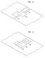
- metallic patches 50 serving as parasitic elements in that they are not driven by any feed network, are formed on opposite sides of the radiating patch 40.
- the longitudinal centerline of the parasitic patches 50 in the transverse direction of the antenna are a distance L (measured in units of wavelength ⁇ ) from the centerline of the radiating patch 40.
- L measured in units of wavelength ⁇
- the initial value of L is a matter of design choice.
- the parasitic patches 50 each have a width W related to the width of the radiating patch 40, but lengths substantially less than the length of the radiating patch 40. As a result, the parasitic patches 50 will affect the HP radiation pattern produced by the radiating patch 40, but not the VP radiation pattern.
- the radiating patch 40 is driven to by a test signal, and the beam width of the HP radiation pattern is measured. The measured beam width and associated values of the distance L and the width W are recorded.
- the structure of Fig. 2 is repeatedly formed, each structure having a different distance L. Again the set of distances L used is a matter of design choice. After each structure is formed, the beam width of the HP radiation pattern is recorded in association with the values of the distance L and the width W.
- the width W of the parasitic patches 50 is changed, and the procedure of (1) forming the structure of Fig. 2 for the set of distances L, (2) measuring the beam width of the HP radiation pattern for each structure and (3) recording the beam width values in association with the values of the distance L and width W is repeated. This procedure is repeated for a set of widths W; the set of width W being a matter of design choice.
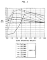
- Fig. 4 illustrates the HP radiation pattern data generated according to this procedure for an antenna portion having the structure shown in Figs. 1 and 2, wherein the radiating patch 40 had the dimensions of 0.35 ⁇ x 0.35 ⁇ . More specifically, Fig. 4 illustrates a graph of the beam width versus the distance L for parasitic patches 50 of different widths W.
- the procedure for generating the data indicating the affect parasitic elements having on the HP radiation pattern of a radiation element is then repeated for the VP radiation pattern of the radiation element.
- the parasitic patches 60 for affecting the VP radiation pattern have different dimensions than the parasitic patches 50 affecting the HP radiation pattern.
- the width of the parasitic patches 60 is substantially less than the width of the radiating patch 40 so as not to affect the HP radiation pattern. Accordingly, in repeating the data generation procedure for the VP radiation pattern, the length LG of the parasitic patches 60 is varied in the same manner that the width W of the parasitic patches 50 was varied.
- Fig. 5 illustrates the VP radiation pattern data generated for an antenna portion having the structure shown in Fig. 3, wherein the radiating patch 40 had the dimensions of 0.35 ⁇ x 0.35 ⁇ . More specifically, Fig. 5 illustrates a graph of the beam width versus the distance L for parasitic patches 60 of different lengths LG.
- this data can be generated through computer simulation.
- the antenna designer may be able to choose a single pair of parasitic elements that will produce desired beam widths in the HP and VP radiation patterns (i.e., a pair of parasitic elements having dimensions W x LG and a distance L from the radiating element to produce the desired beam widths).
- a common distance L for affecting both the HP and VP radiation pattern beam widths can not be found.
- two pairs of parasitic elements will have to be used.
- One pair of parasitic elements will be chosen from Fig. 4 to affect the HP radiation pattern beam width, and only the HP radiation pattern beam width. Accordingly, this pair of parasitic elements has a length LG substantially less than the radiating element so as not to affect the VP radiation pattern.
- Another pair of parasitic elements will be chosen from Fig. 5 to affect the VP radiation pattern beam width, and only the VP radiation pattern beam width. Accordingly, this pair of parasitic elements has a width W substantially less than the radiating element so as not to affect the HP radiation pattern.
- the pair of parasitic elements affecting the HP radiation pattern and the pair of parasitic elements affecting the VP radiation pattern will have to be offset in the longitudinal direction of the antenna from one another to prevent one set of parasitic elements from shielding, and therefore, interfering with the other set of parasitic elements. Furthermore, this offsetting of the parasitic elements may slightly change the affect on beam width and require a small change in the distance L or width W (or length LG) of the offset parasitic elements. This fine tuning of the offset parasitic elements can be performed in the same manner that the HP and VP radiation pattern data were generated.
- design methodology of the present invention was described with respect to a dual polarized antenna, the design methodology is equally applicable to a single polarization antenna.
- the radiation pattern of a radiating element can be controlled using parasitic elements.
- a desired beam width for the radiation pattern is obtained.
- the radiation patterns of different polarization are independently controlled.
Landscapes
- Variable-Direction Aerials And Aerial Arrays (AREA)
- Waveguide Aerials (AREA)
- Details Of Aerials (AREA)
Abstract
Description
Claims (15)
- A method of producing an antenna or antenna array with a desired beam width, comprising:forming a radiating element having a radiation pattern; andcontrolling the radiation pattern to have a desired beam width by forming parasitic elements in association with the radiating element.
- The method of claim 1, wherein said controlling step comprises:
forming parasitic elements of a certain size and at a certain distance from the radiating element to obtain the radiation pattern with the desired beam width. - The method of claim 1, wherein the radiating element is one of a metallic patch, printed dipole, and etched slot.
- The method of claim 1, further comprising:generating data indicative of an effect parasitic elements have on the beam width of the radiation pattern; and whereinthe controlling step controls the radiation pattern to have the desired beam width by forming parasitic elements based on the generated data.
- A method of producing a dual polarization antenna or antenna array with desired beam widths for each polarization, comprising:forming a radiating element having a first and second radiation pattern of a first and second polarization, respectively;controlling the first and second radiation patterns to have first and second desired beam widths, respectively, by forming parasitic elements in association with the radiating element.
- The method of claim 5, wherein the controlling step comprises:independently controlling the first radiation pattern to have the first desired beam width by forming first parasitic elements in association with the radiating element; andindependently controlling the second radiation pattern to have the second desired beam width by forming the second parasitic elements in association with the radiation element.
- The method of claim 6, wherein
the first controlling step includes,forming parasitic elements of a first certain size and at a first certain distance from the radiating element;the second controlling step includes,forming parasitic elements of a second certain size and a second certain distance from the radiating element. - The method of claim 6, further comprising:generating data indicative of an effect parasitic elements have on the beam width of the radiation pattern; and whereinthe independently controlling the first radiation pattern step controls the first radiation pattern to have the first desired beam width by forming parasitic elements based on the generated data; andthe independently controlling the second radiation pattern step controls the second radiation pattern to have the second desired beam width by forming parasitic elements based on the generated data.
- The method of claim 5, wherein the radiating element is one of a metallic patch, printed dipole and etched slot.
- An antenna or antenna array, comprising:a radiating element formed on a substrate; andfirst parasitic elements formed on said substrate adjacent to opposite sides of said radiating element, said first parasitic elements separated from said radiating element and dimensioned to cause said radiating element to produce a radiation pattern of a first polarization with a first desired beam width.
- The antenna of claim 10, wherein said parasitic elements are separated from said radiating element and dimensioned to cause said radiating element to produce said radiation pattern of said first polarization with said first beamwidth and to produce a radiation pattern of a second polarization with a second beam width.
- The antenna of claim 11, further comprising:
second parasitic elements formed on said substrate adjacent to opposite sides of said radiating element, said second parasitic elements separated from said radiating element and dimensioned to cause said radiating element to produce a radiation pattern of a second polarization with a second desired beam width. - The antenna of claim 12, wherein said first polarization is horizontal polarization and said second polarization is vertical polarization.
- The antenna of claim 12, wherein said second parasitic elements are separated from said first parasitic elements such that said second parasitic elements do not shield said first parasitic elements.
- The antenna of claim 12, wherein said first desired beam width equals said second desired beam width.
Applications Claiming Priority (2)
| Application Number | Priority Date | Filing Date | Title |
|---|---|---|---|
| US544117 | 2000-04-06 | ||
| US09/544,117 US6320544B1 (en) | 2000-04-06 | 2000-04-06 | Method of producing desired beam widths for antennas and antenna arrays in single or dual polarization |
Publications (2)
| Publication Number | Publication Date |
|---|---|
| EP1148582A2 true EP1148582A2 (en) | 2001-10-24 |
| EP1148582A3 EP1148582A3 (en) | 2003-12-17 |
Family
ID=24170812
Family Applications (1)
| Application Number | Title | Priority Date | Filing Date |
|---|---|---|---|
| EP01302765A Withdrawn EP1148582A3 (en) | 2000-04-06 | 2001-03-26 | Method of producing desired beam widths for antennas and antenna arrays in single or dual polarization |
Country Status (8)
| Country | Link |
|---|---|
| US (1) | US6320544B1 (en) |
| EP (1) | EP1148582A3 (en) |
| JP (1) | JP2001352215A (en) |
| KR (1) | KR20010095296A (en) |
| CN (1) | CN1320982A (en) |
| AU (1) | AU3505701A (en) |
| BR (1) | BR0101299A (en) |
| CA (1) | CA2337929A1 (en) |
Cited By (4)
| Publication number | Priority date | Publication date | Assignee | Title |
|---|---|---|---|---|
| WO2005122331A1 (en) * | 2004-06-04 | 2005-12-22 | Andrew Corporation | Directed dipole antenna |
| EP1865576A1 (en) * | 2006-06-07 | 2007-12-12 | Jaybeam Wireless SAS | A dual-polar antenna for a base station of mobile radio systems with adjustable azimuth beamwidth |
| US7358922B2 (en) | 2002-12-13 | 2008-04-15 | Commscope, Inc. Of North Carolina | Directed dipole antenna |
| WO2011073645A3 (en) * | 2009-12-14 | 2011-08-18 | Aerial Research Technology Limited | Notch antenna |
Families Citing this family (42)
| Publication number | Priority date | Publication date | Assignee | Title |
|---|---|---|---|---|
| JP2004516735A (en) * | 2000-12-21 | 2004-06-03 | アンドリュー・コーポレイション | 2-pole antenna |
| WO2003050917A1 (en) * | 2001-12-07 | 2003-06-19 | Skycross, Inc. | Multiple antenna diversity for wireless lan applications |
| US7436360B2 (en) * | 2002-04-19 | 2008-10-14 | Skycross, Inc. | Ultra-wide band monopole antenna |
| US6917334B2 (en) * | 2002-04-19 | 2005-07-12 | Skycross, Inc. | Ultra-wide band meanderline fed monopole antenna |
| WO2003103087A2 (en) * | 2002-06-04 | 2003-12-11 | Skycross, Inc. | Wideband printed monopole antenna |
| CA2489837C (en) * | 2002-06-21 | 2008-09-09 | Research In Motion Limited | Multiple-element antenna with parasitic coupler |
| US6888510B2 (en) * | 2002-08-19 | 2005-05-03 | Skycross, Inc. | Compact, low profile, circular polarization cubic antenna |
| US20040036655A1 (en) * | 2002-08-22 | 2004-02-26 | Robert Sainati | Multi-layer antenna structure |
| WO2005048398A2 (en) * | 2003-10-28 | 2005-05-26 | Dsp Group Inc. | Multi-band dipole antenna structure for wireless communications |
| JP2005210521A (en) * | 2004-01-23 | 2005-08-04 | Sony Corp | Antenna device |
| JP3903991B2 (en) * | 2004-01-23 | 2007-04-11 | ソニー株式会社 | Antenna device |
| TWI276244B (en) * | 2004-06-04 | 2007-03-11 | Wistron Neweb Corp | Wireless communication device capable of switching antennas according to data transmission information on network |
| US7113135B2 (en) * | 2004-06-08 | 2006-09-26 | Skycross, Inc. | Tri-band antenna for digital multimedia broadcast (DMB) applications |
| CN100347905C (en) * | 2004-07-22 | 2007-11-07 | 上海交通大学 | Small high directional plane double antenna |
| CN100357746C (en) * | 2004-08-17 | 2007-12-26 | 财团法人工业技术研究院 | Light Modulating Scattering Oscillator and Its Array |
| JP3800549B2 (en) * | 2004-09-14 | 2006-07-26 | 松下電器産業株式会社 | Antenna device and multi-beam antenna device |
| JP4478634B2 (en) * | 2005-08-29 | 2010-06-09 | 富士通株式会社 | Planar antenna |
| JP2008042734A (en) * | 2006-08-09 | 2008-02-21 | Nippon Electronics Service Kk | Rfid data carrier and rfid data carrier supporting member |
| US20100141532A1 (en) * | 2008-02-25 | 2010-06-10 | Jesper Uddin | Antenna feeding arrangement |
| US7864117B2 (en) * | 2008-05-07 | 2011-01-04 | Nokia Siemens Networks Oy | Wideband or multiband various polarized antenna |
| US20110063190A1 (en) * | 2009-08-26 | 2011-03-17 | Jimmy Ho | Device and method for controlling azimuth beamwidth across a wide frequency range |
| ES2591327T3 (en) * | 2010-01-08 | 2016-11-28 | Vestas Wind Systems A/S | Antenna beam control elements, systems, architectures and methods for radar, communications and other applications |
| US8854264B2 (en) * | 2011-08-22 | 2014-10-07 | Infineon Technologies Ag | Two-dimensional antenna arrays for beamforming applications |
| JP5948044B2 (en) * | 2011-11-25 | 2016-07-06 | 株式会社日立国際八木ソリューションズ | Directional antenna |
| JP5710558B2 (en) | 2012-08-24 | 2015-04-30 | 株式会社東芝 | Wireless device, information processing device and storage device including the same |
| CN103036072A (en) * | 2012-11-20 | 2013-04-10 | 江苏安特耐科技有限公司 | 2.4 gigahertz (G) double-unit vertical and horizontal dual-polarized antenna element |
| CN103036070A (en) * | 2012-11-20 | 2013-04-10 | 江苏安特耐科技有限公司 | 5.8 gigahertz (G) double-unit vertical and horizontal dual-polarized antenna element |
| US10720714B1 (en) * | 2013-03-04 | 2020-07-21 | Ethertronics, Inc. | Beam shaping techniques for wideband antenna |
| US20150029067A1 (en) * | 2013-03-13 | 2015-01-29 | Aliphcom | Rf signal pickup from an electrically conductive substrate utilizing passive slits |
| US8988298B1 (en) * | 2013-09-27 | 2015-03-24 | Qualcomm Incorporated | Collocated omnidirectional dual-polarized antenna |
| JP2015092658A (en) * | 2013-09-30 | 2015-05-14 | 京セラサーキットソリューションズ株式会社 | Antenna board |
| JP2015092653A (en) * | 2013-09-30 | 2015-05-14 | 京セラサーキットソリューションズ株式会社 | Antenna substrate |
| TWM529948U (en) * | 2016-06-01 | 2016-10-01 | 啟碁科技股份有限公司 | Communication device |
| US10320082B2 (en) | 2016-07-29 | 2019-06-11 | At&T Mobility Ii Llc | High directivity slot antenna |
| US10804592B2 (en) * | 2017-03-29 | 2020-10-13 | Central Glass Company, Limited | Antenna and window glass |
| EP3656061A1 (en) | 2017-07-17 | 2020-05-27 | Telefonaktiebolaget LM Ericsson (publ) | An antenna arrangement and method for beamforming |
| KR102511737B1 (en) * | 2018-01-24 | 2023-03-20 | 삼성전자주식회사 | Antenna structure and electronic device comprising antenna structure |
| JP7231608B2 (en) * | 2018-02-23 | 2023-03-01 | 株式会社ヨコオ | Patch antenna and vehicle antenna device |
| CN110048230B (en) * | 2019-04-22 | 2021-08-31 | 深圳市万普拉斯科技有限公司 | Compact Antenna and Mobile Terminal |
| JP6936276B2 (en) * | 2019-04-23 | 2021-09-15 | 矢崎総業株式会社 | Vehicle antenna |
| JP7418055B1 (en) | 2023-03-17 | 2024-01-19 | 株式会社九州テン | Single-sided radiating antenna and manufacturing method of single-sided radiating antenna |
| CN120127380B (en) * | 2025-05-13 | 2025-07-25 | 华为技术有限公司 | Antennas and wireless devices |
Family Cites Families (9)
| Publication number | Priority date | Publication date | Assignee | Title |
|---|---|---|---|---|
| US3183511A (en) * | 1963-03-28 | 1965-05-11 | Hughes Aircraft Co | Broadband waveguide slot radiator with mutually coupled slots of different perimeters and orientation |
| US3541559A (en) * | 1968-04-10 | 1970-11-17 | Westinghouse Electric Corp | Antenna for producing circular polarization over wide angles |
| US4370657A (en) * | 1981-03-09 | 1983-01-25 | The United States Of America As Represented By The Secretary Of The Navy | Electrically end coupled parasitic microstrip antennas |
| US4812855A (en) * | 1985-09-30 | 1989-03-14 | The Boeing Company | Dipole antenna with parasitic elements |
| US5008681A (en) * | 1989-04-03 | 1991-04-16 | Raytheon Company | Microstrip antenna with parasitic elements |
| US5061944A (en) * | 1989-09-01 | 1991-10-29 | Lockheed Sanders, Inc. | Broad-band high-directivity antenna |
| GB9002636D0 (en) * | 1990-02-06 | 1990-04-04 | British Telecomm | Antenna |
| US5220335A (en) * | 1990-03-30 | 1993-06-15 | The United States Of America As Represented By The Administrator Of The National Aeronautics And Space Administration | Planar microstrip Yagi antenna array |
| SE9700401D0 (en) * | 1997-02-05 | 1997-02-05 | Allgon Ab | Antenna operating with isolated channels |
-
2000
- 2000-04-06 US US09/544,117 patent/US6320544B1/en not_active Expired - Lifetime
-
2001
- 2001-02-23 CA CA002337929A patent/CA2337929A1/en not_active Abandoned
- 2001-03-26 EP EP01302765A patent/EP1148582A3/en not_active Withdrawn
- 2001-04-02 CN CN01112302A patent/CN1320982A/en active Pending
- 2001-04-03 BR BR0101299-1A patent/BR0101299A/en not_active Application Discontinuation
- 2001-04-04 KR KR1020010017822A patent/KR20010095296A/en not_active Withdrawn
- 2001-04-06 JP JP2001108498A patent/JP2001352215A/en active Pending
- 2001-04-06 AU AU35057/01A patent/AU3505701A/en not_active Abandoned
Cited By (5)
| Publication number | Priority date | Publication date | Assignee | Title |
|---|---|---|---|---|
| US7358922B2 (en) | 2002-12-13 | 2008-04-15 | Commscope, Inc. Of North Carolina | Directed dipole antenna |
| WO2005122331A1 (en) * | 2004-06-04 | 2005-12-22 | Andrew Corporation | Directed dipole antenna |
| EP1865576A1 (en) * | 2006-06-07 | 2007-12-12 | Jaybeam Wireless SAS | A dual-polar antenna for a base station of mobile radio systems with adjustable azimuth beamwidth |
| WO2007141281A1 (en) * | 2006-06-07 | 2007-12-13 | Jaybeam Wireless Sas | A dual-polar antenna for a base station of mobile radio systems with adjustable azimuth beamwidth |
| WO2011073645A3 (en) * | 2009-12-14 | 2011-08-18 | Aerial Research Technology Limited | Notch antenna |
Also Published As
| Publication number | Publication date |
|---|---|
| US6320544B1 (en) | 2001-11-20 |
| CN1320982A (en) | 2001-11-07 |
| EP1148582A3 (en) | 2003-12-17 |
| CA2337929A1 (en) | 2001-10-06 |
| KR20010095296A (en) | 2001-11-03 |
| BR0101299A (en) | 2001-11-06 |
| JP2001352215A (en) | 2001-12-21 |
| AU3505701A (en) | 2001-10-11 |
Similar Documents
| Publication | Publication Date | Title |
|---|---|---|
| US6320544B1 (en) | Method of producing desired beam widths for antennas and antenna arrays in single or dual polarization | |
| JP5175334B2 (en) | Polarization-dependent beam width adjuster | |
| Wang et al. | Wideband gain enhancement of high-isolation Fabry–Pérot antenna array with tandem circular parasitic patches and radial gradient PRS | |
| US9323877B2 (en) | Beam-steered wide bandwidth electromagnetic band gap antenna | |
| US6956537B2 (en) | Co-located antenna array for passive beam forming | |
| US6335703B1 (en) | Patch antenna with finite ground plane | |
| EP2917963B1 (en) | Dual polarization current loop radiator with integrated balun | |
| US6181281B1 (en) | Single- and dual-mode patch antennas | |
| AU2010322590B2 (en) | Installation method of radiating elements disposed on different planes and antenna using same | |
| Bae et al. | 5G dual (S-/Ka-) band antenna using thick patch containing slotted cavity array | |
| Zhang et al. | Scalable omnidirectional dual-polarized antenna using cavity and slot-dipole hybrid structure | |
| EP1217690B1 (en) | Dual band antenna using a single column of elliptical vivaldi notches | |
| CN104798257A (en) | Antennas for mobile communication base stations | |
| WO2006030583A1 (en) | Antenna assembly and multibeam antenna assembly | |
| CN106935982B (en) | Planar array antenna | |
| Zheng et al. | A miniaturized wideband dual-polarized antenna based on mode-control principle for base-station applications | |
| EP3642906B1 (en) | Wideband antenna array | |
| Hwang et al. | Cavity-backed stacked patch array antenna with dual polarization for mmWave 5G base stations | |
| Chen et al. | Single-layer wideband tilted beam phased array antenna for millimeter-wave vehicle communications | |
| CN111048893A (en) | Low-profile broadband dual-polarized dielectric-filled microstrip antenna | |
| US5559523A (en) | Layered antenna | |
| Zhao et al. | A beamwidth and beam direction reconfigurable antenna based on multi‐mode parasitic coupling | |
| Sohaib et al. | High gain microstrip yagi antenna for millimeter waves | |
| Rao | A single-substrate microstrip-fed slot antenna array with reduced back radiation | |
| US20260142379A1 (en) | Radiator module and antenna device for performing broadside radiation and end-fire radiation |
Legal Events
| Date | Code | Title | Description |
|---|---|---|---|
| PUAI | Public reference made under article 153(3) epc to a published international application that has entered the european phase |
Free format text: ORIGINAL CODE: 0009012 |
|
| AK | Designated contracting states |
Kind code of ref document: A2 Designated state(s): AT BE CH CY DE DK ES FI FR GB GR IE IT LI LU MC NL PT SE TR |
|
| AX | Request for extension of the european patent |
Free format text: AL;LT;LV;MK;RO;SI |
|
| PUAL | Search report despatched |
Free format text: ORIGINAL CODE: 0009013 |
|
| AK | Designated contracting states |
Kind code of ref document: A3 Designated state(s): AT BE CH CY DE DK ES FI FR GB GR IE IT LI LU MC NL PT SE TR |
|
| AX | Request for extension of the european patent |
Extension state: AL LT LV MK RO SI |
|
| 17P | Request for examination filed |
Effective date: 20040608 |
|
| AKX | Designation fees paid |
Designated state(s): DE FR GB |
|
| 17Q | First examination report despatched |
Effective date: 20040910 |
|
| STAA | Information on the status of an ep patent application or granted ep patent |
Free format text: STATUS: THE APPLICATION IS DEEMED TO BE WITHDRAWN |
|
| 18D | Application deemed to be withdrawn |
Effective date: 20050120 |