EP1148578A1 - Frequency stable resonator - Google Patents
Frequency stable resonator Download PDFInfo
- Publication number
- EP1148578A1 EP1148578A1 EP00302984A EP00302984A EP1148578A1 EP 1148578 A1 EP1148578 A1 EP 1148578A1 EP 00302984 A EP00302984 A EP 00302984A EP 00302984 A EP00302984 A EP 00302984A EP 1148578 A1 EP1148578 A1 EP 1148578A1
- Authority
- EP
- European Patent Office
- Prior art keywords
- layers
- temperature
- substrate
- dielectric
- thickness
- Prior art date
- Legal status (The legal status is an assumption and is not a legal conclusion. Google has not performed a legal analysis and makes no representation as to the accuracy of the status listed.)
- Withdrawn
Links
Images


Classifications
-
- H—ELECTRICITY
- H01—ELECTRIC ELEMENTS
- H01P—WAVEGUIDES; RESONATORS, LINES, OR OTHER DEVICES OF THE WAVEGUIDE TYPE
- H01P7/00—Resonators of the waveguide type
- H01P7/10—Dielectric resonators
-
- Y—GENERAL TAGGING OF NEW TECHNOLOGICAL DEVELOPMENTS; GENERAL TAGGING OF CROSS-SECTIONAL TECHNOLOGIES SPANNING OVER SEVERAL SECTIONS OF THE IPC; TECHNICAL SUBJECTS COVERED BY FORMER USPC CROSS-REFERENCE ART COLLECTIONS [XRACs] AND DIGESTS
- Y10—TECHNICAL SUBJECTS COVERED BY FORMER USPC
- Y10S—TECHNICAL SUBJECTS COVERED BY FORMER USPC CROSS-REFERENCE ART COLLECTIONS [XRACs] AND DIGESTS
- Y10S505/00—Superconductor technology: apparatus, material, process
- Y10S505/70—High TC, above 30 k, superconducting device, article, or structured stock
-
- Y—GENERAL TAGGING OF NEW TECHNOLOGICAL DEVELOPMENTS; GENERAL TAGGING OF CROSS-SECTIONAL TECHNOLOGIES SPANNING OVER SEVERAL SECTIONS OF THE IPC; TECHNICAL SUBJECTS COVERED BY FORMER USPC CROSS-REFERENCE ART COLLECTIONS [XRACs] AND DIGESTS
- Y10—TECHNICAL SUBJECTS COVERED BY FORMER USPC
- Y10S—TECHNICAL SUBJECTS COVERED BY FORMER USPC CROSS-REFERENCE ART COLLECTIONS [XRACs] AND DIGESTS
- Y10S505/00—Superconductor technology: apparatus, material, process
- Y10S505/825—Apparatus per se, device per se, or process of making or operating same
- Y10S505/866—Wave transmission line, network, waveguide, or microwave storage device
Definitions
- the present invention relates to a resonator for use at radio frequency (rf), especially microwave frequencies, for use in telecommunications systems.
- rf radio frequency
- Microwave resonators are commonly used at microwave frequencies in filters, etc. since circuits formed of separate inductors and capacitors cannot easily be fabricated for use at microwave frequencies.
- Microwave resonators may take a variety of forms, but a common type is a short section of transmission line, a quarter wavelength or half a wavelength long and appropriately terminated.
- the transmission line may, for example comprise coaxial cable, microstrip, in which a strip conductor is separated from a metal groundplane by a layer of dielectric, or strip line in which a central strip conductor is separated from two opposing groundplane conductors by two layers of dielectric on either side of the strip conductor.
- the invention is based on the recognition that a resonator employing superconducting films may be constructed with an extremely stable resonant frequency value for changes in temperature. Further if, as is possible with cryogenic systems, the temperature is controlled very accurately, the resonator may exhibit zero, or very close to zero change in its operating parameters over the range of the controlled temperature. In particular, it has been found for a small change in temperature, 1 mK°, that the present invention can provide a resonant frequency stable to within I part in 10 15 .
- the present invention provides an electromagnetic resonator comprising:
- the temperature dependence of the temperature compensating layers is of opposite sign to that of the substrate.
- first and second conductive layers are formed on the outer surfaces of the respective first and second temperature compensating dielectric layers.
- the conductive layers may be a normal conductor such as copper or, as preferred, HTS superconducting layers such as YBCO.
- the parameters of the temperature compensating layers such that at a selected temperature, the first derivative with respect to temperature of the phase velocity of the electromagnetic wave propagating in the resonator is zero at the operating temperature of the resonator.
- an expression for the wave velocity is provided, the first and second temperature derivatives of this wave velocity with respect to temperature are made zero or at any rate to a non-significant value by appropriate choice of materials and layer thicknesses in accordance with the wave velocity expression.
- the resonant frequency of a superconducting planar resonator is dependent on the material properties and thicknesses of the superconductors, the dielectric substrate and the temperature compensating layers.
- the first and second derivatives with respect to temperature of a wave velocity ratio (with respect to free space) are put to zero for various combinations of material properties.
- T 60°K.
- frequency standards with stabilities of parts in 10 15 are attainable.
- the present invention provides a procedure for stabilising the resonant frequency of an electromagnetic resonator with respect to temperature comprising:
- the use of superconducting films in transmission lines has many advantages for signal processing applications such as low dispersion, low loss, and wide bandwidth.
- the penetration depth and low-frequency resistance of superconducting thin films are important parameters.
- Passive microwave devices such as filters, resonators and delay lines require high-quality HTS thin films and substrate materials.
- a resonator with a temperature independent frequency is provided.
- the design depends on the material properties and thicknesses of the superconductors, the dielectric substrate, and temperature compensating dielectric layers between the substrate and the superconductors.
- the first and second derivatives of propagation phase velocity with respect to temperature are made equal to zero.
- a resonator 2 in accordance with the invention having a width Y a depth or thickness X and a predetermined length Z (for example ⁇ /2) for resonance.
- the resonator has a substrate 4 of thickness d 2 with a dielectric constant ⁇ 2 , and formed of rutile, which is a naturally occurring material consisting principally of TiO 2 .
- First and second temperature compensating dielectric layers 6 are disposed above and below substrate 4, each of thickness d 1 , having a dielectric constant ⁇ 1 , and formed of sapphire.
- superconductor layers (YBCO) 8 Disposed on the outer faces of layers 6 are superconductor layers (YBCO) 8 of thickness 1, conductivity ⁇ and penetration depth ⁇ .
- the superconductor layers 8 and layers 6 extend along the length Z of the resonator. Outside the superconductor layers 8 is disposed a dielectric 10 having a constant ⁇ 3 , which may be, for example, free space.
- the dielectric region 10 outside layers 8 is considered to be very thick so that the fields in these regions can be assumed to exponentially decay away from the interfaces. From Figure 1 , and the above assumptions, it is clear that the edge effects can be neglected, and there is no Y-dependence of the fields and currents.
- the two-fluid model is used for the superconductors, in which the total current is the sum of the supercurrent and the normal current.
- Classical skin effect and London theory are assumed for the normal current and the supercurrent, respectively.
- Equation (1) is a second-order differential equation which has two independent solutions of the form e ⁇ x and e - ⁇ x , where ⁇ is taken to be the root of ⁇ 2 with positive real part.
- the condition is a transcendental equation for which an exact solution cannot be readily obtained.
- K 1 d 1 ⁇ 1 and K 2 d 2 ⁇ 1 are employed, where K 1 and K 2 are the respective propagation constants of layers 6 and substrate 4. Physically these approximations mean that higher order modes are ignored. With small d 1 and d 2 , higher order modes will not be excited.
- the transcendental equation yields: In equation (5), the subscript 0 refers to the conductor layers 8, the subscript 1 refers to the dielectric layers 6, the subscript 2 refers to the substrate 4, and ⁇ refers to the penetration depth in superconductor layers 8.
- the wave velocity relative to that in a vacuum can be written as follows from equation (5):
- the wave is dispersionless even though there is a component of the electric field in the direction of propagation, i.e., the group velocity and phase velocity are equal and independent of frequency.
- the attenuation of the wave due to losses in each medium and the wave velocity have been obtained by replacing ⁇ 1 , ⁇ 2 and ⁇ in to their complex forms.
- the superconducting transmission resonator with temperature compensating layers shown in Figure 1 can be described by the penetration depth ⁇ of the superconductors, the dielectric constants ⁇ r of the r dielectrics, and the thicknesses d r and I of the r dielectrics and the superconductors. Where normal conductors are used the penetration depth ⁇ is replaced by the above expression.
- Figure 2 shows the first and second derivatives of propagation phase velocity as a function of temperature for a variety of temperature compensating dielectric thicknesses between 40 mm to 200 mm, where sapphire is the temperature compensating layer and rutile is the substrate dielectric material. Turning points in V r (T) can be produced close to any chosen operating temperature in this way. Temperature compensating layer thicknesses of 40, 80, 120, 160 and 200 mm are shown with the 200 mm curve being the thickest line at the top of the curve family. The lower the curve shown in Figure 2 , the smaller is the thickness of temperature compensating layer. The graphs are shown for a substrate thickness of 4.1 mm with the material rutile (rutile is a naturally occurring mineral composed principally of TiO 2 ).
- the first derivative of temperature is approximately zero. As the temperature increases, for temperature compensating layers of a very small thickness, the value of the first derivative of temperature falls to a negative value, reflecting the fact that rutile is the main influence. For a thickness of 160 mm, the first derivative of phase velocity rises slowly with increasing temperature to a maximum at around 45° K and then falls off to a negative value. For a thickness of 200 mm, the first derivative of phase velocity increases markedly to a maximum at around 60° K. It then falls off very rapidly as the temperature approaches 80° K.
- the influence of the sapphire temperature compensating layers predominates for increasing temperature to give a positive value of phase velocity, until the influence of the rutile material begins to predominate, when a maximum value of the first derivative occurs, and then for increasing temperature the first derivative goes towards a negative value.
- the second derivative of propagation phase velocity it may be seen that its value is zero or very close to zero over the range of temperatures, up to about 80° K. Thus, in this instance the second derivative will not be a significant factor in temperature variation. It is in any case a second order effect for changes in phase velocity as compared with the first derivative.
- various thicknesses of temperature compensating layers are shown, namely 200, 160, 120, 80 and 40 mm. These provide a family of curves with the thickest 200 mm layer being on top, with thinner layers producing a correspondingly lower curve. It may be seen that for both derivatives, their value remains close to zero until the thickness approaches 1 cm (values are shown in Figure 3 in meters). The curves then diverge with the thickest temperature compensating layer of 200 mm increasing greatly as the substrate thickness approaches 10 cm.
- V r (T) can be produced at desired temperatures with any chosen substrate's thickness in this way.
- the accuracy of the resonant frequency will depend on the range of temperatures to which the resonator is held. If, as with some cryogenic equipment, there is a range of operating temperatures of the order of 1°K, then the accuracy of the resonant frequency will be reduced as compared to that which is achievable when the temperature range is much more closely controlled.
- the first and second derivatives with respect to temperature of a wave velocity ratio (with respect to free space) for various combinations of material properties are put to zero.
- the dependence of resonant frequency on the dielectric constant and thicknesses of the substrate and temperature compensating layers is disclosed.
- T 60 K
- 0.1 mK frequency standards with stabilities of parts in 10 15 are attainable.
Abstract
Description
- The present invention relates to a resonator for use at radio frequency (rf), especially microwave frequencies, for use in telecommunications systems.
- Resonators are commonly used at microwave frequencies in filters, etc. since circuits formed of separate inductors and capacitors cannot easily be fabricated for use at microwave frequencies. Microwave resonators may take a variety of forms, but a common type is a short section of transmission line, a quarter wavelength or half a wavelength long and appropriately terminated. The transmission line may, for example comprise coaxial cable, microstrip, in which a strip conductor is separated from a metal groundplane by a layer of dielectric, or strip line in which a central strip conductor is separated from two opposing groundplane conductors by two layers of dielectric on either side of the strip conductor.
- The properties of transmission lines employing superconductive films as conductive plates have been studied. Superconducting films commonly employ high temperature superconductors (HTS) such as YBCO. Commonly, these have a critical temperature in a range which terminates above 100° K. In practice such films operate with cryogenic systems employing liquid nitrogen and operating at a temperature of 77° K, the boiling point of liquid nitrogen. The properties of superconducting films in transmission lines, and the temperature dependence of the constituents of such transmission lines, are discussed in the following references:
- [1] Abbas F; and Davis L E; "Propagation coefficient in a superconducting asymmetric parallelplate transmission line with buffer layer", J. Appl. Phys. 73, pp. 4494-4499, 1993.
- [2] X D Wu, A Inam, M S Hegde, B Wilkens, C C Chang, D M Hwang, L Nazar, T Venkatersan, S Miura, S Matsubara, Y Miyasaka, Appl. Phys. Lett. 54, 754 (1989).
- [3] S Y Lee and H H Park, J. Superconductivity, 9, 545 (1996).
- [4]N F Mott, Advances Phys. 39, 55 (1990).
- [5] C Gallop, C D Langham, L Hao and Farhat Abbas, IEEE Trans. Instrument. and Measurement. 46, (1997).
-
- The invention is based on the recognition that a resonator employing superconducting films may be constructed with an extremely stable resonant frequency value for changes in temperature. Further if, as is possible with cryogenic systems, the temperature is controlled very accurately, the resonator may exhibit zero, or very close to zero change in its operating parameters over the range of the controlled temperature. In particular, it has been found for a small change in temperature, 1 mK°, that the present invention can provide a resonant frequency stable to within I part in 1015.
- It has been further recognised that the present invention is applicable more generally to resonators which employ normally conductive. Further, it has been recognised that it is not necessary to employ conductive layers at all to achieve the beneficial effects of the invention.
- The present invention provides an electromagnetic resonator comprising:
- a dielectric substrate of predetermined material having a predetermined width and thickness, and having a predetermined length in the direction of propagation for achieving a desired resonance;
- first and second temperature compensating dielectric layers on two opposite faces of the substrate and extending along the length of the substrate, the dielectric layers being of a predetermined material and having a predetermined thickness; and
- the arrangement being such that the wave velocity of the resonator is dependent on the parameters of the substrate and first and second temperature compensating layers whereby the temperature dependence of the frequency of resonance of the resonator can be maintained within a predetermined range over a predetermined temperature range.
-
- As preferred, the temperature dependence of the temperature compensating layers is of opposite sign to that of the substrate.
- As preferred, first and second conductive layers are formed on the outer surfaces of the respective first and second temperature compensating dielectric layers. The conductive layers may be a normal conductor such as copper or, as preferred, HTS superconducting layers such as YBCO.
- As will be shown below, it is desirable to select the parameters of the temperature compensating layers such that at a selected temperature, the first derivative with respect to temperature of the phase velocity of the electromagnetic wave propagating in the resonator is zero at the operating temperature of the resonator.
- In accordance with a preferred form of the invention, an expression for the wave velocity is provided, the first and second temperature derivatives of this wave velocity with respect to temperature are made zero or at any rate to a non-significant value by appropriate choice of materials and layer thicknesses in accordance with the wave velocity expression. Thus, the resonant frequency of a superconducting planar resonator is dependent on the material properties and thicknesses of the superconductors, the dielectric substrate and the temperature compensating layers. As preferred, the first and second derivatives with respect to temperature of a wave velocity ratio (with respect to free space) are put to zero for various combinations of material properties. For YBCO thin films on rutile with sapphire temperature compensating layers a turning point can be realised at T = 60°K. As the temperature in cryogenic systems can be controlled to better than 0.1° mK, then frequency standards with stabilities of parts in 1015 are attainable.
- In a further aspect, the present invention provides a procedure for stabilising the resonant frequency of an electromagnetic resonator with respect to temperature comprising:
- providing a dielectric substrate of predetermined width and thickness, of predetermined length in the direction of propagation for achieving a desired resonance, and having a dielectric constant;
- providing first and second dielectric layers on two opposite faces of the substrate and
- extending along the length of the substrate, each layer having a thickness and a dielectric constant;
- providing first and second conducting layers on the outer surfaces of the first and second dielectric layers having a thickness and a penetration depth for electromagnetic fields; and
- selecting materials, thicknesses and dielectric constants of one or more of the aforesaid layers in relation to the thickness and dielectric constant of the substrate so as to achieve a desired stability in resonant frequency over a range of temperatures.
-
- A preferred embodiment of the invention will now be described with reference to the accompanying drawings wherein:
- Figure 1 is a schematic sectional view of a superconducting microwave resonator in accordance with the invention;
- Figure 2 is a graph showing first and second derivatives of propagation phase velocity as a function of temperature for a variety of temperature compensating layer thicknesses of the device of Figure 1; and
- Figure 3 is a graph of second and first derivatives of propagation phase velocity with respect to temperature as a function of the thickness of the substrate of the device of Figure 1.
-
- The use of superconducting films in transmission lines has many advantages for signal processing applications such as low dispersion, low loss, and wide bandwidth. The penetration depth and low-frequency resistance of superconducting thin films are important parameters.
- Passive microwave devices such as filters, resonators and delay lines require high-quality HTS thin films and substrate materials.
- Attempts to grow HTS films directly onto high-quality substrate materials have encountered some serious problems, due to large mismatches of both lattice constants and thermal expansion coefficients of the HTS films and some substrate materials. Also, the interdiffusion between the HTS films and substrate materials has been found to severely degrade the superconducting properties - see References [1], [2], [3].
- In this invention, a resonator with a temperature independent frequency is provided. The design depends on the material properties and thicknesses of the superconductors, the dielectric substrate, and temperature compensating dielectric layers between the substrate and the superconductors. The first and second derivatives of propagation phase velocity with respect to temperature are made equal to zero.
- Referring to Figure 1, there is shown a resonator 2 in accordance with the invention having a width Y a depth or thickness X and a predetermined length Z (for example λ/2) for resonance. The resonator has a substrate 4 of thickness d2 with a dielectric constant ε2, and formed of rutile, which is a naturally occurring material consisting principally of TiO2. First and second temperature compensating dielectric layers 6 are disposed above and below substrate 4, each of thickness d1, having a dielectric constant ε 1, and formed of sapphire. Disposed on the outer faces of layers 6 are superconductor layers (YBCO) 8 of thickness 1, conductivity σ and penetration depth λ. The superconductor layers 8 and layers 6 extend along the length Z of the resonator. Outside the superconductor layers 8 is disposed a dielectric 10 having a constant ε 3, which may be, for example, free space.
- Consider the propagation of an electromagnetic wave in the z-direction of the resonator shown in Figure 1. It is assumed that the dielectric thicknesses (d1 and d2) and the penetration depth λ of the high temperature superconductors are very small compared to the width Y of the resonator, which in turn is very small compared to the length Z of the resonator.
- The dielectric region 10 outside layers 8 is considered to be very thick so that the fields in these regions can be assumed to exponentially decay away from the interfaces. From Figure 1, and the above assumptions, it is clear that the edge effects can be neglected, and there is no Y-dependence of the fields and currents.
- The two-fluid model is used for the superconductors, in which the total current is the sum of the supercurrent and the normal current. Classical skin effect and London theory are assumed for the normal current and the supercurrent, respectively.
- Considering a TM wave:where, for the dielectrics:
 where normal conductors are employed:
- Here, α is the propagation constant along the z direction (taking), ω is the angular frequency (assuming
 ), εo and µo are the permittivity and the permeability of vacuum respectively, εr is the dielectric constant of the dielectrics, λ and σ are the penetration depth and the conductivity of the superconductors, respectively. Equation (1) is a second-order differential equation which has two independent solutions of the form eκx and e-κx, where κ is taken to be the root of κ2 with positive real part. In the positive x-direction of the dielectric, region 10, we take only the solution e-K 3 x, and in the negative x-direction we take only the solution eK 3 x, discarding eK 3 x for positive x-direction, and e-K 3 x for negative x-direction. In the superconductors, the temperature compensating dielectric layers 6, and in the substrate 4, both solutions are retained in order to satisfy the boundary conditions. In the normal or superconductors 8, and in dielectrics 4, 6, we need both solutions in order to satisfy the boundary conditions. With these solutions in the various media, we have twelve arbitrary constants for the amplitudes of the fields (one each in the dielectric region 10, two each in the superconductors 8, the temperature compensating dielectric layers 6 and the substrate 4). There are twelve boundary conditions that must be satisfied, namely the continuity of the tangential fields
Ez andHy at the six boundaries shown in Figure 1. If we ignore any nonlinearity in the system, the characteristics of the resonator are independent of the amplitude of the wave, and eleven of the constants can be determined in terms of the twelfth by using eleven of the twelve boundary conditions. The twelfth boundary condition gives an equation for the propagation constant α, which must be satisfied in order for a solution to exist. - The condition is a transcendental equation for which an exact solution cannot be readily obtained. The approximations K1d1<<1 and K2d2<<1 are employed, where K1 and K2 are the respective propagation constants of layers 6 and substrate 4. Physically these approximations mean that higher order modes are ignored. With small d1 and d2, higher order modes will not be excited. With these assumptions, the transcendental equation yields:In equation (5), the subscript 0 refers to the conductor layers 8, the subscript 1 refers to the dielectric layers 6, the subscript 2 refers to the substrate 4, and λ refers to the penetration depth in superconductor layers 8. For normal conductor layers, such as copper, the penetration depth λ should be replaced by the factor

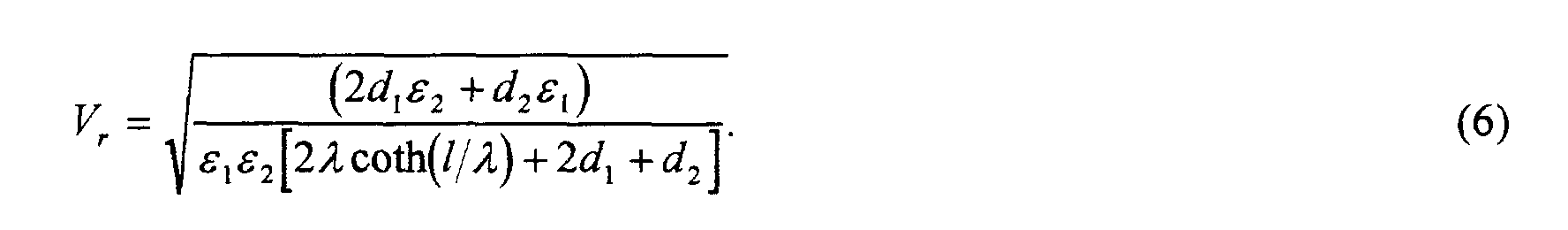
- According to equation (6), the wave is dispersionless even though there is a component of the electric field in the direction of propagation, i.e., the group velocity and phase velocity are equal and independent of frequency. The attenuation of the wave due to losses in each medium and the wave velocity have been obtained by replacing ε1, ε2 and λ in to their complex forms.
- Thus, it may be seen the superconducting transmission resonator with temperature compensating layers shown in Figure 1 can be described by the penetration depth λ of the superconductors, the dielectric constants εr of the r dielectrics, and the thicknesses dr and I of the r dielectrics and the superconductors. Where normal conductors are used the penetration depth λ is replaced by the above expression.
- The temperature dependence of the penetration depth λ of a superconductor can be described by any one of several models outlined in Reference [4] Any of those models can be used in our analysis. However, we will concentrate on the following approximate result:
- In equation (7), if the Gorter and Casimir model is assumed, then p = 4. However, recently (Ref. 4), the spin-polaron theory of high-Tc superconductivity has been explored, in which the charge carriers in a high-Tc superconductor are considered as biholes obeying the Bose-Einstein statistics and localised within a unit cell of the crystal lattice. If the charge carrier system in a high-Tc superconductor is considered as an ideal Bose-Einstein gas, then p = 1.5. Using the Gorter and Casimir model, the variations of the first and second derivatives of Vr (dVr/dT and d2Vrr/dT2) with respect to temperature for varying dielectric thicknesses of the temperature compensating layers are shown. The temperature dependence of the εr can be approximated -Reference [5] - as ε1 = 9.2+2.5x10⁻¹¹ T4 (sapphire) and ε2 = 113.446+0.043T-0.002T2+7.724x10⁻⁶T3-1.072x10⁻⁸T4 (rutile).
- It may be observed that the temperature dependence of ε 1 is of opposite sign to that of ε2.
- To provide a resonator with a temperature independent frequency, or a transmission line with temperature independent propagation constant (and therefore phase shift) along the line, it is necessary to choose a configuration of substrate and temperature compensating layers which will cause the propagation velocity (or equivalently the transmission line wavelength) to be as independent of temperature variations as possible at the selected operating temperature.
- Expanding expression (6) in a Taylor series about the operating temperature T0 leads to:
- Figure 2 shows the first and second derivatives of propagation phase velocity as a function of temperature for a variety of temperature compensating dielectric thicknesses between 40 mm to 200 mm, where sapphire is the temperature compensating layer and rutile is the substrate dielectric material. Turning points in Vr(T) can be produced close to any chosen operating temperature in this way. Temperature compensating layer thicknesses of 40, 80, 120, 160 and 200 mm are shown with the 200 mm curve being the thickest line at the top of the curve family. The lower the curve shown in Figure 2, the smaller is the thickness of temperature compensating layer. The graphs are shown for a substrate thickness of 4.1 mm with the material rutile (rutile is a naturally occurring mineral composed principally of TiO2).
- It will be seen for very low values of temperature the first derivative of temperature is approximately zero. As the temperature increases, for temperature compensating layers of a very small thickness, the value of the first derivative of temperature falls to a negative value, reflecting the fact that rutile is the main influence. For a thickness of 160 mm, the first derivative of phase velocity rises slowly with increasing temperature to a maximum at around 45° K and then falls off to a negative value. For a thickness of 200 mm, the first derivative of phase velocity increases markedly to a maximum at around 60° K. It then falls off very rapidly as the temperature approaches 80° K. Thus, it may be seen for the thicker layers the influence of the sapphire temperature compensating layers predominates for increasing temperature to give a positive value of phase velocity, until the influence of the rutile material begins to predominate, when a maximum value of the first derivative occurs, and then for increasing temperature the first derivative goes towards a negative value.
- For the second derivative of propagation phase velocity, it may be seen that its value is zero or very close to zero over the range of temperatures, up to about 80° K. Thus, in this instance the second derivative will not be a significant factor in temperature variation. It is in any case a second order effect for changes in phase velocity as compared with the first derivative.
- In Figure 3 the first and second derivatives of propagation phase velocity with respect to T, at T = 60 has been computed as a function of substrate thickness (d2) for a variety of temperature compensating layer thicknesses (d1), assuming sapphire as the temperature compensating layer and rutile as the main dielectric material. As with Figure 2, various thicknesses of temperature compensating layers are shown, namely 200, 160, 120, 80 and 40 mm. These provide a family of curves with the thickest 200 mm layer being on top, with thinner layers producing a correspondingly lower curve. It may be seen that for both derivatives, their value remains close to zero until the thickness approaches 1 cm (values are shown in Figure 3 in meters). The curves then diverge with the thickest temperature compensating layer of 200 mm increasing greatly as the substrate thickness approaches 10 cm.
- Thus, it may be seen by appropriate selection of substrate thickness and temperature compensating layer thickness, together with appropriate choice of materials, turning points in the derivatives of phase velocity with respect to temperature can be produced at any desired temperature. In the above, the influence of the conductive layer has not been discussed, but this provides a further variable for adjusting the temperature response of the resonator, for example by changing the precise constituents of YBCO, or changing the thickness of the conductive layers.
- Turning points in Vr(T) can be produced at desired temperatures with any chosen substrate's thickness in this way. Clearly, the accuracy of the resonant frequency will depend on the range of temperatures to which the resonator is held. If, as with some cryogenic equipment, there is a range of operating temperatures of the order of 1°K, then the accuracy of the resonant frequency will be reduced as compared to that which is achievable when the temperature range is much more closely controlled.
- In this invention, at least in the preferred embodiment, the first and second derivatives with respect to temperature of a wave velocity ratio (with respect to free space) for various combinations of material properties are put to zero. The dependence of resonant frequency on the dielectric constant and thicknesses of the substrate and temperature compensating layers is disclosed. An example of YBCO thin films on rutile with sapphire temperature compensating layers is provided. From this example, it may be concluded that if a turning point can be realised at T = 60 K, and the temperature controlled to better than 0.1 mK, then frequency standards with stabilities of parts in 1015 are attainable. Thus, there is disclosed a new class of planar microwave components which are ultra stable in frequency with temperature.
Claims (12)
- An electromagnetic resonator (2) comprising a dielectric substrate (4) of a predetermined material having a width (Y) and thickness (X), and having a predetermined length (Z) in the direction of propagation for achieving a desired resonance;first and second temperature compensating dielectric layers (6) on two opposite faces of the substrate and extending along the length of the substrate, the temperature compensating dielectric layers being of a predetermined material and having a predetermined thickness; andthe arrangement being such that the wave velocity of the resonator is dependent on the parameters of the substrate and first and second temperature compensating layers whereby the temperature dependence of the frequency of resonance of the resonator can be maintained within a predetermined range over a predetermined temperature range.
- A resonator according to claim 1, including first and second conductive layers (8) formed on the outer surfaces of the first and second temperature compensating dielectric layers and having a predetermined thickness.
- A resonator according to claim 2, wherein the conductive layers are superconducting layers, and wherein the wave velocity of the resonator is as follows:wherein λ is the penetration depth within the superconducting layer and ε 1 d1, ε 2 d2 are the values of dielectric constant and thickness for the substrate and temperature compensating layers.

- A resonator according to claim 2, wherein the conductive layers are of a normally conductive material, and wherein the wave velocity of the resonator is as follows:wherein ε1 d1 , ε2 d2 are the values of dielectric constant and thickness for the substrate and temperature compensating layers, and wherein β is given by the expression

- A resonator according to any preceding claim, wherein the arrangement is such that the first derivative with respect to temperature of the wave velocity is chosen to be substantially zero over a desired range of operating temperatures.
- A resonator according to any preceding claim, wherein the second derivative with respect to temperature of the wave velocity is chosen to be substantially zero over the desired operating temperature range.
- A resonator according to any preceding claim, wherein the operating temperature range is of the order of 1 mK0.
- A resonator according to any preceding claim, wherein the temperature dependence of the substrate dielectric material is of opposite sign to that of the temperature compensating layers' dielectric material at the desired operating temperature.
- A resonator according to any preceding claim, wherein the substrate is rutile, comprising principally TiO2.
- A resonator according to any preceding claim, wherein the temperature compensating layers comprise sapphire.
- An electromagnetic resonator (2) comprising a dielectric substrate (4) of predetermined width (Y) and thickness (X), and having a predetermined length (Z) in the direction of propagation for achieving a desired resonance;first and second dielectric layers (6) on two opposite faces of the substrate and extending along the length of the substrate, the dielectric layers having a predetermined thickness;first and second superconducting layers (8) formed on the outer surfaces of the first and second dielectric layers and having a predetermined thickness; andthe arrangement being such that the wave velocity Vr of electromagnetic waves propagating along the length of the substrate is given as follows:wherein λ is the penetration depth within the superconducting layer and ε 1 d1 , ε 2 d2 are the values of dielectric constant and thickness for the substrate and temperature compensating layers, whereby the resonant frequency of the resonator may be stabilised over a given temperature range by making the derivative of Vr with respect to temperature zero or close to zero within the temperature range, by appropriate choice of the parameters of Vr.

- A procedure for stabilising the resonant frequency of an electromagnetic resonator with respect to temperature comprising;providing a dielectric substrate of predetermined width and thickness, of predetermined length in the direction of propagation for achieving a desired resonance, and having a dielectric constant;providing first and second dielectric layers on two opposite faces of the substrate and extending along the length of the substrate, each layer having thickness and a dielectric constant;providing first and second conducting layers on the outer surfaces of the first and second dielectric layers having a thickness and a penetration depth for electromagnetic fields; andselecting materials, thicknesses and dielectric constants of one or more of the aforesaid layers in relation to the thickness and dielectric constant of the substrate so as to achieve a desired stability in resonant frequency over a desired range of temperature.
Priority Applications (2)
| Application Number | Priority Date | Filing Date | Title |
|---|---|---|---|
| EP00302984A EP1148578A1 (en) | 2000-04-07 | 2000-04-07 | Frequency stable resonator |
| US09/825,030 US6580933B2 (en) | 2000-04-07 | 2001-04-03 | Frequency stable resonator with temperature compensating layers |
Applications Claiming Priority (1)
| Application Number | Priority Date | Filing Date | Title |
|---|---|---|---|
| EP00302984A EP1148578A1 (en) | 2000-04-07 | 2000-04-07 | Frequency stable resonator |
Publications (1)
| Publication Number | Publication Date |
|---|---|
| EP1148578A1 true EP1148578A1 (en) | 2001-10-24 |
Family
ID=8172901
Family Applications (1)
| Application Number | Title | Priority Date | Filing Date |
|---|---|---|---|
| EP00302984A Withdrawn EP1148578A1 (en) | 2000-04-07 | 2000-04-07 | Frequency stable resonator |
Country Status (2)
| Country | Link |
|---|---|
| US (1) | US6580933B2 (en) |
| EP (1) | EP1148578A1 (en) |
Citations (3)
| Publication number | Priority date | Publication date | Assignee | Title |
|---|---|---|---|---|
| US4580116A (en) * | 1985-02-11 | 1986-04-01 | The United States Of America As Represented By The Secretary Of The Army | Dielectric resonator |
| US4661790A (en) * | 1983-12-19 | 1987-04-28 | Motorola, Inc. | Radio frequency filter having a temperature compensated ceramic resonator |
| WO1995034096A1 (en) * | 1994-06-03 | 1995-12-14 | E.I. Du Pont De Nemours And Company | Fluoropolymer protectant layer for high temperature superconductor film and photo-definition thereof |
Family Cites Families (2)
| Publication number | Priority date | Publication date | Assignee | Title |
|---|---|---|---|---|
| US5889449A (en) * | 1995-12-07 | 1999-03-30 | Space Systems/Loral, Inc. | Electromagnetic transmission line elements having a boundary between materials of high and low dielectric constants |
| JPH09246803A (en) * | 1996-03-01 | 1997-09-19 | Murata Mfg Co Ltd | Integrated dielectric line type nrd line superconducting band pass filter |
-
2000
- 2000-04-07 EP EP00302984A patent/EP1148578A1/en not_active Withdrawn
-
2001
- 2001-04-03 US US09/825,030 patent/US6580933B2/en not_active Expired - Fee Related
Patent Citations (3)
| Publication number | Priority date | Publication date | Assignee | Title |
|---|---|---|---|---|
| US4661790A (en) * | 1983-12-19 | 1987-04-28 | Motorola, Inc. | Radio frequency filter having a temperature compensated ceramic resonator |
| US4580116A (en) * | 1985-02-11 | 1986-04-01 | The United States Of America As Represented By The Secretary Of The Army | Dielectric resonator |
| WO1995034096A1 (en) * | 1994-06-03 | 1995-12-14 | E.I. Du Pont De Nemours And Company | Fluoropolymer protectant layer for high temperature superconductor film and photo-definition thereof |
Non-Patent Citations (1)
| Title |
|---|
| ABBAS F ET AL: "ULTRA-HIGH-Q RESONATORS FOR LOW-NOISE, MICROWAVE SIGNAL GENERATION USING SAPPHIRE BUFFER LAYERS AND SUPERCONDUCTING THIN FILMS", SUPERCONDUCTOR SCIENCE AND TECHNOLOGY,GB,IOP PUBLISHING, TECHNO HOUSE, BRISTOL, vol. 7, no. 7, 1 July 1994 (1994-07-01), pages 495 - 501, XP000455249, ISSN: 0953-2048 * |
Also Published As
| Publication number | Publication date |
|---|---|
| US20020014928A1 (en) | 2002-02-07 |
| US6580933B2 (en) | 2003-06-17 |
Similar Documents
| Publication | Publication Date | Title |
|---|---|---|
| EP1008234B1 (en) | High temperature superconducting structures and methods for high q, reduced intermodulation structures | |
| JP4021844B2 (en) | Tunable ferroelectric resonator device | |
| Miranda et al. | Design and development of ferroelectric tunable microwave components for Kuand K-band satellite communication systems | |
| Findikoglu et al. | Tunable and adaptive bandpass filter using a nonlinear dielectric thin film of SrTiO3 | |
| AU680866B2 (en) | Tunable microwave devices incorporating high temperature superconducting and ferroelectric films | |
| Subramanyam et al. | A K-band tunable microstrip bandpass filter using a thin-film conductor/ferroelectric/dielectric multilayer configuration | |
| EP0832507B1 (en) | Tunable microwave devices | |
| Anlage et al. | Measurements of the magnetic penetration depth in YBa2Cu3O7− δ thin films by the microstrip resonator technique | |
| Miranda et al. | Thin film multilayer conductor/ferroelectric tunable microwave components for communication applications | |
| Gough et al. | High Tc coplanar resonators for microwave applications and scientific studies | |
| Kuanr et al. | High-frequency magnetic microstrip local bandpass filters | |
| JPH08125415A (en) | Variable superconducting delay line | |
| EP1148578A1 (en) | Frequency stable resonator | |
| Romanofsky et al. | A cryogenic GaAs PHEMT/ferroelectric Ku-band tunable oscillator | |
| Basovich et al. | Parallel-plate resonator of variable spacer thickness for accurate measurements of surface impedance of high-T c superconductive films | |
| Kain et al. | Impact of kinetic inductance effect on high‐Tc | |
| US20020005766A1 (en) | RF resonator | |
| Chaloupka et al. | New experimental results for microwave conductivity of high-T/sub c/superconductors and consequences for applications to linear devices | |
| Abbas | Frequency stable superconducting resonator with buffer layers | |
| Van Keuls et al. | Influence of the biasing scheme on the performance of Au/SrTiO3/LaAlO3 thin film conductor/ferroelectric tunable ring resonators | |
| Rauch et al. | Planar transmission line resonators from YBa/sub 2/Cu/sub 3/O/sub 7-x/thin films and epitaxial SIS multilayers | |
| Abbas et al. | Ultra-high-Q resonators for low-noise, microwave signal generation using sapphire buffer layers and superconducting thin films | |
| Liu et al. | Fundamental of HTS materials and microwave filter design | |
| Withers | Passive Microwave Devices and Their Applications | |
| Abbas | Ultra Frequency Stable Electrical Components for Wireless Communications |
Legal Events
| Date | Code | Title | Description |
|---|---|---|---|
| PUAI | Public reference made under article 153(3) epc to a published international application that has entered the european phase |
Free format text: ORIGINAL CODE: 0009012 |
|
| AK | Designated contracting states |
Kind code of ref document: A1 Designated state(s): GB Kind code of ref document: A1 Designated state(s): AT BE CH CY DE DK ES FI FR GB GR IE IT LI LU MC NL PT SE |
|
| AX | Request for extension of the european patent |
Free format text: AL;LT;LV;MK;RO;SI |
|
| 17P | Request for examination filed |
Effective date: 20020412 |
|
| AKX | Designation fees paid |
Free format text: GB |
|
| REG | Reference to a national code |
Ref country code: DE Ref legal event code: 8566 |
|
| STAA | Information on the status of an ep patent application or granted ep patent |
Free format text: STATUS: THE APPLICATION HAS BEEN WITHDRAWN |
|
| 18W | Application withdrawn |
Effective date: 20040308 |