TECHNICAL FIELD
The present invention relates to a method of driving a liquid crystal
display panel which includes color filters and performs a color display,
wherein the number of display colors is reduced and limited, and further, a
driving signal is stopped to reduce the power consumption of the liquid
crystal display panel, thereby enabling low power consumption. Further, the
present invention relates to a method of controlling a display of a timepiece to
which reduction in power consumption is strongly required, wherein a liquid
crystal display panel thereof is driven by the above-described driving method.
BACKGROUND TECHNOLOGY
As a method of driving a liquid crystal display panel including: signal
electrodes provided on a first substrate; opposed electrodes provided on a
second substrate; color filters provided on the first substrate or on the second
substrate; and a liquid crystal layer sealed between the first substrate and the
second substrate, and performing a color display by electro-optical change in
the liquid crystal layer at pixel portions constituted of intersections of the
signal electrodes and the opposed electrodes, a color display pattern signal of
applying selection signals in a time sharing manner to all the signal electrodes
which constitute the pixel portions of the liquid crystal display panel and
applying data signals to the opposed electrodes in correspondence to the
selection signals of the respective signal electrodes to thereby perform a
display, is currently used in a small-sized information device.
One color display pattern signal uses a display pattern signal of
applying gradation signals at many levels, and another uses a display pattern
signal of applying gradation signals at several levels, and, further, a color
display can be performed using a binary color display pattern signal using
only ON/OFF. Even a case where gradation signals are not applied at levels
but are applied at no levels are applied can also be regarded as gradation at
many levels. That is because the no level gradation can be regarded as
smooth gradation having a large number of gradation levels.
It should be noted that a full color display generally represents a
display to which the gradation signals having no levels are applied as
described above, but a display to which the gradation signals at many levels
are applied is also called the full color display in this Description.
Further, a liquid crystal display panel of a liquid crystal display device
having no color filter disposed has been developed, which has a display
pattern signal of applying the gradation signals at many levels or the gradation
signals at several levels, or of using only ON/OFF.
By the way, it is important for the liquid crystal display panel to have
excellent display quality. In addition, as TVs shifted from a black-and-white
display to a color display, the color display can provide variety in presentation
of information.
On the other hand, as the display is shifted from a monochrome binary
display to the gradation display at many levels, and further to the full color
display, the frequency of a signal required for the display increases and an
effective voltage applied to the liquid crystal layer decreases, bringing about a
disadvantage that a voltage to be applied to each electrode needs to be
increased.
Concerning the above, there is a method of applying signals to the
signal electrodes after executing arithmetic processing to the signals for
several rows of signal electrodes in order to reduce the voltages to be applied
to the respective electrodes, but the arithmetic processing and a memory are
necessary for the display, requiring further improvement to reduce power
consumption.
Further, as a method of solving a decrease in display contrast due to a
frame response phenomenon which occurs when using a high response super
twisted nematic (STN) liquid crystal, a mode is suggested in SID92 Digest
"Active Addressing Method for High-Contrast Video-Rate STN Display." It
is necessary to simultaneously apply voltages corresponding to orthogonal
functions to row electrodes (signal electrodes) and to apply voltages
corresponding to results of product-sum operations between display
information of the respective columns and the functions provided to the
respective row electrodes, to column electrodes (data electrodes), presenting
disadvantages of occurrence of the arithmetic processing and the switching of
signals to the data electrodes corresponding to the number of the row
electrodes to which voltages are simultaneously applied, and occurrence of
consumption of electric power due to charging and discharging currents of the
liquid crystal.
Moreover, a cellular phone or the like employs a partial display of
performing a display limited to a display such as an icon or the like during a
reception stand-by state, which causes a disadvantage that the quantity of
displayable information decreases.
Therefore, an object of the present invention is to reduce electric
power consumed by a liquid crystal display device, which includes color
filters and is capable of providing much information in a color display to a
user thereof, to increase battery life with its display quality maintained as high
as possible.
In particular, another object of the present invention is to enable
realization of both the color display and low power consumption in the liquid
crystal display device to enable a color display in a timepiece which has a
strict limitation in volume and battery capacity.
DISCLOSURE OF THE INVENTION
To achieve the above-described objects, in the present invention,
when in a color liquid crystal display panel including: a transparent first
substrate formed with a plurality of signal electrodes and a transparent second
substrate formed with a plurality of data electrodes arranged so that a face
formed with the signal electrodes and a face formed with the data electrodes
are opposed to each other; a liquid crystal layer sealed in a gap therebetween;
pixel portions respectively constituted at portions where the signal electrodes
cross over and planarly overlap the data electrodes; and color filters, in which
filters of three primary colors are alternately arranged at least at positions
corresponding to the pixel portions, provided on the first substrate or on the
second substrate, a display is performed by selectively applying a voltage
between the signal electrode and the opposed electrode to thereby change
optical characteristics of the liquid crystal layer between the signal electrode
and the opposed electrode at the pixel portion, the display is performed as
follows.
A normal color display of applying selection signals to the plurality of
signal electrodes constituting all the pixel portions of the color liquid crystal
display panel in a time sharing manner, and applying data signals to the data
electrodes in correspondence to the selection signals of the signal electrodes
to allow the color filters of the pixel portions to be individually selected; and a
color reducing display of applying selection signals in such a manner to
simultaneously select a plurality of the signal electrodes to simultaneously
select the filters of a plurality of the colors arranged at positions
corresponding to the plurality of signal electrodes; are selectively performed.
Alternatively, a normal color display of applying selection signals to
the plurality of signal electrodes constituting all the pixel portions of the color
liquid crystal display panel in a time sharing manner, and applying data
signals to the data electrodes in correspondence to the selection signals of the
signal electrodes to allow the color filters of the pixel portions to be
individually selected; and a limited color display of applying selection signals
to part of the plurality of signal electrodes in a time sharing manner, and not
applying selection signals to other signal electrodes to allow only the color
filters arranged at positions corresponding to the signal electrodes to which
the selection signals are applied to be selected; are selectively performed.
In this event, it is suitable that the driven color liquid crystal display
panel is a color liquid crystal display panel including color filters, in which
filters of three primary colors in the form of stripes are alternately arranged to
be parallel to and planarly overlap the signal electrodes, provided on the first
substrate or on the second substrate, and selection signals are applied to
simultaneously select a plurality of the signal electrodes in the color reducing
display to simultaneously select the filters of a plurality of the colors in the
form of stripes arranged to planarly overlap the plurality of signal electrodes
respectively.
Alternatively, it is suitable that selection signals are applied to part of
the plurality of signal electrodes in a time sharing manner, and no selection
signal is applied to other signal electrodes in the limited color display to allow
only the filters, out of the color filters, in the form of stripes arranged to
planarly overlap the signal electrodes respectively to which the selection
signals are applied to be selected.
Further, in the present invention, when a display is performed on the
liquid crystal display panel, a full color display of applying selection signals
to the plurality of signal electrodes constituting all the pixel portions of the
liquid crystal display panel in a time sharing manner, and applying data
signals to the data electrodes in correspondence to the selection signals of the
signal electrodes, and, further, at least one of the selection signal and data
signal serving as a gradation signal for changing at many levels optical
characteristics of the liquid crystal layer to allow the filters of three primary
colors to be individually selected including gradations required for the full
color display; and a reduced color display of reducing the number of levels of
the gradation signal to be less than that of the full color display to allow the
filters of three primary colors to be individually selected with the reduced
gradation; are selectively performed.
In this event, it is suitable that a color reducing display of applying
selection signals in such a manner to simultaneously select a plurality of the
signal electrodes to simultaneously select the filters of a plurality of the colors
arranged at positions corresponding to the plurality of signal electrodes, or a
limited color display of applying selection signals to a part of the plurality of
signal electrodes in a time sharing manner, and not applying selection signals
to other signal electrodes to allow only the color filters arranged at positions
corresponding to the signal electrodes to which the selection signals are
applied to be selected, is also allowed to be selected.
Further, in the present invention, when in a color liquid crystal display
panel including: a transparent first substrate formed with a plurality of signal
electrodes and a transparent second substrate formed with a plurality of data
electrodes arranged so that a face formed with the signal electrodes and a face
formed with the data electrodes are opposed to each other; a liquid crystal
layer sealed in a gap therebetween; pixel portions respectively constituted at
portions where the signal electrodes cross over and planarly overlap the data
electrodes; and color filters, in which filters of three primary colors in the
form of stripes are alternately arranged to be parallel to and planarly overlap
the data electrodes, provided on the first substrate or on the second substrate,
a display is performed by selectively applying a voltage between the signal
electrode and the opposed electrode to thereby change optical characteristics
of the liquid crystal layer between the signal electrode and the opposed
electrode at the pixel portion, the display is performed as follows.
A normal color display of applying selection signals to the plurality of
signal electrodes constituting all the pixel portions of the color liquid crystal
display panel in a time sharing manner, and applying data signals to the data
electrodes in correspondence to the selection signals of the signal electrodes
to allow the individual color filters of the pixel portions to be selected; and a
color display of applying selection signals in such a manner to simultaneously
select a plurality of the signal electrodes, and applying data signals to the
plurality of data electrodes in a time sharing manner to allow the filters of a
plurality of the colors in the form of stripes arranged to planarly overlap the
plurality of data electrodes respectively to be individually selected and to
reduce power consumption; are selectively performed.
Alternatively, a normal color display of applying selection signals to
the plurality of the signal electrodes constituting all the pixel portions of the
color liquid crystal display panel in a time sharing manner, and applying data
signals to the data electrodes in correspondence to the selection signals of the
signal electrodes to allow the filters of three primary colors in the form of
stripes to be individually selected; and a black-and-white display of applying
selection signals in such a manner to simultaneously select a plurality of the
signal electrodes, and simultaneously applying the same data signals to three
of the data electrodes on which the filters of three primary colors in the form
of stripes are arranged to simultaneously select the filters of three primary
colors to reduce power consumption; are selectively performed.
When the drive is performed by these methods, it is suitable that the
normal color display or the full color display, and other display are switched
according to time.
Further, it is suitable that the normal color display or the full color
display, and other display are individually performed with a display region
constituted by all the pixel portions of the color liquid crystal display panel
divided into a plurality of display regions.
Furthermore, it is suitable that the normal color display or the full
color display, and other display are switched according to a remaining
capacity of a battery or a quantity of power generation by a power generator
such as a solar cell or the like so that the normal color display or the full color
display is performed when the remaining capacity of the battery or the
quantity of power generation is larger than a predetermined capacity or
quantity, and the other display is performed when the remaining capacity of
the battery or the quantity of power generation is below the predetermined
capacity or quantity.
Moreover, in the present invention, these methods are applied to a
control of a display of a timepiece including a color liquid crystal display
panel for displaying a time or information related to a time, wherein the color
liquid crystal display panel is a liquid crystal display panel including: a
transparent first substrate formed with a plurality of signal electrodes and a
transparent second substrate formed with a plurality of data electrodes
arranged so that a face formed with the signal electrodes and a face formed
with the data electrodes are opposed to each other; a liquid crystal layer
sealed in a gap therebetween; pixel portions respectively constituted at
portions where the signal electrodes cross over and planarly overlap the data
electrodes; and color filters, in which filters of three primary colors are
alternately arranged at least at positions corresponding to the pixel portions,
provided on the first substrate or on the second substrate, and displaying the
time or information related to a time by selectively applying a voltage
between the signal electrode and the opposed electrode to thereby change
optical characteristics of the liquid crystal layer between the signal electrode
and the opposed electrode at the pixel portion.
BRIEF DESCRIPTION OF DRAWINGS
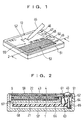
FIG. 1 is a schematic view showing a liquid crystal display device to
which a first embodiment of the present invention is applied;
FIG. 2 is a sectional view along a line 2-2 in FIG. 1;
FIG. 3 is a plan view showing a liquid crystal display panel in the
liquid crystal display device shown in FIG. 1;
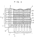
FIG. 4 is an enlarged plan view showing a part of the liquid crystal
display panel shown in FIG. 3 within a circle;
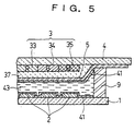
FIG. 5 is a sectional view along a line 5-5 in FIG. 4;
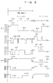
FIG. 6 is a waveform chart showing driving waveforms of the liquid
crystal display panel in the first embodiment of the present invention;
FIG. 7 is a waveform chart showing driving waveforms of the liquid
crystal display panel in a second embodiment of the present invention;
FIG. 8 is a waveform chart showing driving waveforms of the liquid
crystal display panel in a third embodiment of the present invention;
FIG. 9 is a waveform chart showing driving waveforms of the liquid
crystal display panel in a fourth embodiment of the present invention;
FIG. 10 is a waveform chart showing driving waveforms of the liquid
crystal display panel in a fifth embodiment of the present invention;
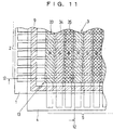
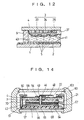
FIG. 11 is a plan view, similar to FIG. 4, of a liquid crystal display
device to which a sixth embodiment of the present invention is applied;
FIG. 12 is a sectional view along a line 12-12 in FIG. 11;
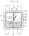
FIG. 13 is a planar schematic view of a timepiece including a liquid
crystal display panel to which a seventh embodiment of the present invention
is applied;
FIG. 14 is a sectional view along a line 14-14 in FIG. 13;
FIG. 15 is a plan view showing a liquid crystal display panel used in
the timepiece shown in FIG. 12;
FIG. 16 is a partially enlarged view of the above liquid crystal display
panel;
FIG. 17 is a planar schematic view of a timepiece including a liquid
crystal display panel to which an eighth embodiment of the present invention
is applied;
FIG. 18 is a plan view showing a liquid crystal display panel used in
the timepiece shown in FIG. 17;
FIG. 19 is a sectional view along a line 19-19 in FIG. 17;
FIG. 20 is a block diagram showing circuits for reducing the power
consumption of the timepiece shown in FIG. 17; and
FIG. 21 is a view showing an example of control of reducing power
consumption conducted with a dot matrix display portion of the timepiece
shown in FIG. 17 vertically divided.
BEST MODE FOR CARRYING OUT THE INVENTION
Hereinafter, preferred embodiments for carrying out the present
invention will be described with reference to the drawings.
First embodiment
A liquid crystal display device to which the first embodiment of the
present invention is applied will be explained first using FIG. 1 to FIG. 5.
FIG. 1 is a schematic view showing the liquid crystal display device to
which the first embodiment of the present invention is applied. FIG. 2 is a
sectional view along a line 2-2 in FIG. 1. FIG. 3 is a plan view showing a
liquid crystal display panel in the liquid crystal display device shown in FIG.
1. FIG. 4 is an enlarged plan view showing a part of the liquid crystal
display panel shown in FIG. 3 within a circle. FIG. 5 is a sectional view
along a line 5-5 in FIG. 4.
The liquid crystal display device shown in FIG. 1 is a device for
performing a display in a display region 13 with the liquid crystal display
panel, and has a scroll (+) button 46, a scroll (-) button 47, a mode switch
button 48, a power supply switch button 49 and a speaker 50 as input/output
devices or to change its display. These input/output devices are connected to
a circuit board 68 through a switch board 62 as shown in FIG. 2. A liquid
crystal display module composed of the liquid crystal display panel, a battery
64 and the input/output devices is installed within a case 51, a cover glass 58
and a case back 57, thereby constituting the liquid crystal display device.
Further, in the liquid crystal display device, a touch panel sensor, not
shown, for recognizing an input pen 45 touching the display region 13 is
provided below the cover glass 58, so that displayed information can be
selected or characters can be inputted with the input pen 45.
FIG. 1 shows a state in which a character 52 of "M" is inputted with
the input pen.
FIG. 1 also shows a state in which an upper half of the display region
13 of the liquid crystal display device is brought into a full color display
region for performing a full color display in 512 colors, while a lower half
thereof, a low power display region 53, is operated in a low power
consumption (a low power) mode to perform a monochrome display, thereby
reducing the electric power consumed by the liquid crystal display device.
Further, a low power mode display 55 for showing this state is indicated.
In the structure of the liquid crystal display panel in the liquid crystal
display device, a first substrate 1 and signal electrodes 2 are formed from the
opposite side (the back side) to the cover glass 58 as shown in FIG. 5. Red
(R) color filters 33, green (G) color filters 34 and blue (B) color filters 35 are
provided on a second substrate 4 which is opposed to the first substrate 1 with
a predetermined gap interposed therebetween. Each color filter is formed in
stripe as shown in FIG. 4. In this liquid crystal display device, the color
filters 33, 34 and 35 are in the form of stripes parallel to the signal electrodes
2. This does not cause color mixture even when the same data signals are
applied to a plurality of data electrodes as described later, thus attaining a
sharp display when using a color reducing display pattern signal, a limited
color display pattern signal, or a reduced color display pattern signal.
It should be noted that the color filters 3 may be composed of three
colors of cyan (C), magenta (M) and yellow (Y), or may be composed of
color filters in the form of dots.
An interlayer insulation film 37 made of an acrylic resin is provided
on the color filters 33, 34 and 35. Data electrodes 5 are provided on the
interlayer insulation film 37. As shown in FIG. 3, a portion where the signal
electrode 2 and the data electrode 5 overlap one another forms a pixel portion
7. A region where a plurality of the pixel portions 7 are arranged in matrix
form is the display region 13. In this liquid crystal display device, both the
signal electrodes 2 and the data electrodes 5 are in the form of stripes as
shown in FIG. 4.
A liquid crystal layer 43 is provided between the first substrate 1 and
the second substrate 4, and the liquid crystal layer 43 is sealed with a sealing
material 9 and a closing material 10. Further, alignment films 41 made of a
polyimide resin are provided on the first substrate 1 and on the second
substrate 4 respectively to align the liquid crystal layer 43 in predetermined
directions. In this embodiment, a twisted nematic liquid crystal is used as
the liquid crystal layer 43, and is aligned in a direction of 7:30 on the first
substrate 1 and in a direction of 4:30 on the second substrate 4, thereby
making a twist angle of the liquid crystal layer 43 to be 90°. However, what
is used as the liquid crystal layer 43 is not limited to the twisted nematic
liquid crystal, but another liquid crystal, for example, a guest host-type liquid
crystal, a scattering-type liquid crystal, a selective reflection-type liquid
crystal or the like may be applicable.
A first polarizing film 21 composed of RDF (trade name)
manufactured by 3M Ltd. is provided on the first substrate 1 as a reflection-type
polarizing film. A second polarizing film 22 composed of an
absorption-type polarizing film in which pigment is stretched in one direction
is provided on the second substrate 4. The first polarizing film 21 and the
second polarizing film 22 are arranged so that transmission axes thereof are
perpendicular to each other to be brought into a state of exhibiting strong
reflection characteristics when a voltage applied to the liquid crystal layer 43
is large, and exhibiting transmission characteristics when the applied voltage
is small by combination with the liquid crystal display panel. This
constitutes the liquid crystal display panel.
Further, in this liquid crystal display device, a light source 66 is
disposed on the back side of the liquid crystal display panel to allow the liquid
crystal display device to be usable in a dark environment, and the circuit
board 68 is disposed on the back side of the light source 66 as shown in FIG.
2. The liquid crystal display panel is connected to the circuit board 68 with a
zebra-rubber connector 61, and the light source 66 is connected to the circuit
board 68 through a light source terminal 67. The zebra-rubber connector is
used as the light source terminal 67, but a spring may be used.
The battery 64 is fixed to the circuit board 68 with a battery holder
spring 65, and this battery 64 is an energy source of the liquid crystal display
device. Further, the switch board 62 provided with switch buttons such as
the power supply switch button 49 or the like is connected to the circuit board
68 through a switch FPC (Flexible Print Circuit Board) 63.
The above is the structure of the liquid crystal display device to which
the first embodiment is applied, but the liquid crystal display device to which
the present invention is applied is, of course, not limited to this.
Next, a driving signal of the liquid crystal display device in this
embodiment will be explained.
A chart of driving waveforms used for the liquid crystal display
device in this embodiment is shown in FIG. 6. The horizontal axis on a
paper surface is a time axis 71, and alternating current waveforms having
positive polarity and negative polarity are applied to each screen (field) to
prevent a direct current component from being applied to the liquid crystal
layer 43. Time in a positive field is represented by Tf1(+), and time in a
negative field is represented by Tf1(-). In order to prevent flicker, Tf1
ranges from 16 milliseconds (msec.) to several milliseconds (msec.). When
Tf1 is short, the electric current consumed by the liquid crystal display device
increases due to an increase in the frequency at which the liquid crystal is
driven and an increase in the voltage applied to the liquid crystal.
The liquid crystal layer 43 composed of the twisted nematic (TN)
liquid crystal optically changes by an effective value of voltage applied
thereto per unit time. Further, since the liquid crystal layer 43 can be
described as a parallel circuit composed of a resistive component and a
capacitive component in an electric equivalent circuit, consumption by the
capacitive component occurs when the driving voltage is switched, and
consumption by the resistive component occurs while the driving voltage is
constant. An increase in the driving frequency and an increase in the driving
voltage increase power consumption also in a circuit for forming driving
waveforms.
First, a color display signal for performing a 512-color display will be
explained. This color display signal is a full color display signal capable of
performing a display at eight gradations for each color of R, G, B, and this
color display signal is also a normal color display signal because a signal
capable of individually selecting a color filter is a normal color display signal.
The normal color display signal may naturally be one having a number of
gradations fewer than that of the example shown here.
A driving voltage 81 applied to the liquid crystal layer 43 is composed
of signals at six levels of V1, V2, V3, V4, V5 and V6. In Tf1(+), a selection
signal is applied to a first signal electrode during a first selection period 74, a
selection signal is applied to a second signal electrode during a second
selection period 75, and a selection signal is applied to a third signal electrode
during a third selection period 76. The other periods in Tf1(+) are periods
during which selection signals are applied to the other signal electrodes.
For example, to the first signal electrode, a first selection signal 82 at
V6 voltage level is applied to select this electrode during the first selection
period 74, and a first non-selection signal 83 at V2 voltage level is applied
during the other periods in Tf1(+). During the periods in Tf1(-), a second
selection signal 84 at V1 voltage level is applied to the first signal electrode to
select this electrode during a first selection period, and a second non-selection
signal 85 at V5 voltage level is applied to the electrode during the other
periods in Tf1(-).
To the second signal electrode, selection periods are shifted, a
selection signal at V6 voltage level is applied during the second selection
period 75 in Tf1(+), and a non-selection signal at V2 voltage level is applied
during the other periods in Tf1(+). During the periods in Tf1(-), a second
selection signal at V1 voltage level is applied during a second selection period,
and a second non-selection signal at V5 voltage level is applied during the
other periods in Tf1(-).
Similarly, a selection signal is applied to the third signal electrode
during the third selection period 76, and a non-selection signal is applied
during the other periods, in each of Tf1(+) and Tf1(-).
Selection signals and non-selection signals are also applied to the
other signal electrodes in a similar time sharing manner, in which the
selection signals are successively applied to the signal electrodes.
A gradation signal is applied to the data electrode as the data signal to
perform the 512-color display. The driving voltage 81 is composed of six
levels of V1, V2, V3, V4, V5 and V6 as in the case of the selection signal.
The first embodiment employs pulse width modulation, in which a gradation
display is performed by changing the width ratio between a 1st-part gradation
signal and a 2nd-part gradation signal which are applied in each selection
period.
For example, in each selection period in Tf1(+), a voltage at V1 as the
1st-part gradation signal and a voltage at V4 as the 2nd-part gradation signal
are applied to the data electrode as gradation signal. In this event, a potential
difference with respect to V6, which is the voltage level of the selection signal
applied to the signal electrode, can be applied to the liquid crystal layer,
causing a large potential difference V6 - V1 during the 1st-part and a small
potential difference V6 - V4 during the 2nd-part. Therefore, by changing the
ratio between the 1st-part with the large potential difference and the 2nd-part
with the small potential difference, the quantity of charge applied to the liquid
crystal layer is changed to perform the gradation display. In other words, the
greater the width (the longer the period) of the 1st-part gradation signal is, the
brighter the display of the selected pixel becomes.
In the first example shown, a first 1st-part gradation signal 87 at V1
voltage level and a first 2nd-part gradation signal 88 at V4 voltage level are
first applied to a first data electrode during the first selection period 74. The
period of the first 1st-part gradation signal 87 is short compared to that of the
first 2nd-part gradation signal 88. Further, a second 1st-part gradation signal
89 is applied during the second selection period 75. The period of the
second 1st-part gradation signal 89 is short compared to that of the first 1st-part
gradation signal 87. Furthermore, the period of a 1st-part gradation
signal during the third selection period 76 is shorter than that of the first 1st-part
gradation signal 87 and longer than that of the second 1st-part gradation
signal 79. Therefore, the arrangement of an R filter at the first signal
electrode, a G filter at the second signal electrode, and a B filter at the third
signal electrode produces a display in red-purple. In Tf1(-), a third 1st-part
gradation signal 90 at V6 voltage level is applied during the first selection
period. The voltage level of the 2nd-part gradation signal is at V3.
In the next example shown at a different point of time, a fourth 1st-part
gradation signal 95 at V1 voltage level and a fourth 2nd-part gradation
signal 96 at V4 voltage level are applied to the first data signal during the first
selection period 74. The period of the fourth 1st-part gradation signal 95 is
long compared to that of the fourth 2nd-part gradation signal 96. Further, a
1st-part gradation signal which is short compared to the fourth 1st-part
gradation signal 95 is applied during the second selection period 75, and a 1st-part
gradation signal which is longer than the fourth 1st-part gradation signal
95 is applied during the third selection period 76. Therefore, a display in
bluish blue-purple is produced by combination with the color filters of R, G,
B. In Tf1(-), a fifth 1st-part gradation signal 97 at V6 voltage level and a
fifth 2nd-part gradation signal 98 at V1 voltage level are applied during the
first selection period.
The driving waveforms shown in the above are signal waveforms
normally used in the pulse width modulation of the liquid crystal display
device which performs the 512-color display. The example in which the
data signal is a gradation signal is described here, but it is also suitable that
gradation information is added to the selection signal to make it a gradation
signal.
Next, driving waveforms for reducing the power consumption, which
are characteristics of the present invention will be explained. The
characteristics are that selection signals are integrally and simultaneously
applied to three signal electrodes for the R, G, B color filters to select them,
and that the driving voltage is decreased. Since the R, G, B color filters are
arranged to be in the form of stripes parallel to the signal electrodes, it is
extremely easy to integrate the signal electrodes corresponding to the three
color filters. The driving waveforms explained here are a color reducing
display pattern signal for performing a color reducing display, which
simultaneously selects a plurality of the signal electrodes.
The driving voltage of a low power display is a low power driving
voltage 99 composed of six levels of Va, Vb, Vc, Vd, Ve and Vf. Even a
weak voltage can sufficiently cause an electro-optical change in the liquid
crystal layer as the selection period of the signal electrode is increased as
described later, and thus the low power driving voltage 99 is a voltage smaller
than the driving voltage 81 for the color display.
First, to the first signal electrode, a low power first selection signal
100 at Va voltage level is applied during a period corresponding to the first
selection period 74, the second selection period 75 and the third selection
period 76 in Tf1(+), and a low power first non-selection signal 101 at Ve
voltage level is applied during the other periods in Tf1(+). The same signals
as those applied to the first signal electrode are also applied to the second
signal electrode and the third signal electrode. Similarly to these three
electrodes, low power selection signals at Va voltage level are integrally
applied to every group of three out of the other signal electrodes in a time
sharing manner during the selection periods. Since the signal electrodes are
integrated in threes, the respective selection periods are three times those of
the color display and the driving frequency of the selection signal is 1/3 that
of the color display.
Also in Tf1 (-), low power second selection signals 102 at Vf voltage
level are applied during the periods of the three electrodes, and low power
second non-selection signals 103 at Vb voltage level are applied during the
other periods. Similarly to these three electrodes, low power selection
signals at Vf voltage level are integrally applied to every group of three out of
the other signal electrodes in a time sharing manner during a period three
times that of the conventional case.
The color filters R, G, B are formed on three adjacent signal
electrodes 2 as shown in FIG. 4, so that the integral selection of the three
adjacent signal electrodes results in the integral selection of the color filters R,
G, B.
The driving voltage of the data signal which is applied to the data
electrode is also at the low power driving voltage 99 composed of six levels
of Va, Vb, Vc, Vd, Ve and Vf as in the case of the selection signal.
In the first example shown, the same low power first data signal 106 at
Vf voltage level is applied to the first data electrode during the first selection
period 74, the second selection period 75 and the third selection period 76 in
Tf1(+). A low power data signal at Vf (bright) or Vc (dark) voltage level is
applied during the other periods in accordance with the display contents of
other groups of three signal electrodes.
During the periods in Tf1(-), a low power second data signal 107 at
Va voltage level or a low power data signal at Vd voltage level is applied. A
low power data signal at Va (bright) or Vd (dark) voltage level is applied
during the other periods in accordance with the display contents of other
groups of three signal electrodes.
Therefore, this case provides a monochrome black-and-white binary
display in which a group of three pixels of R, G, B simultaneously turn
ON/OFF.
In the next example shown, a low power first 1st-part gradation signal
108 at Vf voltage level and a low power first 2nd-part gradation signal 109 at
Vc voltage level are applied to the first data electrode during the first, second
and third selection periods 74, 75 and 76 in Tf1(+). A low power 1st-part
gradation signal at Vf voltage level and a low power 2nd-part gradation signal
at Vc voltage level are also applied during the other periods in accordance
with the display contents of other groups of three signal electrodes. During
the periods in Tf1(-), a low power 1st-part gradation signal at Va voltage level
and a low power 2nd-part gradation signal at Vd voltage level are applied.
For example, during the periods in Tf1(+), a potential difference with
respect to Va which is applied during the selection periods of the low power
first selection signal can be applied to the liquid crystal layer, causing a large
potential difference Va - Vf during the 1st-part period and a small potential
difference Va - Vc during the 2nd-part period. Therefore, by changing the
ratio between the 1st-part period with the large potential difference and the
2nd-part period with the small potential difference, the quantity of charge
applied to the liquid crystal layer is changed, thereby performing the
gradation display. In other words, the longer the period in which the 1st
gradation signal is applied is, the brighter display the pixel provides.
That the color filters R, G, B are integrally selected is the same as in
the example which is first shown, and thus this case provides a black-and-white
gradation display.
As is clear from the above explanation, the selection period of the
selection signal in the low power display is three times as long as that in the
state in which the 512-color display is performed. Further, since three signal
electrodes in every group are integrally selected, the voltage application
period of the data signal is also three times as long. Therefore, the driving
voltage can be reduced. Furthermore, in the first example shown, the
division of the data signal applied during each period to the 1st-part gradation
signal and 2nd-part gradation signal is stopped, and the binary display is
provided using all the periods. The switching frequency of the voltage of the
signal electrode is reduced to 1/3 as described above. Similarly, the
switching frequency of the voltage of the data signal is also reduced to 1/3.
Consequently, the power consumption can be reduced to 1/3 or less.
Further, the driving voltage can also be reduced. In the experiment,
the driving voltage could be reduced from 5.4 V to 4.25 V, and its ratio of
ON/OFF applied to the liquid crystal layer 43 could also be increased from
1.2 to 1.3.
As the results of the above, it is possible to attain the power
consumption of the liquid crystal display device being 1/4 or less that of the
conventional one. The driving voltage can be reduced to 3.85 V by
optimizing the bias ratio which is a width of a pitch of the driving voltage, so
that the power consumption becomes 1/4.2 or less. Further, as for the power
consumption of an LCD controller and driver IC for generating each signal
waveform, the frequency can be reduced to 1/3 to thereby reduce voltage,
making it possible to reduce the power consumption of a combination of the
liquid crystal and the LCD controller and driver IC to 1/10 or less. This
suppresses the consumption of the battery, providing a liquid crystal display
device friendly to the earth environment. Further, the entire display region
can be displayed, each block of the signal electrodes can be driven by low
power, and the color filters in the form of stripes corresponding to the signal
electrodes are employed, thereby attaining excellent display quality without
unevenness in display.
The gradation display is performed in the example secondly shown, in
which since the selection period of the low power selection signal is three
times as long as that of the color display pattern signal, the period of the low
power selection signal usable for the gradation of the data signal becomes
three times as long. Consequently, the applied voltage can be decreased,
resulting in reduced power consumption.
The same low power selection signals are applied to every group of
three signal electrodes in the first embodiment, but the same low power
signals may be applied to every multiple of three, for example, six or nine,
signal electrodes. The driving voltage and the power consumption can be
further reduced in this case. The ratio in number between the signal
electrodes and the data electrodes to which the same signals are applied
respectively is made 3:1, thereby realizing a display having the same aspect
ratio as that of the display using the color display pattern signal.
Second embodiment
Next, the second embodiment of the present invention will be
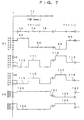
explained using FIG. 7. FIG. 7 is a chart of driving waveforms used in a
liquid crystal display device in this embodiment.
It should be noted that the liquid crystal display device used in the
second embodiment is the same as that explained in the first embodiment
except that alignment directions of a first polarizing film 21 and a second
polarizing film 22 are different from those in the first embodiment, and thus
the description except that is omitted.
In the liquid crystal display device used in this embodiment, the first
polarizing film 21 and the second polarizing film 22 are arranged so that their
transmission axes are parallel to each other, thereby providing a state of
exhibiting strong reflection characteristics when a voltage applied to a liquid
crystal layer 43 is small, and exhibiting transmission characteristics when the
applied voltage is large by combination with a liquid crystal display panel.
Also in the waveform chart in FIG. 7, the horizontal axis on a paper
surface is a time axis 71 as in FIG. 6 which is used in the description of the
first embodiment, and alternating current waveforms having positive polarity
and negative polarity are applied to each field to prevent a direct current
component from being applied to the liquid crystal layer 43. Time in a
positive field is represented by Tf1(+), and time in a negative field is
represented by Tf1(-). In order to prevent flicker, Tf1 ranges from 16
milliseconds (msec.) to several milliseconds (msec.). When Tf1 is short, the
electric current consumed by the liquid crystal display device increases due to
an increase in the frequency at which the liquid crystal is driven and an
increase in the voltage applied to the liquid crystal.
First, a color display signal for performing a 512-color display will be
explained. This color display signal, similar to that described in the first
embodiment, is a full color display pattern signal and also a normal color
display pattern signal.
A driving voltage 81 applied to the liquid crystal layer 43 is composed
of signals at six levels of V1, V2, V3, V4, V5 and V6. In Tf1(+), a selection
signal is applied to a first signal electrode during a first selection period 74, a
selection signal is applied to a second signal electrode during a second
selection period 75, and a selection signal is applied to a third signal electrode
during a third selection period 76. The other periods in Tf1(+) are periods
during which selection signals are applied to the other signal electrodes.
For example, to the first signal electrode, a first selection signal 82 at
V6 voltage level is applied to select this electrode during the first selection
period 74, and a first non-selection signal 83 at V2 voltage level is applied
during the other periods in Tf1(+). During the periods in Tf1(-), to the first
signal electrode, a second selection signal 84 at V1 voltage level is applied to
select this electrode during a first selection period, and a second non-selection
signal 85 at V5 voltage level is applied during the other periods in Tf1(-).
To the second signal electrode, selection periods are shifted, a
selection signal at V6 voltage level is applied during the second selection
period 75 in Tf1(+), and a non-selection signal at V2 voltage level is applied
during the other periods in Tf1(+). During the periods in Tf1(-), a selection
signal at V1 voltage level is applied during a second selection period, and a
non-selection signal at V5 voltage level is applied during the other periods in
Tf1(-).
Similarly, a selection signal is applied to the third signal electrode
during the third selection period, and a non-selection signal is applied during
the other periods, in each of Tf1(+) and Tf1.
Selection signals and non-selection signals are also applied to the
other signal electrodes in a similar time sharing manner, in which the
selection signals are successively applied to the signal electrodes.
A gradation signal is applied to the data electrode as the data signal
for performing a color display. The driving voltage of the data electrode is
composed of eight levels including V1 to V6 and additionally Vx1 and Vx2
as intermediate voltages. The second embodiment employs pulse height
modulation, in which a gradation display is performed by changing the
magnitude of the voltage of the gradation signal which is applied during the
selection period. In this embodiment, the greater the magnitude of the
voltage of the gradation signal, the smaller the voltage difference between the
gradation signal and the selection signal becomes during the periods in Tf1(+),
resulting in a brighter display.
In the first example shown, during the periods in Tf1(+), a sixth
gradation signal 110 at V1 voltage level is first applied to a first data electrode
during the first selection period 74. A seventh gradation signal 111 at V4
voltage level is applied during the second selection period 75, a gradation
signal at V1 voltage level is applied during the third selection period 76 as
during the first selection period 74, and individual gradation signals are
applied during the other selection periods in accordance with the respective
display contents.
Therefore, the arrangement of an R filter at the first signal electrode, a
G filter at the second signal electrode, and a B filter at the third signal
electrode produces a green display. During the periods in Tf1(-), an eighth
gradation signal 112 at V6 voltage level is applied during the first selection
period, and a ninth gradation signal 113 at V3 voltage level is applied during
the second selection period.
In the next example shown at a different point of time, during the
periods in Tf1(+), a tenth gradation signal 115 at Vx1 voltage level which is
an intermediate level between V1 and V2 is applied to the first data electrode
during the first selection period 74. Further, an eleventh gradation signal
116 at V4 voltage level is applied during the second selection period 75. A
gradation signal at Vx1 voltage level is applied during the third selection
period 76 as during the first selection period 74, and individual gradation
signals are applied during the other selection periods in accordance with the
respective display contents.
Therefore, the arrangement of an R filter at the first signal electrode, a
G filter at the second signal electrode, and a B filter at the third signal
electrode produces a display in a color of green mixed with pale red and blue.
During a period 73 in Tf1(-), a twelfth gradation signal 117 at Vx2 voltage
level is applied during the first selection period, and a thirteenth gradation
signal 118 at V3 voltage level is applied during the second selection period.
The waveforms shown in the above are waveforms normally used in
the pulse height modulation of the liquid crystal display device for performing
the 512-color display.
Next, driving waveforms for reducing the power consumption which
are characteristics of the present invention will be explained. The
characteristics are that the selection period of the signal electrode is increased,
that the driving voltage is reduced, and that the data signal is binarized. The
waveforms which are explained here are a color reducing display pattern
signal which simultaneously selects a plurality of the signal electrodes.
The driving voltage of a low power display is a low power driving
voltage 99 composed of six levels of Va, Vb, Vc, Vd, Ve and Vf. Even a
weak voltage can sufficiently cause an electro-optical change in the liquid
crystal layer as the selection period of the signal electrode is increased as
described later, and thus the low power driving voltage 99 is a voltage smaller
than the driving voltage 81 for the color display.
First, to the first signal electrode, a low power third selection signal
120 at Va voltage level is applied during a period corresponding to the first
selection period 74, the second selection period 75 and the third selection
period 76 in Tf1(+), and during the other periods in Tf1(+), a low power third
non-selection signal 121 at Ve voltage level is applied. The same signals as
those applied to the first signal electrode are also applied to the second signal
electrode and the third signal electrode. Similarly to these three electrodes,
low power selection signals at Va voltage level are integrally applied to every
group of three out of the other signal electrodes in a time sharing manner
during the selection periods. Since the signal electrodes are integrated in
threes, the respective selection periods are three times those of the full color
display and the driving frequency of the selection signal is 1/3 thereof.
Also in Tf1 (-), low power fourth selection signals 122 at Vf voltage
level are applied during the periods of the three electrodes, and low power
fourth non-selection signals 123 at Vb voltage level are applied during the
other periods. Similarly to these three electrodes, low power selection
signals at Vf voltage level are integrally applied to every group of three out of
the other signal electrodes in a time sharing manner during a period three
times that of the conventional case.
The R, G, B color filters 3 are formed on three adjacent signal
electrodes 2 as shown in FIG. 4, so that the integral selection of the three
adjacent electrodes results in the integral selection of the color filters R, G, B.
The driving voltage of the data signal which is applied to the data
electrode is also at the low power driving voltage 99 composed of six levels
of Va, Vb, Vc, Vd, Ve and Vf as in the case of the selection signal.
The same low power third data signal 124 at Vf voltage level is
applied to the first data electrode during the first selection period 74, the
second selection period 75 and the third selection period 76. A low power
data signal at Vf (dark) or Vc (bright) voltage level is applied during the other
periods in accordance with the display contents of other groups of three signal
electrodes.
Therefore, this embodiment provides a black-and-white binary display
in which a group of three pixels of R, G, B simultaneously turn ON/OFF.
During the periods in Tf1(-), a low power fourth data signal 125 at Va
voltage level or a low power data signal at Vd voltage level is applied. A
low power data signal at Va (dark) or Vd (bright) voltage level is applied
during the other periods in accordance with the display contents of other
groups of three signal electrodes.
As is clear from the above explanation, the selection period of the
signal electrode in the low power display is three times as long as that in the
state in which the 512-color display is performed. Further, since three signal
electrodes in every group are integrally selected, the voltage application
period of the data signal is also three times as long. Therefore, the driving
voltage can be reduced. Further, the switching frequency of the voltage of
the signal electrode is reduced to 1/3. Similarly, the switching frequency of
the voltage of the data signal is also reduced to 1/3. Consequently, the
power consumption can be reduced to 1/3 or less.
Further, the driving voltage can also be reduced. In the experiment,
the driving voltage could be reduced from 5.4 V to 4.25 V, and its ratio of
ON/OFF applied to the liquid crystal layer 43 could also be increased from
1.2 to 1.3.
As the results of the above, it is possible to attain the power
consumption of the liquid crystal display device being 1/4 or less that of the
conventional one. The driving voltage can be reduced to 3.85 V by
optimizing the bias ratio which is a width of a step of the driving voltage, so
that the power consumption becomes 1/4.2 or less. Further, as for the power
consumption of an LCD controller and driver IC for generating each signal
waveform, the frequency can be reduced to 1/3 to thereby reduce voltage,
making it possible to reduce the power consumption of a combination of the
liquid crystal and the LCD controller and driver IC to 1/10 or less. This
suppresses the consumption of the battery, providing a liquid crystal display
device friendly to the earth environment. Further, the entire display region
can be displayed, each block of the signal electrodes can be driven by low
power, and the color filters in the form of stripes corresponding to the signal
electrodes are employed, thereby attaining excellent display quality without
unevenness in display.
Furthermore, the use of a white display and a black display using three
colors provides a bright display and an excellent contrast ratio, thereby
making it possible to recognize the display sufficiently even in a somewhat
dark environment of the liquid crystal display device in use. Consequently,
it is possible to suppress lighting of a light source and to reduce the
illuminance of the light source. It is suitable to use means for reducing the
illuminance of the light source in combination in the case of the low power
mode.
It should be noted that the example in which the low power data signal
is binary, ON/OFF, is shown here, but it is suitable to allow the low power
data signal to take a voltage at an intermediate level between ON and OFF,
for example, Vd or Ve during the periods in Tf1(+) to perform the gradation
display.
Third embodiment
Next, the third embodiment of the present invention will be explained
using FIG. 8. FIG. 8 is a chart of driving waveforms used in a liquid crystal
display device in this embodiment.
It should be noted that the liquid crystal display device used in the
third embodiment is the same as that explained in the first embodiment, and
thus the description thereof is omitted.
Also in the waveform chart in FIG. 8, the horizontal axis on a paper
surface is a time axis 71 as in FIG. 6 which is used in the description of the
first embodiment, and alternating current waveforms having positive polarity
and negative polarity are applied to each field to prevent a direct current
component from being applied to the liquid crystal layer 43. Time in a
positive field is represented by Tf1(+), and time in a negative field is
represented by Tf1(-). In order to prevent flicker, Tf1 ranges from 16
milliseconds (msec.) to several milliseconds (msec.). When Tf1 is short, the
electric current consumed by the liquid crystal display device increases due to
an increase in the frequency at which the liquid crystal is driven and an
increase in the voltage applied to the liquid crystal.
First, a color display signal for performing a 512-color display will be
explained. This color display signal, simialr to that described in the first
embodiment, is a full color display pattern signal and also a normal color
display pattern signal.
A driving voltage 81 applied to the liquid crystal layer 43 is composed
of signals at six levels of V1, V2, V3, V4, V5 and V6. In Tf1(+), a selection
signal is applied to a first signal electrode during a first selection period 74, a
selection signal is applied to a second signal electrode during a second
selection period 75, and a selection signal is applied to a third signal electrode
during a third selection period 76. The other periods in Tf1(+) are periods
during which selection signals are applied to the other signal electrodes.
To the first signal electrode, a first selection signal 82 at V6 voltage
level is applied to select this electrode during the first selection period 74, and
a first non-selection signal 83 at V2 voltage level is applied during the other
periods in Tf1(+). During the periods in Tf1(-), a second selection signal 84
at V1 voltage level is applied to select this electrode during a first selection
period, and a second non-selection signal 85 at V5 voltage level is applied
during the other periods in Tf1(-).
To the second signal electrode, a third selection signal 131 at V6
voltage level is applied to select this electrode during the second selection
period 75, and a third non-selection signal 130 at V2 voltage level is applied
during the other periods in Tf1(+). During the periods in Tf1(-), a fourth
selection signal 133 at V1 voltage level for selecting this electrode and a
fourth non-selection signal 132 at V5 voltage level are applied.
To the third signal electrode, a fifth selection signal 136 at V6 voltage
level is applied to select this electrode during the third selection period 76 in
Tf1(+), and a fifth non-selection signal 135 at V2 voltage level is applied
during the other periods in Tf1(+). During the periods in Tf1(-), a selection
signal at V1 voltage level for selecting this electrode and a sixth non-selection
signal 137 at V5 voltage level are applied.
Selection signals and non-selection signals which are time-divided are
also applied to the other signal electrodes, in which the selection signals for
the signal electrodes are successively applied.
As described above, the selection periods of the signal electrodes are
successively delayed in a time sharing manner, and the periods other than the
selection periods are non-selection periods.
A gradation signal is applied to the data electrode as the data signal to
perform the 512-color display. The driving voltage 81 is composed of six
levels of V1, V2, V3, V4, V5 and V6 as in the case of the selection signal.
The fourth embodiment employs, as in the first embodiment, pulse width
modulation, in which a gradation display is performed by changing the width
ratio between a 1st-part gradation signal and a 2nd-part gradation signal
which are applied during the first selection period 74.
A fourteenth 1st-part gradation signal 140 at V1 voltage level and a
fourteenth 2nd-part gradation signal 141 at V4 voltage level are first applied
to the first data electrode during the first selection period 74. The period of
the fourteenth 1st-part gradation signal 140 is short compared to the period of
the fourteenth 2nd-part gradation signal 141. Further, a fifteenth 1st-part
gradation signal 142 at V1 voltage level and a 2nd-part gradation signal at V4
voltage level are applied during the second selection period 75, and a pair of
1st-part gradation signal and 2nd-part gradation signal are similarly applied
during the other selection periods. In Tf1(-), a sixteenth 1st-part gradation
signal 143 at V6 voltage level and a sixteenth 2nd-part gradation signal 144 at
V3 voltage level are applied during the first selection period. In the example
shown here, the color filters of R, G, B are arranged at the first, second and
third signal electrodes respectively, producing a dark gray display in which all
the pixels are dark.
The driving waveforms shown in the above are signal waveforms
normally used in the pulse width modulation of the liquid crystal display
device for performing the 512-color display.
Next, driving waveforms for reducing the power consumption which
are characteristics of the present invention will be explained. The
characteristics are that the data signal performs a display at only two
gradations of ON and OFF, and the selection signal performs a display with
two selected electrodes and the other non-selected one in every group of three
electrodes. It is preferable to use color filters in the form of stripes which
are arranged parallel to the signal electrodes when a character is displayed.
What is explained here is a limited color display pattern signal for performing
a limited color display in which part of the signal electrodes in a group is non-selected
or stopped.
In this embodiment, the driving voltage of a low power display is
composed of six levels of Va, Vb, Vc, Vd and Vf. Even a weak voltage can
sufficiently cause an electro-optical change in the liquid crystal layer as the
selection period of the signal electrode is increased as described later, and
thus a low power driving voltage 99 is a voltage smaller than the driving
voltage 81 for the color display.
In this embodiment, since no selection signal is applied to the third
signal electrode, selection signals may be applied to two signal electrodes of
the first signal electrode and the second signal electrode in three selection
periods of the first, second and third selection periods 74, 75 and 76.
Therefore, a low power seventh selection signal 251 at Va voltage
level is applied first to the first signal electrode during the first selection
period 74 and the first half of the second selection period 75 in Tf1(+), and a
low power seventh non-selection signal 252 at Ve voltage level is applied
during the other periods in Tf1(+). A low power ninth selection signal 256
at Va voltage level is applied to the second signal electrode during the second
half of the second selection period 75 and the third selection period in Tf1(+),
and a low power ninth non-selection signal 255 at Ve voltage level is applied
during the other periods in Tf1(+). No selection signal is applied to the third
signal electrode, but a low power non-selection signal at Ve voltage level is
applied.
As for the other signal electrodes, for example, low power selection
signals, which are the same as those to the first and second signal electrodes,
are applied to fourth and fifth signal electrodes respectively, and no selection
signal is applied to a sixth signal electrode. In such a manner, low power
selection signals are applied to two out of three signal electrodes in every
group and not to the remaining one. The low power selection signals are, of
course, applied in a time sharing manner.
A low power eighth selection signal 253 at Vf voltage level is applied
to the first signal electrode during the first selection period and the first half of
the second selection period in Tf1(-), and a low power eighth non-selection
signal 254 at Vb voltage level is applied during the other periods in Tf1(-).
A low power tenth selection signal 258 at Vf voltage level is applied to the
second signal electrode during the second half of the second selection period
and the third selection period, and a low power tenth non-selection signal 257
at Vb voltage level is applied during the other periods in Tf1(-). No
selection signal is applied to the third signal electrode, but a low power non-selection
signal at Vb voltage level is applied.
Next, a low power data signal which is applied to a data electrode will
be explained. The driving voltage of the low power data signal is also
composed of six levels of V1, V2, V3, V4, V5 and V6.
A low power second 1st-part gradation signal 260 at Vf voltage level
and a low power second 2nd-part gradation signal 261 at Vc voltage level are
applied to a first data electrode during the first selection period 74 and the
first half of the second selection period 75 which are the periods during which
the first signal electrode is selected in Tf1(+). A low power third 1st-part
gradation signal 262 at Vf voltage level and a low power third 2nd-part
gradation signal 263 at Vc voltage level are applied during the second half of
the second selection period 75 and the third selection period 76 which are the
periods during which the second signal electrode is selected. A low power
gradation signal at Vf or Vc voltage level is applied during the other periods
in accordance with the display contents of other signal electrodes.
A low power fourth 1st-part gradation signal 264 at Va voltage level
and a low power fourth 2nd-part gradation signal 265 at Vd voltage level are
applied during the periods in Tf1(-) in accordance with the display contents of
the signal electrodes.
Therefore, the R, G, B color filters 3 are arranged at the first, second
and third signal electrodes respectively, displaying red and green pixels in
dark conditions, resulting in a display in dark yellow. Further, colors which
can be presented by mixing red and green can be displayed by changing the
period ratio between the low power 1st-part gradation signal and the low
power 2nd-part gradation signal.
Further, the use of the liquid crystal display panel which is in a black
display where no voltage is applied makes it possible to keep contrast even if
there is a signal electrode to which no selection signal is applied.
As is clear from the above explanation, the selection period of the
signal electrodes in the low power display is 1.5 times as long as that in the
state in which the 512-color display is performed. Further, the voltage
application period of the data signal is also 1.5 times as long. Therefore, the
driving voltage can be reduced. The switching of the voltage of the signal
electrode is reduced to 2/3 because the selection period is 1.5 times as long.
The switching of the voltage of the data electrode is similarly reduced to 2/3.
Consequently, the power consumption can be reduced to 2/3 or less. Further,
the driving voltage can be reduced.
Moreover, colors can be changed by selecting signal electrodes to
which no selection signal is applied in accordance with use environments,
enabling realization of both securement of visibility and low power
consumption. Although two out of three signal electrodes are selected here,
it is also suitable to select one signal electrode.
Further, the number of gradations of the voltage applied to the data
signal is reduced to thereby simplify its driving circuit, making it possible to
further reduce the power consumption.
Fourth embodiment
Next, the fourth embodiment of the present invention will be
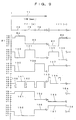
explained using FIG. 9. FIG. 9 is a chart of driving waveforms used in a
liquid crystal display device in this embodiment.
It should be noted that the liquid crystal display device used in the
fourth embodiment is also the same as that explained in the first embodiment,
and thus the description thereof is omitted.
Further, upper four signals showing a color display signal in the
waveform chart in FIG. 9 are the same as those explained in the third
embodiment using FIG. 8, and thus the description thereof is also omitted.
What is explained in this embodiment is a low power driving signal
having both characteristics of a limited color display pattern signal for
applying selection signals only to part of signal electrodes and a color
reducing display signal for simultaneously selecting a plurality of signal
electrodes.
In this embodiment, the driving voltage of a low power display is
composed of six levels of V1, V2, V3, V4, V5 and V6 as in the case of the
color display signal.
To a first signal electrode, a low power eleventh selection signal 151
at V6 voltage level is applied during a period corresponding to a first
selection period 74 and a second selection period 75 in Tf1(+), and a low
power eleventh non-selection signal 152 at V2 voltage level is applied during
the other periods in Tf1(+). The same signal as that applied to the first
signal electrode is also applied to a second signal electrode. No selection
signal is applied to a third signal electrode. As for the other signal
electrodes, for example, low power selection signals are applied to fourth and
fifth signal electrodes during the same periods, and no selection signal is
applied to a sixth electrode. In such a manner, low power selection signals
are applied to two out of three electrodes in every group and not to the
remaining one. The low power selection signals are, of course, applied in a
time sharing manner to every group of two signal electrodes.
A low power twelfth selection signal 153 at V1 voltage level is
applied to the first signal electrode during a period corresponding to the first
selection period and the second selection period in Tf1(-). A low power
twelfth non-selection signal 154 at V5 voltage level is applied during the
other periods in Tf1(-). A signal which is the same as that of the first signal
electrode is also applied to the second signal electrode. No selection signal
is applied to the third signal electrode. Selection signals of Tf1(-) are also
applied to the other signal electrodes in the time sharing manner as in the case
of Tf1(+).
Next, a low power data signal which is applied to a data electrode will
be explained. The driving voltage of the low power data signal is also
composed of six levels of V1, V2, V3, V4, V5 and V6.
The same low power eighth data signal 155 at V1 voltage level is
applied to the first data electrode during the first selection period 74 and the
second selection period 75. A low power ninth data signal 156 at V4 voltage
level is applied during the third selection period 76. A low power data
signal at V1 (bright) or V4 (dark) voltage level is applied during the other
periods in accordance with the display contents of other groups of three signal
electrodes.
A low power tenth data signal 157 at V6 voltage level or a low power
eleventh data signal 158 at V3 voltage level is applied during the periods in
Tf1(-) in accordance with the display contents.
Accordingly, the case which is described here provides a display in
which a pixel of yellow made by mixing red and green turns ON/OFF.
As is clear from the above explanation, the selection period of the
signal electrode in the low power display is twice as long as that in the state in
which a 512-color display is performed. Further, the voltage application
period of the data signal is also twice as long. Therefore, the driving voltage
can be reduced. Furthermore, the division into the 1st-part gradation signal
and the 2nd-part gradation signal is stopped, and a binary display is provided
using all the periods. Accordingly, the switching of the voltage of the signal
electrode is reduced to half because the selection period is twice as long.
The switching of the voltage of the data electrode is similarly reduced to half.
Consequently, the power consumption can be reduced to half or less.
Further, the driving voltage can be reduced.
Moreover, the selection period for application to the signal electrode
is increased, thereby reducing the driving frequency. Further, a plurality of
signal electrodes are simultaneously selected to make the display as bright as
possible and to add color information, thereby improving visibility.
Furthermore, display colors can be changed by changing electrodes to which
selection signals are applied, so that colors are changed in accordance with
use environments to enable realization of both securement of visibility and
low power consumption. Further, the number of gradations of voltage
applied to the data electrodes is reduced to thereby simplify its driving circuit,
making it possible to reduce the power consumption.
Although two out of three signal electrodes are selected here, it is also
suitable to select one signal electrode. Further, it is also possible to divide
the low power data signal into a 1st-part gradation signal and a 2nd-part
gradation signal to perform the gradation display.
Fifth embodiment
Next, the fifth embodiment of the present invention will be explained
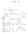
using FIG. 10. FIG. 10 is a chart of driving waveforms used in a liquid
crystal display device in this embodiment.
It should be noted that the liquid crystal display device used in the
fifth embodiment is also the same as that explained in the first embodiment,
and thus the description thereof is omitted.
Further, upper two signals showing a full color display signal in the
waveform chart in FIG. 10 are the same as those explained in the first
embodiment using FIG. 6, and thus the description thereof is also omitted.
What is explained in this embodiment is a reduced color display
pattern signal for performing a reduced color display in which R, G, B filters
can be selected with their gradation individually reduced.
In this embodiment, the driving voltage of a low power display is
composed of six levels of V1, V2, V3, V4, V5 and V6 as in the case of the
full color display signal. As in the case of the full color display, a selection
signal at V6 voltage level is applied to each signal electrode during a selection
period corresponding to each signal electrode in Tf1(+), and a non-selection
signal at V2 voltage level is applied during the other periods in Tf1(+). A
selection signal at V1 voltage level is applied during a selection period
corresponding to each signal electrode in Tf1(-), and a non-selection signal at
V5 voltage level is applied during the other periods in Tf1(-).
Next, a low power data signal which is applied to a data electrode will
be explained. The driving voltage of the low power data signal is also
composed of six levels of V1, V2, V3, V4, V5 and V6.
The low power data signal for each pixel portion in this embodiment,
different from the data signal for the full color display, is not divided into a
1st-part gradation signal and a 2nd-part gradation signal, and is made a binary
data signal only with ON/OFF.
In the example shown in the drawing, a low power tenth data signal
270 at V1 voltage level is applied to a first data electrode during the first
selection period 74 and the third selection period 76 in Tf1(+), and a low
power eleventh data signal 271 at V4 voltage level is applied during the
second selection period 75. A low power data signal at V1 (bright) or V4
(dark) voltage level is applied during the other periods in accordance with the
display contents of other signal electrodes.
A low power twelfth data signal 272 at V6 voltage level (bright) or a
low power thirteenth data signal 273 at V3 voltage level (dark) is applied
during the periods in Tf1(-) in accordance with the display contents of the
signal electrode.
The arrangement of R, G, B color filters 3 respectively at the first,
second and third signal electrodes provides a display in a color of magenta
made by mixing red and blue in the case described here.
As is clear from the above explanation, the number of gradations of
the voltage applied to the data signal is reduced in the reduced color display
as compared with the state in which a 512-color display is performed to
thereby simplify its driving circuit, making it possible to reduce the power
consumption.
The data signal is made binary of ON/OFF here, but the data signal at
eight gradations is made to be at four gradations, thereby also providing effect
of reducing power consumption.
Sixth embodiment
Next, the sixth embodiment of the present invention will be explained
using FIG. 6, FIG. 11 and FIG. 12. FIG. 11 is a plan view, similar to FIG. 4,
of a liquid crystal display device to which this embodiment is applied. FIG.
12 is a sectional view along a line 12-12 in FIG. 11.
In this liquid crystal display device used in the sixth embodiment, red
(R) color filters 33, green (G) color filters 34 and blue (B) color filters 35 in
the form of stripes are provided parallel to data electrodes 5 as shown in FIG.
11 and FIG. 12. This liquid crystal display device is different only in this
point from the liquid crystal display device which is described in the first
embodiment, and thus the description of the other points is omitted.
This liquid crystal display device can individually control the
gradations of pixels of R, G, B even if the color display signal which is
explained in the first embodiment using FIG. 6 is applied thereto, therefore
performing a 512-color display which is the full color display and the normal
color display which are the same as those of the first embodiment.
This embodiment is characterized in that a color display can be
performed even if the reduced color display signal shown in FIG. 6 is used for
performing the display.
In this liquid crystal display device, the same low power selection
signals composed of a low power first selection signal 100, a low power non-selection
signal 101 and the like are applied to a first through a third signal
electrode to simultaneously select them, not leading to the integral selection
of three color filters as distinct from the case of the first embodiment.
Low power data signals are applied to the data signals one by one to
individually select respective pixels of R, G, B, thereby performing the
normal color display. Particularly when a gradation display is performed
using a low power first 1st-part gradation signal 108 and a low power first
2nd-part gradation signal 109, a full color display can be performed in which
the pixels of R, G, B are selected with gradations respectively. In other
words, a color display at the same level as that by the color display signal can
be performed using the reduced color display signal.
On the other hand, the applied signal is the same as that which is
explained in the first embodiment, and thus the low power effect as is
explained in the first embodiment can be obtained. Accordingly, the color
display with reduced power consumption can be performed in this
embodiment.
However, since three signal electrodes are simultaneously selected,
the display contents are stretched three times as long as that of the display by
the color display signal in a direction in which the signal electrodes are
arranged. Therefore, a figure such as a circle or the like is low in accuracy,
but a display of character or number can be sufficiently recognized and
effective.
Further, by applying the same low power data signals to every group
of nine data electrodes (three groups of R, G, B), the display contents are
stretched three times as long respectively in directions in which the signal
electrodes and data electrodes are arranged, thereby performing a display, a
black-and-white display, having the same aspect ratio as that of the display by
the color display signal.
Furthermore, the data electrodes are made into groups in threes
composed of R, G, B, and the same low power data signals are applied to R
and G, and a signal for always providing black is applied to B, thereby also
enabling the limited color display of performing a display in yellow and black.
Similarly, it is also possible to apply the same low power data signals to R
and B or G and B.
The number of the data electrodes to which the low power data signals
are applied is selected to thereby change the number of feasible colors as
described above, achieving reduced power consumption. Therefore, it is
extremely effective to employ the color reducing display pattern signal to a
liquid crystal display device having a liquid crystal display panel with a
structure in which color filters are disposed on the data electrodes.
Although the example in which three signal electrodes are
simultaneously selected is shown here, the number of the signal electrodes
simultaneously selected may be any number which is two or more. The
greater number of the signal electrodes are simultaneously selected, the
greater the effect of reducing power consumption is. The display, however,
is correspondingly stretched in the direction in which the signal electrodes are
arranged, lowering the display quality, and thus it is suitable to determine the
number of the signal electrodes simultaneously selected in accordance with
uses when necessary.
Seventh embodiment
Next, the seventh embodiment of the present invention will be
explained with reference to FIG. 13 to FIG. 16.
FIG. 13 is a planar schematic view of a timepiece including a liquid
crystal display panel to which the seventh embodiment of the present
invention is applied. FIG. 14 is a sectional view of the timepiece along a
line 14-14. FIG. 15 is a plan view showing the liquid crystal display panel
used in the timepiece. FIG. 16 is a partially enlarged view of FIG. 15.
The timepiece including the liquid crystal display panel to which the
seventh embodiment is applied will be explained first.
This timepiece is, as shown in FIG. 13, an analog timepiece for
displaying the time with a minute hand 46, an hour hand 47 and hour numbers
60, and has a liquid crystal display panel including a display region 13 over
an entire region inside a panel cover 163, so that various kinds of information
can be displayed on the liquid crystal display panel. Further, the timepiece
has an adjusting button 162 for turning ON/OFF a display of the liquid crystal
display panel, changing the display contents, correcting the time, and turning
on a light source.
FIG. 13 shows the state in which the upper side of the display region
13 of the timepiece is made a full color display region for performing a full
color display in 512 colors, while a low power display region 53 on the lower
side is operated in a low power mode to perform a monochrome display,
thereby reducing the electric power consumed by the liquid crystal display
device. A low power mode display 55 showing this state is further displayed.
The liquid crystal display panel in this timepiece is constituted by
providing, from the opposite side to a cover glass 58 (the back side) as shown
in FIG. 14, a first substrate 1 and a second substrate 4 which is opposed to the
first substrate 1 with a predetermined gap interposed therebetween. Signal
electrodes, opposed electrodes, color filters and the like are omitted in FIG.
14, and thus they are described later.
A liquid crystal layer 43 is provided between the first substrate 1 and
the second substrate 4, and the liquid crystal layer 43 is sealed with a sealing
material 9 and a not shown closing material. Further, alignment films (not
shown) made of a polyimide resin are provided on the first substrate 1 and the
second substrate 4 respectively to align the liquid crystal layer 43 in
predetermined directions. In this embodiment, a twisted nematic liquid
crystal is used as the liquid crystal layer 43, and is aligned in a direction of
7:30 on the first substrate 1 and in a direction of 4:30 on the second substrate
4, thereby making a twist angle of the liquid crystal layer 43 to be 90°.
However, what is used as the liquid crystal layer 43 is not limited to the
twisted nematic liquid crystal, but another liquid crystal, for example, a guest
host-type liquid crystal, a scattering-type liquid crystal, a selective reflection-type
liquid crystal or the like may be applicable.
A first polarizing film 21 composed of RDF (trade name)
manufactured by 3M Ltd. is provided on the first substrate 1 as a reflection-type
polarizing film. A second polarizing film 22 composed of an
absorption-type polarizing film in which pigment is stretched in one direction
is provided on the second substrate 4. The first polarizing film 21 and the
second polarizing film 22 are arranged so that transmission axes thereof are
perpendicular to each other to be brought into a state of exhibiting strong
reflection characteristics when a voltage applied to the liquid crystal layer 43
is large, and exhibiting transmission characteristics when the applied voltage
is small by combination with the liquid crystal display panel. This
constitutes the liquid crystal display panel.
Further, in this timepiece, a light source 66 is disposed on the back
side of the liquid crystal display panel to allow the timepiece to be usable in a
dark environment, and a circuit board 68 is disposed on the back side of the
light source 66 as shown in FIG. 14. The liquid crystal display panel is
connected to the circuit board 68 with a zebra-rubber connector 61, and the
light source 66 is connected to the circuit board 68 through a light source
terminal 67. The zebra-rubber connector is used as the light source terminal
67, but a spring may be used.
A battery 64 is fixed to the circuit board 68. This battery 64 is an
energy source of this timepiece. A driver 69 having a hand shaft 48 linked
to the minute hand 46 and the hour hand 47 is disposed between the light
source 66 and the circuit board 68. The hand shaft 48 projects from the
driver 69 through a hand shaft hole 49 including an opening portion 54 of the
liquid crystal display panel into the cover glass 58 side.
Further, a printing layer 50 having a shielding effect is provided and
the hour characters 60 are formed on the cover glass 58 side of the first
polarizing film 21. Furthermore, a module frame 70 has the panel cover 163.
The timepiece module structured as above is installed within a case 161, the
cover glass 58 and a case back 57, thereby constituting the timepiece to which
this embodiment is applied.
Next, the structure of the liquid crystal display panel will be explained
in more detail. As shown in FIG. 15 and FIG. 16, signal electrodes 2
composed of a transparent conductive film are provided on the first substrate
1 composed of a transparent substrate. The signal electrodes 2 are in a
column electrode pattern in which a first signal electrode 2-1 to an n-th signal
electrode 2-n are in the form of almost parallel stripes except for a detouring
portion 80 around the opening portion 54 in the display region 13. The
signal electrode around the opening portion 54, as represented by an m-th
signal electrode 2-m, is formed therein with the signal electrode detouring
portion 80 which is thinner in width than that of the signal electrode 2 in the
stripe form so as to detour the opening portion.
Further, data electrodes 5 composed of a transparent conductive film
are provided on the second substrate 4 which is opposed to the first substrate
1 with a predetermined gap interposed therebetween. The data electrodes 5
are in a row electrode pattern in which a first data electrode 5-1 to a q-th data
electrode 5-q are in the form of stripes in the display region 13. As the data
electrode 5 in one row, two electrodes are formed from the top and the bottom
with ends at the center respectively. The data electrode 5 in the vicinity of
the opening portion 54 has a length shorter than that of the other data
electrodes 5 and has a shape which ends in the vicinity of the opening portion
54 due to the outline of the liquid crystal display panel.
The signal electrodes 2 provided on the first substrate 1 are connected
to connecting electrodes 44 on the second substrate 4 by forming the sealing
material 9 out of an anisotropic conductive sealing material, which is
provided around the display region and used for sealing the liquid crystal
layer 43. The connecting electrodes 44 are alternately formed on the right
and the left at every other electrode. The anisotropic conductive sealing
material, in which conductive particles (not shown) are mixed in an insulating
resin, can connect the signal electrode 2 to the connecting electrode 44
through the conductive particles. The same numbers of the connecting
electrodes 44 are led to this side and the backside of the display region 13 in
the drawing to enable the connection to the circuit board. This is an
effective structure when the number of pixel portions is small because its
display region can occupy a large area with respect to the outline of the
substrate.
As shown in FIG. 16, red (R) color filters 33, green (G) color filters
34 and blue (B) color filters 35 are provided on the second substrate 4. Each
color filter is in stripe form. In this liquid crystal display device, the color
filters 33, 34 and 35 are in the form of stripes parallel to the signal electrodes
2. Thus, a sharp display can be attained when using a color reducing display
pattern signal, a limited color display pattern signal, or a reduced color
display pattern signal.
It should be noted that the color filters 3 may be composed of three
colors of cyan (C), magenta (M) and yellow (Y), or may be color filters in the
form of dots.
The data electrodes 5 are provided on the color filters 33, 34 and 35
through an interlayer insulation film (not shown) made of an acrylic resin.
As shown in FIG. 16, a portion where the signal electrode 2 and the data
electrode 5 overlap one another forms a pixel portion 7, and a region where a
plurality of the pixel portions 7 are arranged in a matrix form is the display
region 13.
The display control of the timepiece including the liquid crystal
display panel as described above is conducted by driving it by the driving
signals explained in the first to fifth embodiments and switching when
necessary between the full color display and the display by low power
consumption of the color reducing display, the limited color display or the
reduced color display, thereby reducing the power consumption and
performing the dot matrix-type color display in the timepiece.
Eighth embodiment
Next, the eighth embodiment of the present invention will be
explained with reference to FIG. 17 to FIG. 21.
FIG. 17 is a planar schematic view of a timepiece having a liquid
crystal display panel to which the eighth embodiment of the present invention
is applied. FIG. 18 is a plan view showing the liquid crystal display panel
used in the timepiece. FIG. 19 is a sectional view of the timepiece along a
line 19-19. FIG. 20 is a block diagram showing circuits for reducing the
power consumption of the timepiece. FIG. 21 is a view showing examples
of the control of reducing power consumption conducted with a dot matrix
display portion of the timepiece divided into the top and the bottom.
The timepiece including the liquid crystal display panel to which the
eighth embodiment applies will be explained first.
This timepiece, as shown in FIG. 17, is a timepiece for showing the
time in a digital display on a time display portion 173, and further includes a
character display portion 170, a schedule display portion 171 and a menu
display portion 172, and thus it is a timepiece capable of displaying various
information in addition to the time. Further, this timepiece includes an
adjusting button 162 for changing the display contents and a switch 222 for
switching its display mode.
A liquid crystal display panel 20 provided in this timepiece is
provided with a first substrate 1 and signal electrodes in order from the
opposite side to a cover glass 58 (the back side). Two types of signal
electrodes are provided, which are in the form of stripes and in the form of
segments. Red (R) color filters, green (G) color filters and blue (B) color
filters are provided on the second substrate 4 which is opposed to the first
substrate 1 with a predetermined gap interposed therebetween. In this liquid
crystal display device 20, the color filters are in the form of stripes parallel to
the data electrodes. More specifically, the color filters are provided in the
region where they overlap the data electrodes in the form of stripes described
later, and not in a portion over the data electrodes in the form of segments.
By virtue of the form of stripes parallel to the data electrodes, a sharp display
can be attained when using a color reducing display pattern signal, a limited
color display pattern signal, or a reduced color display pattern signal.
It should be noted that the color filters may be composed of three
color filters of cyan (C), magenta (M) and yellow (Y), or may be color filters
in the form of dots.
An interlayer insulation film made of an acrylic resin is provided on
the color filter. The data electrodes in the form of stripes and the data
electrodes in the form of segments are provided on the interlayer insulation
film. A portion where the signal electrode and the data electrode overlap
one another forms a pixel portion. A region where a plurality of the signal
electrodes in the form of stripes overlap the data electrodes is a dot matrix
display region 181 shown in FIG. 18, and a region where the signal electrodes
in the form of segments overlap the data electrodes is a segment display
region 182.
The dot matrix display region 181 shown in FIG. 18 constitutes the
character display portion 170 and the schedule display portion 171. The
character display portion 170 and the schedule display portion 171 are not
necessarily in the positional relation like this, but are set in any positions in
the dot matrix display portion 181 when necessary.
The segment display region 182 constitutes the menu display portion
172 and the time display portion 173. The time and the menu are made the
segment type and the display region with much information is made the
matrix type, thereby reducing the power consumption. It should be noted
that no color filter is provided over the time display portion 173, giving a
priority to brightness and a reduction in power consumption, providing a
monochrome display. Further, a full color display, a reduced color display, a
color reducing display, and a limited color display which include gradation
signals are used in the dot matrix display portion 181, thereby enabling
various types of displays from a display of high quality to one in the low
power mode.
As shown in FIG. 19, a liquid crystal layer 43 is provided between a
first substrate 1 and a second substrate 4, and the liquid crystal layer 43 is
sealed with a sealing material 9 and a closing material 10. Further,
alignment films (not shown) made of a polyimide resin are provided on faces
on the liquid crystal layer 43 side of the first substrate 1 and the second
substrate 4 to align the liquid crystal layer 43 in predetermined directions.
When a super twisted nematic (STN) liquid crystal is used as the liquid
crystal layer 43, any twist angle ranging from 210 degrees to 260 degrees is
employed as the twist angle of the liquid crystal layer 43. However, another
liquid crystal, for example, a guest host-type liquid crystal, a scattering-type
liquid crystal, a selective reflection-type liquid crystal or the like may be used
for the liquid crystal layer 43.
A first polarizing film 21 composed of RDF (trade name)
manufactured by 3M Ltd. is provided on the face opposite to the liquid crystal
layer 43 of the first substrate 1 as a reflection-type polarizing film. A second
polarizing film 22 composed of an absorption-type polarizing film in which
pigment is stretched in one direction is provided on the face opposite to the
liquid crystal layer of the second substrate 4. The first polarizing film 21
and the second polarizing film 22 are arranged so that transmission axes
thereof are parallel to each other to be brought into a state of exhibiting strong
reflection characteristics when a voltage applied to the liquid crystal layer 43
is small, and exhibiting transmission characteristics when the applied voltage
is large by combination with the liquid crystal display panel 20. This
constitutes the liquid crystal display panel 20.
A light source 66 is disposed on the back side of the liquid crystal
display panel 20 to allow the timepiece to be usable in a dark environment,
and a circuit board 68 is disposed on the back side of the light source. A
battery 64 is fixed to the circuit board 68. On the opposite side to the visible
side of the second substrate 4, an LCD controller and driver IC (integrated
circuit) 178 for applying predetermined signals to the signal electrodes and
data electrodes is implemented by a chip-on-glass mounting method (a face
down bonding method) as shown in FIG. 18. The signal electrodes and data
electrodes of the dot matrix display portion 181 and the segment display
portion 182 are connected to the LCD controller and driver IC 178 via
connecting electrodes including signal electrode connecting electrodes though
the illustration thereof is omitted, so that they are driven by applied voltage
(signal) supplied from the LCD controller and driver IC 178.
In order to allow the number of ICs mounted to be one, signal
electrodes 175 in the form of stripes are electrically arrangement-changed to
the signal electrode connecting electrodes which are provided on the second
substrate 4 using an anisotropic conductive adhesive in which conductive
particles are dispersed in the sealing material 9. The signal electrodes in the
form of segments are also arrangement-changed onto the second substrate 4
similarly using the anisotropic conductive adhesive.
External signals are inputted into the LCD controller and driver IC
178 via input electrodes 180 which are provided on the second substrate 4,
and a zebra rubber connector 61 connects the circuit board 68 and the input
electrodes 180.
A liquid crystal module composed of the liquid crystal display panel
20 with the LCD controller and driver IC 178 mounted, the circuit board 68,
the light source 66 and a holding frame 210 is set in a watch case 161,
constituting a timepiece. A panel cover 163 is provided in the timepiece to
shield a part of the liquid crystal module which is unnecessary to be seen,
thereby preventing the unnecessary part from being watched by a user of the
timepiece.
Further, a power generating function is provided to the timepiece to
enable the timepiece to be used for a long time without replacement of the
battery 64. In this timepiece, a case back 57 is made of a material
transmitting light, and a solar cell 205 is provided as a power generator inside
the case back 57 through an ultraviolet cut film 206. Further, the panel
cover is a solar cell 204. The solar cells 204 and 205 are connected to the
circuit board 68 via connecting wires 208 and 207 respectively.
The battery 64 is charged by the solar cell 204 which is the panel
cover in a normal use condition of the timepiece, and it is charged by the solar
cell 205 which is provided on the case back 57 when the timepiece is not
carried. The solar cells are arranged as above, thereby obtaining a sufficient
quantity of power generation while keeping the display region of the liquid
crystal display panel 20 wide.
In addition to the solar cell, a mechanism for converting the kinetic
energy into the electric energy, a mechanism for converting the heat energy to
the electric energy or the like may be used as the power generator.
Next, the configuration of circuits which realizes the low power
display of this timepiece will be explained.
As shown in FIG. 20, the power generating states of the solar cells
204 and 205 which are power generators 185 are detected by a voltage
detection circuit 186. The generated energy by the solar cells is sent from
the voltage detection circuit 186 through a charging voltage conversion circuit
188 and accumulated in a secondary battery 187. A battery remaining
capacity detection circuit 189 detects the states of the voltage detection circuit
186 and the secondary battery 187 and sends them out to a display mode
switching signal generation circuit 194.
The display mode switching signal generation circuit 194 sends out a
signal for selecting a gradation signal generation circuit 196, a full color
display pattern signal generation circuit 197, a reduced color display pattern
signal generation circuit 198, a color reducing display pattern signal
generation circuit 199, a limited color display pattern signal generation circuit
200 and a display stop circuit 201 included in a plural simultaneous selection
circuit block 195 in accordance with information from the battery remaining
capacity detection circuit 189, that is, the battery remaining capacity and the
quantity of power generation.
The full color display pattern signal generation circuit 197, the
reduced color display pattern signal generation circuit 198, the color reducing
display pattern signal generation circuit 199, and the limited color display
pattern signal generation circuit 200 are circuits for generating the full color
display pattern signal, the reduced color display pattern signal, the color
reducing display pattern signal, and the limited color display pattern signal
respectively which are explained in the above embodiments. It is possible to
simultaneously select a plurality of the circuits 198 to 200 to generate a
display signal having characteristics of a plurality of display pattern signals.
The display stop circuit 201 is a circuit for stopping the display of the dot
matrix display portion 181.
The gradation signal generation circuit 196 is a circuit for giving a
gradation to the signal generated by each of the circuits 197 to 200, and is
selected separately from the circuits 197 to 201. When the gradation signal
generation circuit 196 is not selected, the gradation display is not performed,
but the power consumption can be reduced.
The display mode switching signal generation circuit 194 selects a
circuit which performs a display requiring less power consumption when the
remaining capacity of the battery is in decreased state, and selects the display
stop circuit 201 when the quantity decreases to less than a certain limit to stop
the display of the dot matrix display portion 181. However, what are
selected in the plural simultaneous selection circuit block 195 are only the
circuits for the display of the dot matrix display portion 181, and the display
of the segment display portion 182 is always performed constant regardless of
the selection.
In this embodiment, the dot matrix display portion 181 is controlled
divided into an upper display region 212 and a lower display region 213 as
shown in FIG. 21, and thus circuits are separately selected for these.
However, the entire dot matrix display portion 181 may be controlled as one
display region.
In order to successively apply signals to the signal electrodes or the
data electrodes of the liquid crystal display panel 20 constituting the
timepiece, a signal generated by a reference clock oscillation circuit 190 is
divided to a vertical synchronizing circuit 192 and a horizontal synchronizing
circuit 193 through a synchronization separation circuit 191.
In the plural simultaneous selection circuit block 195, data to be sent
out to a selection signal generation circuit 202 and a data signal generation
circuit 203 is generated based on data from a display data generation circuit
described later and output signals by the vertical synchronizing circuit 192
and the horizontal synchronizing circuit 193. Then, a selection signal
generated in the selection signal generation circuit 202 and a data signal
generated in the data signal generation circuit 203 based on the data are
applied to the liquid crystal display panel 20.
The display data except for the time is generated by a display data
except-for-time generation circuit 221 and inputted into the plural
simultaneous selection circuit block 195.
As for the time display data, time is measured in a time count circuit
183 by an output clock of the reference clock oscillation circuit 190, and time
display data is generated in a time display data generation circuit 184 based
on the time measured in the time count circuit 183, and inputted into the
plural simultaneous selection circuit block 195.
The display method of the dot matrix display portion 181 may be
selected with a switch 222. In this case, the information of the switch 222
being pushed is transmitted to the plural simultaneous selection circuit block
195, and circuits are selected in accordance with the information.
Further, the display method of the dot matrix display portion 181 can
be changed after every lapse of fixed time. In this case, a timer 220 for
measuring time by the output clock of the reference clock oscillation circuit
190 sends out a signal to the plural simultaneous selection circuit block 195 at
a previously determined point of time, and circuits are selected in accordance
with the signal.
The low power display is controlled with the dot matrix display
portion 181 of this timepiece divided into two display regions as described
above. An example of this control is explained below.
FIG. 21 shows display modes 215 to 218 for the dot matrix display
portion 181. In 215, both the upper display region 212 and the lower display
region 213 perform the full color display in 512 colors. In other words, this
is a display by a maximum display ability of the liquid crystal display panel
20 of this timepiece with high power consumption of the liquid crystal display
device.
In 216, the upper display region 212 performs the full color display,
but the lower display region 213 performs the reduced color display in which
the number of gradations is reduced using the reduced color display pattern
signal to thereby reduce the number of colors to eight in order to reduce the
power consumption.
In 217, the same color reducing display pattern signal is applied to
every group of three signal electrodes and only the data electrode for one
color out of three data electrodes for R, G, B in every group is used in the
upper display region 212, thereby limiting the number of display colors to
four. The same color reducing pattern signal is applied to every group of
three signal electrodes and every group of three data electrodes, and further,
gradation display is not performed, resulting in the black-and-white binary
display in the lower display region 213, thereby efficiently reducing the
power consumption. In this embodiment, the color filters are formed
parallel to the data electrodes, and thus when the color reducing display
pattern signal is used which simultaneously selects a plurality of the signal
electrodes, the display is vertically stretched as compared with that of the full
color display.
In 218, the same color reducing pattern signal is applied to every
group of three signal electrodes and every group of three data electrodes, and
further, gradation display is not performed, resulting in the black-and-white
binary display gradation display in the upper display region 212 to thereby
efficiently reduce the power consumption, and the limited color display
pattern signal for driving two signal electrodes and stopping one is applied in
the lower display region 213. Further, the color reducing display pattern
signal is integrally used to thereby increase the size of a character, thereby
decreasing influence which is exerted upon the visibility due to the stop of
driving of the signal electrodes.
The power consumption is reduced from 215 to 216, 217, 218 when it
can not be expected to obtain an electric power enough for driving because of
a decrease in the remaining capacity of the secondary battery 187 which is an
energy source of the liquid crystal display device or a decrease in the quantity
of power generation by the solar cell 204 which is the power generator 185,
when a user of the timepiece pushes the switch 222, or when a previously set
time is elapsed.
When the remaining capacity of the secondary battery 187 recovers or
the quantity of power generation by the solar cell 204 recovers to secure
sufficient electric power, or when the user of the timepiece operates it, the
display is returned to 215, releasing the reduction in power consumption.
The example shown here is just an example of the control of reducing
the power consumption, and the order or the combination of display pattern
signals in use is not limited to this.
The example in which the dot matrix display portion 181 is always
controlled with divided into the upper display portion 212 and the lower
display portion 213 is shown here, but it is also suitable to control it shifting
its boundary line or dividing it into three or more regions in accordance with
the circumstances.
Further, the example in which the liquid crystal display panel 20
provided with the color filters which are parallel to the data electrodes 5 is
described here, and the same control can also apply to one provided with the
color filters which are parallel to the signal electrodes 2.
According to the method capable of driving the liquid crystal display
panel in the low power mode as described above, the power consumption can
be reduced and the dot matrix type color display can be performed in the
timepiece. 'Further, the employment of the low power mode enables a
function as a timepiece to be maintained with a power generating mechanism
in a size installable in the timepiece. Furthermore, the low power mode of
the liquid crystal display panel is switched in accordance with the remaining
capacity of the battery, making it possible to increase the battery life. Two
types of power generating mechanisms are employed to switch between the
method of charging during the wearing of the timepiece and that during the
non-wearing of it, thereby enabling the charge without decreasing the display
quality of the liquid crystal display panel.
Further, the use of a signal having characteristics of two or more out
of the reduced color display pattern signal, the color reducing display pattern
signal and the limited color display pattern signal can further reduce the
power consumption.
Incidentally, this embodiment describes the timepiece including the
liquid crystal display panel, but it is, of course, possible to drive a liquid
crystal display panel of another liquid crystal display device using the same
control circuit.
INDUSTRIAL APPLICABILITY
As has been described, according to a method of driving a liquid
crystal display panel of the present invention, a color reducing display is
performed using a color reducing display pattern signal of simultaneously
selecting a plurality of signal electrodes, thereby making it possible to
increase the period of time in which the signal electrodes are selected as
compared with that of a color display pattern signal. In other words, the
frequencies of selection signal and data signal can be decreased.
Further, as a liquid crystal layer electro-optically changes by an
effective voltage which is applied thereto during a fixed period, a plurality of
the signal electrodes are simultaneously selected to reduce the number of time
sharing, making it possible to reduce the voltages of the selection signal and
the data signal according to a voltage averaging method. The reduction in
the frequency and the reduction in the voltage enable reduction in the electric
power consumed by the liquid crystal display device in both its driving circuit
and liquid crystal layer. Additionally, the selection of the plurality of the
selection signals results in the simultaneous selection of a plurality of color
filters, enabling a bright display.
It is extremely effective to apply this color reducing display to a liquid
crystal display device having color filters in the form of stripes parallel to the
data electrodes, thereby reducing the power consumption while maintaining a
display in the same number of colors as that of the color display pattern signal.
Further, a limited color display is performed using a limited color
display pattern signal of selecting only part of the signal electrodes, also
making it possible to increase the period of time in which the signal
electrodes are selected as compared with the color display pattern signal and
to decrease the frequencies of the selection signal and the data signal.
Furthermore, the signal electrodes to be selected are changed in accordance
with circumstances or objects to thereby change colors in this case, enabling
realization of both securement of visibility and low power consumption.
Further, a reduced color display is performed using a reduced color
display pattern signal in which the number of gradations of the data signal is
reduced than that in the case of a full color display, thereby simplifying the
driving of the driving circuit of the data signal, enabling low power
consumption.
Moreover, further reduction in power consumption can be achieved by
performing a display using a signal having combined characteristics of these
signals.
The display of the liquid crystal display panel is switched into a
display by low power in accordance with the remaining capacity of the battery,
the quantity of power generation or the operation by a user, thereby realizing
low power consumption while suppressing the decrease in the display quality
to the minimum, and increasing battery life when it is driven by a battery.
The effects are further prominent when a display region of the liquid crystal
display panel is divided into a plurality of regions and they are controlled
individually.
Accordingly, the method of the present invention applies to display
control of a timepiece, thereby enabling a color display by the liquid crystal
display panel also in the timepiece to which reduction in power consumption
is strongly required from the viewpoints of shape and size.
The present invention can be applied not only to the timepiece, but
also to liquid crystal display panels of electronic devices such as a personal
digital assistants, a portable information terminal, a cellular phone, a mobile
game machine and the like, thereby reducing the power consumption of these
electronic devices to provide electronic devices friendly to the earth
environment.