EP1148441A1 - Circuit condenseur de distribution d'activité - Google Patents
Circuit condenseur de distribution d'activité Download PDFInfo
- Publication number
- EP1148441A1 EP1148441A1 EP00810333A EP00810333A EP1148441A1 EP 1148441 A1 EP1148441 A1 EP 1148441A1 EP 00810333 A EP00810333 A EP 00810333A EP 00810333 A EP00810333 A EP 00810333A EP 1148441 A1 EP1148441 A1 EP 1148441A1
- Authority
- EP
- European Patent Office
- Prior art keywords
- moments
- input
- network
- circuit
- nodes
- Prior art date
- Legal status (The legal status is an assumption and is not a legal conclusion. Google has not performed a legal analysis and makes no representation as to the accuracy of the status listed.)
- Withdrawn
Links
Images


Classifications
-
- G—PHYSICS
- G06—COMPUTING OR CALCULATING; COUNTING
- G06N—COMPUTING ARRANGEMENTS BASED ON SPECIFIC COMPUTATIONAL MODELS
- G06N3/00—Computing arrangements based on biological models
- G06N3/02—Neural networks
- G06N3/06—Physical realisation, i.e. hardware implementation of neural networks, neurons or parts of neurons
- G06N3/063—Physical realisation, i.e. hardware implementation of neural networks, neurons or parts of neurons using electronic means
- G06N3/065—Analogue means
Definitions
- the present invention relates to a condenser circuit of activity distribution, i.e. a circuit capable of determining precisely the "center of gravity" of an activity, represented by analog quantities, distributed on a plurality of nodes of a network.
- the initial information is present under the form of analog quantities distributed over a network of nodes defining a space. This is the case, in particular, of a array, for example one-dimensional, of photodiodes which are subject to any kind of illumination.
- a photodiodes activity center - that is, the position of the point (activity center) where an activity could be concentrated global - to significantly represent the activity distributed.
- the activity in an artificial retina, is the intensity generated in the points (or pixels) of the retina by light reaching that same retina.
- activated points or activity center
- the possibility of ability to focus activity on one or two points, rather than on all the points of an image can be very advantageous in terms of the amount of information to be processed locally or forward to subsequent processing stages.
- an activity distribution condenser circuit is still very useful for re-focusing the spot between networks.
- center of gravity used here is borrowed from mechanics because, as we will see later, a analogy can be made between the operating principles of the circuit of the invention and the calculation of the moments of forces with respect to to a center of gravity.
- the object of the present invention is a concentration circuit which, from an activity distribution represented as analog quantities present on the nodes of a network input, provides output information on two nodes adjacent output so that said adjacent nodes of exit frame the center of gravity of said activity distribution and that, on each of said adjacent output nodes, either has an analog output quantity; the report of said two analog output quantities indicating the distance of said center of gravity at each of said adjacent output nodes.
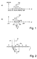
- the diagram of FIG. 1 represents in a) a distribution of activity over a given number of preferential positions or input nodes (p0 to p8).
- the activities are represented in the form of vertical bars whose heights are representative of the activities on the respective nodes. As indicated previously, these activities can correspond to the intensities generated by the diodes of a network of photodiodes and the preferential positions correspond to the positions of the photodiodes in said network.
- the activity center CA that is to say the point on the network where all the activity could be concentrated, is located between the positions p4 and p5 at a point closer to p4 than to p5.
- FIG. 2 representing a beam (of mass assumed to be zero) subjected to forces F1 to F3 distributed over a certain number of points (1, 2 and 3).
- the present invention proposes to exploit this analogy as described in relation to FIG. 3.
- FIG. 3.a a distribution of input activity distributed over a finite number of input nodes. (p0 to p5).
- it is proposed to carry out for each node the sum of the "moments", that is to say the sum of the products of the activity of the other nodes by the distance which separate them from the chosen node.
- Figure 1.b shows, for the input nodes, the representations of these sums of "moments”.
- the CA activity center is defined as the point where the interpolated curve representing the sum of the moments passes through zero.
- Figure 3.c shows a representation similar to that of Figure 3.b but where the sums of the moments are in absolute value, which corresponds to the practical implementation, as will be described below.
- Figure 4.a shows the principle of calculating the sum of moments with respect to each of the input nodes.
- Each line of table 100 includes the coefficients by which the activities input (10 to 15) must be multiplied to obtain the moments of these activities for the node corresponding to this line. So, for node 0 (line 10), input activities 10 to 15 must be multiplied by the coefficients 0, -1, -2, ..., -5, respectively. For node 5 (line 15), these same activities are multiplied by the coefficients +5, +4, +3, ..., 0, respectively.
- the signs coefficients make it possible to distinguish the moments of the activities by their sign, depending on whether these activities are applied on a node located to the right or left of the activity center.
- the moments will be negative when the activities are applied to the nodes to the left of the activity center and positive in the other case.
- the sum of moments ⁇ Mi is performed by the summing block 200.
- the set of output values of this block represents the map of the sums of moments, as it is shown in Figure 3.b. Determine the position of the center of activity therefore requires, for each node, to calculate the value of the sum of the moments as well as its sign.
- the diagram in Figure 4.b shows how to perform for a given node, for example node 3, the determination of the sum of the moments and its sign.
- the input activities are the currents 10 to 15 supplied by the photodiodes 30 to 35 of a network 3, when the latter is subjected to light irradiation. These currents are transmitted to a circuit 4 for determining the sum of the moments and its sign.
- This circuit 4 comprises a linear network of five resistors R1 to R5 connected in series between two current mirrors constituted by the transistors T1 and T2, on the one hand, and T3 and T4, on the other hand. These resistances of equal value constitute the coefficients by which the entry activities (ie 10 to 15) must be multiplied.
- the zero coefficient, corresponding in this case to node 3, is obtained by connecting the corresponding point 40 to ground.
- the current 13 which corresponds to it may as well not be applied to the resistance network; what the dotted line indicates.
- the other currents 10 to 12 and 14 to 15 are applied to this network of resistors so that the currents 10 and 15 see no resistance and the currents I1, I2 and I4 are divided according to the respective ratios: 2/3, 1 / 3, and 1/2.
- the above-mentioned weighting is carried out by an appropriate choice of the ratios of the current mirrors.
- the current mirror T1 / T2 is drawn to have a ratio 3 while the current mirror T3 / T4 is drawn to have a ratio 2.
- the currents I ⁇ M3- and I ⁇ M3 + which pass through the transistors T4et T2, respectively, well represent the negative and positive components of the sum of the moments of the activities of the input network for said input node 3.
- the current mirror mounting of the two transistors T5 and T8 allows the current I participateM3 + to be mapped in the conduction path of transistors T7 and T8, where, according to the principle of superposition of currents, is carried out the relation (6) above.
- the current representing the value of ⁇ M3 cannot be taken from node 45 common to the two transistors T7 and T8 because its direction depends on the sign of ⁇ M3. This current is therefore "rectified" by transistors T9 and T10 and switches 44 and 43. These switches, in series with transistor T9 are controlled by the voltage of node 41 common to transistors T4 and T6. Transistors T4 and T6 are identical to transistors T7 and T8 and their gate electrodes are connected at the same points as those of transistors T7 and T8. The current which can be extracted from node 45 is equal to ⁇ M3.
- this current I out is either directly applied to output 42 (switch 44 closed and switch 43 open), or applied to this same output after inversion by the current mirror formed by transistors T9 and T10 (switch 43 closed and switch 44 open).
- the voltage on node 41, which controls these switches, depends on the sign of ⁇ M3. Indeed, when I ⁇ M3- is greater than I ⁇ M3 + , the voltage on node 41 is high whereas, in the other case, it is low. This voltage can therefore be used to control switches 43 and 44 appropriately. It also constitutes the information of the sign of ⁇ M3 which will be used as indicated below.
- the resistors R1 to R5 can be produced by pseudo-conductances as described in the article by E. Vittoz and X. Arreguit, entitled “Linear networks based on transistors "and published in the journal Electronic Letters, vol. 29, No 3, February 1993, pp. 297-298.
- the use of such pseudo-conductances makes it possible to improve the precision and to reduce the size of the network of resistors.
- these resistances can be chosen to be of unequal value.
- the preceding description has been limited to a one-dimensional input network, it will easily be understood that the principles of the invention remain applicable to a multidimensional network.
- FIG. 5 The entire circuit of the invention is shown in FIG. 5.
- the circuits 4/1 to 4/4 are identical to that described in relation to Figure 4.b, while the circuits 4/0 and 4/5 are simplified versions.
- the sum of the moments has only one negative component because the input node 0 occupies an extreme position on the left of the network. Therefore, only the transistors T 11/0 and T 12/0 are required to extract the two pieces of information I out / 0 and OUT / 0 representing the analog and digital values of the sum of the moments and of its sign, respectively.
- circuit 4/5 the sum of the moments has only one positive component because the input node 5 occupies an extreme position on the right of the network.
- the transistors T 5/5 and T 13/5 make it possible to extract the two pieces of information I out / 5 and OUT / 5.
- the output information of circuits 4 / i namely the signals I out / i and OUT / i, are applied to circuit 5, which performs the operation shown schematically in Figures 3.d and 3.e. This operation consists in selecting the two absolute values of the sums of moments corresponding to the two nodes surrounding the position of the center of activity, said sums of moments being of opposite signs, and in their reciprocal transposition.
- Circuit 5 comprises five NAND gates 500 to 504, one input of which is inverted and the other direct, and 10 p-channel transistors T50 to T59. If we refer to the example shown in Figure 3, the input distribution is such that the center of activity is between positions p1 and p2. It is therefore between these two positions that there is a change of sign of the sum of the moments and it is between these two positions that the reciprocal exchange of the values of these same moments must be carried out. If, now, we return to circuit 5 of FIG. 3, the change of sign between p1 and p2 commands the zero crossing of the output of the NAND gate 501, which receives the signs of the sums of moments from the two nodes 1 and 2, while the outputs of all the other NAND gates remain at one.
- the zero crossing of this door 501 causes the conduction of the transistors T52 and T53 which send the currents I out / 2 and I out / 1 to the outputs 51 and 52, respectively.
- the values present on the output nodes 51 and 52 then conform to the representation illustrated in FIG. 3.e.
- the circuit of the invention makes it possible to extract information on the position of the activity center where all of the activities could be concentrated.
Landscapes
- Engineering & Computer Science (AREA)
- Physics & Mathematics (AREA)
- Health & Medical Sciences (AREA)
- Life Sciences & Earth Sciences (AREA)
- Biomedical Technology (AREA)
- Biophysics (AREA)
- Theoretical Computer Science (AREA)
- Evolutionary Computation (AREA)
- Computational Linguistics (AREA)
- Data Mining & Analysis (AREA)
- Artificial Intelligence (AREA)
- General Health & Medical Sciences (AREA)
- Molecular Biology (AREA)
- Computing Systems (AREA)
- General Engineering & Computer Science (AREA)
- General Physics & Mathematics (AREA)
- Mathematical Physics (AREA)
- Software Systems (AREA)
- Neurology (AREA)
- Image Analysis (AREA)
Abstract
Description
- la figure 1 montre de manière schématique l'objet du circuit selon l'invention;
- la figure 2 montre une représentation analogique dans le domaine de la mécanique classique;
- la figure 3 représente schématiquement différentes déterminations faites par le circuit de l'invention;
- la figure 4.a montre le principe de calcul des moments tandis que la figure 4.b représente un mode de réalisation d'un tel circuit de calcul; et
- la figure 5 représente un mode de réalisation du circuit selon l'invention.
Selon un autre mode avantageux de réalisation, en particulier sous forme d'un circuit intégré, les résistances R1 à R5 peuvent être réalisées par des pseudo-conductances telles que décrites dans l'article de E. Vittoz et X. Arreguit, intitulé "Linear networks based on transistors" et paru dans la revue Electronic Letters, vol. 29, No 3, Février 1993, pp. 297-298. L'utilisation de telles pseudo-conductances permet d'améliorer la précision et de réduire la taille du réseau de résistances. Par ailleurs, pour des applications dans lesquelles les noeuds d'entrée ne sont pas régulièrement espacés, ces résistances peuvent être choisies de valeur inégale. De plus, bien que l'on ait limité la description précédente à un réseau d'entrée unidimensionnel, on comprendra aisément que les principes de l'invention restent applicables à un réseau multidimensionnel.
Claims (7)
- Circuit condenseur de distribution d'activité destiné à fournir, à partir d'une activité d'entrée représentée par un ensemble de grandeurs analogiques distribuées sur une pluralité de noeuds d'un réseau d'entrée, la position du centre de gravité de ladite distribution d'entrée sur un réseau de sortie en générant, sur deux noeuds de sortie entourant ledit centre de gravité, deux grandeurs analogiques dont le rapport détermine ladite position par rapport auxdits noeuds de sortie, ledit circuit étant caractérisé en ce qu'il comprend:un réseau d'entrée (3) comportant une pluralité de noeuds d'entrée capable de fournir une grandeur analogique représentant une activité d'entrée;un circuit (4) de calcul de la somme des moments capable d'effectuer, à partir des grandeurs analogiques fournies par ledit réseau d'entrée, pour chacun des noeuds dudit réseau d'entrée le calcul de la valeur absolue de la somme des moments desdites activités d'entrée des autres noeuds dudit réseau d'entrée et la détermination du signe de ladite somme des moments; etun circuit de sélection (5) capable de sélectionner les deux valeurs absolues, fournies par le circuit de calcul, des sommes de moments qui correspondent à deux noeuds adjacents et présentent des signes opposés et d'appliquer lesdites deux valeurs sélectionnées à deux noeuds adjacents dudit réseau de sortie de manière telle que leur rapport détermine la position dudit centre de gravité par rapport auxdits deux noeuds adjacents.
- Circuit condenseur de distribution d'activité selon la revendication 1, caractérisé en ce que lesdites grandeurs analogiques représentant les activités d'entrée sont des courants (I0 - I5).
- Circuit condenseur de distribution d'activité selon la revendication 1 ou la revendication 2, caractérisé en ce que ledit réseau d'entrée (3) est un réseau de photodiodes (30 - 35) et en ce que lesdites grandeurs analogiques sont les courants (I0 - I5) engendrés par lesdites photodiodes lorsque ces dernières sont soumises à une irradiation lumineuse.
- Circuit condenseur de distribution d'activité selon la revendication 2 ou la revendication 3, caractérisé en ce que ledit circuit (4) de calcul de la somme des moments comprend pour chaque noeud dudit réseau d'entrée:un réseau de résistances (R1 - R5) auquel sont appliqués lesdits courants (I0 - I5) fournis par le réseau d'entrée, ledit réseau de résistances étant arrangé de manière à permettre la multiplication de chacun desdits courants par un coefficient correspondant à la position du noeud d'entrée qu'il occupe dans le réseau par rapport au noeud vis-à-vis duquel ladite somme de moments est calculée;un circuit (T1/T2) de calcul de la somme des moments de signe positif;un circuit (T3/T4) de calcul de la somme des moments de signe négatif;un circuit (T7/T8, T9/T10, 43 et 44) de détermination de la valeur absolue de la somme des moments; etun circuit (T4/T6) de détermination du signe de la somme des moments.
- Circuit condenseur de distribution d'activité selon la revendication 4, caractérisé en ce que ledit réseau de résistances est constitué de transconductances.
- Circuit condenseur de distribution d'activité selon la revendication 4, caractérisé en ce que lesdits circuits de calcul des moments de signes négatif et positif sont constitués par des miroirs de courant dont les rapports sont choisis de manière à compenser les nombres différents de résistances dudit réseau de résistances pour les calculs desdites sommes de moments de signes positif et négatif.
- Circuit condenseur de distribution d'activité selon la revendication 4, caractérisé en ce que ledit circuit de sélection (5) comporte des moyens (500 à 505 et T50 à T59) pour appliquer, sur les deux noeuds de sortie qui entourent le centre de gravité, les valeurs échangées des sommes de moments calculées par rapport aux deux noeuds d'entrée qui leur correspondent.
Priority Applications (1)
| Application Number | Priority Date | Filing Date | Title |
|---|---|---|---|
| EP00810333A EP1148441A1 (fr) | 2000-04-17 | 2000-04-17 | Circuit condenseur de distribution d'activité |
Applications Claiming Priority (1)
| Application Number | Priority Date | Filing Date | Title |
|---|---|---|---|
| EP00810333A EP1148441A1 (fr) | 2000-04-17 | 2000-04-17 | Circuit condenseur de distribution d'activité |
Publications (1)
| Publication Number | Publication Date |
|---|---|
| EP1148441A1 true EP1148441A1 (fr) | 2001-10-24 |
Family
ID=8174657
Family Applications (1)
| Application Number | Title | Priority Date | Filing Date |
|---|---|---|---|
| EP00810333A Withdrawn EP1148441A1 (fr) | 2000-04-17 | 2000-04-17 | Circuit condenseur de distribution d'activité |
Country Status (1)
| Country | Link |
|---|---|
| EP (1) | EP1148441A1 (fr) |
-
2000
- 2000-04-17 EP EP00810333A patent/EP1148441A1/fr not_active Withdrawn
Non-Patent Citations (1)
| Title |
|---|
| YU N M ET AL: "A REAL-TIME CENTER-OF-MASS TRACKER CIRCUIT IMPLEMENTED BY NEURON MOS TECHNOLOGY", IEEE TRANSACTIONS ON CIRCUITS AND SYSTEMS II: ANALOG AND DIGITAL SIGNAL PROCESSING,US,IEEE INC. NEW YORK, vol. 45, no. 4, 1 April 1998 (1998-04-01), pages 495 - 503, XP000782502, ISSN: 1057-7130 * |
Similar Documents
| Publication | Publication Date | Title |
|---|---|---|
| EP1965533B1 (fr) | Décodeur à maximum de vraisemblance pour système multi-utilisateur à modulation de position d'impulsion et d'amplitude | |
| FR2623351A1 (fr) | Circuit de modulation de phase, repeteur le comportant, et ensemble de telecommunications comportant des repeteurs | |
| EP0424264A1 (fr) | Source de courant à faible coefficient de température | |
| FR2928462A1 (fr) | Dispositif optique mixte d'imagerie multi-focale et de calibration ir | |
| EP0262032B1 (fr) | Additionneur binaire comportant un opérande fixé, et multiplieur binaire parallèle-série comprenant un tel additionneur | |
| Böhm et al. | Fast and efficient identification of anomalous galaxy spectra with neural density estimation | |
| WO1997008835A1 (fr) | Dispositif de traitement numerique d'un signal analogique devant etre restitue sous forme analogique | |
| FR2819941A1 (fr) | Element photoelectrique a tres grande dynamique de fonctionnement | |
| EP0278534A1 (fr) | Déphaseur large bande | |
| EP2553623B1 (fr) | Circuit électronique analogique de traitement d'un signal lumineux, système et procédé de traitement correspondants | |
| Vogelsang et al. | Hardware validated unified model of multibit temporally and spatially oversampled image sensors with conditional reset | |
| EP1148441A1 (fr) | Circuit condenseur de distribution d'activité | |
| FR2655496A1 (fr) | Comparateur a seuil immunise contre le bruit. | |
| EP3072081B1 (fr) | Determination de la carte de profondeur image d'une scene | |
| MC2322A1 (fr) | Multiplicateur commande par mosfet | |
| FR3076935A1 (fr) | Procedes d'apprentissage de parametres d'un reseau de neurones a convolution, et de classification d'une donnee d'entree | |
| EP0288401B1 (fr) | Générateur de fréquences de référence multiples | |
| FR2700085A1 (fr) | Dispositif de téléalimentation pour équipement électronique. | |
| EP0938732B1 (fr) | Cellule electronique analogique, notamment destinee a etre implantee dans un circuit integre, et circuit integre comportant de telles cellules | |
| EP0617359B1 (fr) | ContrÔleur à logique floue | |
| FR2844129A1 (fr) | Procede et capteur pour determiner le contraste local d'une scene observee, par detection de la luminance emanant de cette scene | |
| WO2014095533A1 (fr) | Reseau de transmission d'informations a au moins deux boucles | |
| FR2516675A1 (fr) | Cellule d'addition binaire a trois entrees a propagation rapide de la retenue | |
| Kühl | «Du «sous-terrain» au «sous-film»: retours réflexifs sur la réalisation et la construction d’un film de recherche». | |
| FR2619972A1 (fr) | Etage amplificateur differentiel et configurations de circuits utilisant un tel etage |
Legal Events
| Date | Code | Title | Description |
|---|---|---|---|
| PUAI | Public reference made under article 153(3) epc to a published international application that has entered the european phase |
Free format text: ORIGINAL CODE: 0009012 |
|
| AK | Designated contracting states |
Kind code of ref document: A1 Designated state(s): AT BE CH CY DE DK ES FI FR GB GR IE IT LI LU MC NL PT SE Kind code of ref document: A1 Designated state(s): CH DE FR GB LI |
|
| AX | Request for extension of the european patent |
Free format text: AL;LT;LV;MK;RO;SI |
|
| 17P | Request for examination filed |
Effective date: 20020418 |
|
| AKX | Designation fees paid |
Free format text: CH DE FR GB LI |
|
| STAA | Information on the status of an ep patent application or granted ep patent |
Free format text: STATUS: THE APPLICATION IS DEEMED TO BE WITHDRAWN |
|
| 18D | Application deemed to be withdrawn |
Effective date: 20051102 |