EP1148357A2 - Optical transmission module and optical communication system using the same - Google Patents
Optical transmission module and optical communication system using the same Download PDFInfo
- Publication number
- EP1148357A2 EP1148357A2 EP01301837A EP01301837A EP1148357A2 EP 1148357 A2 EP1148357 A2 EP 1148357A2 EP 01301837 A EP01301837 A EP 01301837A EP 01301837 A EP01301837 A EP 01301837A EP 1148357 A2 EP1148357 A2 EP 1148357A2
- Authority
- EP
- European Patent Office
- Prior art keywords
- waveguide
- spot size
- optical
- beam spot
- axis
- Prior art date
- Legal status (The legal status is an assumption and is not a legal conclusion. Google has not performed a legal analysis and makes no representation as to the accuracy of the status listed.)
- Granted
Links
Images




Classifications
-
- G—PHYSICS
- G02—OPTICS
- G02B—OPTICAL ELEMENTS, SYSTEMS OR APPARATUS
- G02B6/00—Light guides; Structural details of arrangements comprising light guides and other optical elements, e.g. couplings
- G02B6/10—Light guides; Structural details of arrangements comprising light guides and other optical elements, e.g. couplings of the optical waveguide type
- G02B6/12—Light guides; Structural details of arrangements comprising light guides and other optical elements, e.g. couplings of the optical waveguide type of the integrated circuit kind
- G02B6/13—Integrated optical circuits characterised by the manufacturing method
- G02B6/132—Integrated optical circuits characterised by the manufacturing method by deposition of thin films
-
- G—PHYSICS
- G02—OPTICS
- G02B—OPTICAL ELEMENTS, SYSTEMS OR APPARATUS
- G02B6/00—Light guides; Structural details of arrangements comprising light guides and other optical elements, e.g. couplings
- G02B6/10—Light guides; Structural details of arrangements comprising light guides and other optical elements, e.g. couplings of the optical waveguide type
- G02B6/12—Light guides; Structural details of arrangements comprising light guides and other optical elements, e.g. couplings of the optical waveguide type of the integrated circuit kind
- G02B6/12004—Combinations of two or more optical elements
-
- G—PHYSICS
- G02—OPTICS
- G02B—OPTICAL ELEMENTS, SYSTEMS OR APPARATUS
- G02B6/00—Light guides; Structural details of arrangements comprising light guides and other optical elements, e.g. couplings
- G02B6/10—Light guides; Structural details of arrangements comprising light guides and other optical elements, e.g. couplings of the optical waveguide type
- G02B6/12—Light guides; Structural details of arrangements comprising light guides and other optical elements, e.g. couplings of the optical waveguide type of the integrated circuit kind
- G02B6/122—Basic optical elements, e.g. light-guiding paths
-
- G—PHYSICS
- G02—OPTICS
- G02B—OPTICAL ELEMENTS, SYSTEMS OR APPARATUS
- G02B6/00—Light guides; Structural details of arrangements comprising light guides and other optical elements, e.g. couplings
- G02B6/10—Light guides; Structural details of arrangements comprising light guides and other optical elements, e.g. couplings of the optical waveguide type
- G02B6/12—Light guides; Structural details of arrangements comprising light guides and other optical elements, e.g. couplings of the optical waveguide type of the integrated circuit kind
- G02B6/122—Basic optical elements, e.g. light-guiding paths
- G02B6/1228—Tapered waveguides, e.g. integrated spot-size transformers
-
- G—PHYSICS
- G02—OPTICS
- G02B—OPTICAL ELEMENTS, SYSTEMS OR APPARATUS
- G02B6/00—Light guides; Structural details of arrangements comprising light guides and other optical elements, e.g. couplings
- G02B6/24—Coupling light guides
- G02B6/42—Coupling light guides with opto-electronic elements
Definitions
- the present invention relates to an optical transmitter module used primarily in an optical transmission system or in an optical switching system (both referred to as an optical communication system) and more particularly to an optical connecting technology used for connecting a light emitting or receiving element with optical fibers in the optical transmission module, or a light emitting or receiving element with an optical circuit, as well as an optical circuit with optical fibers.
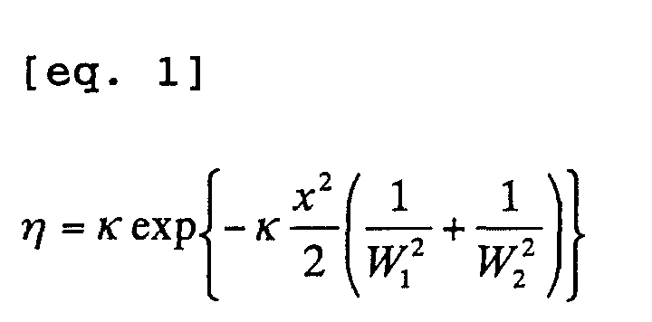
- the coupling efficiency ⁇ may be given by the following equation: where beam spot sizes (the radius that the amplitude of a Gaussian beam becomes 1/e of the median value) in each of beam waists of a semiconductor laser 23 and a waveguide 22 (where the radius of curvature of the wavefront of Gaussian beams is infinite) are W1 and W2 respectively, Z is the distance between these beam waists, X is the offset in the direction perpendicular to the optical axis, ⁇ is the wavelength of beam to be carried.
- K may be given by:
- the beam spot size W1 of a conventional semiconductor laser 23 in other words the incident beam spot size W1 is much smaller when compared with the beam spot size W2 of the optical fiber or waveguide 22 so that W1 will not be equal to W2. It can be concluded that the coupling efficiency will be good.
- the semiconductor laser integrated with the attachment of a beam spot size converter has an effect to approaching W1 to W2 by enlarging W1 in order to improve the coupling efficiency and tolerance as a result.
- a semiconductor laser integrated with the attachment of a beam spot size converter is constructed by using selective crystalline growth technology in order to tapering the film thickness at the emitting end of a core.
- the integration of beam spot size converter may affect the optimum design of the laser used, or the sensitivity of laser characteristics with respect to the construction error.
- the conventional laser system has an insufficient yield, which pushed up the price of laser elements and finally a considerable reduction of cost of the optical modules is not yet achieved.
- the enlargement of beam spot size by tapering by the selective crystalline growth method is limited to, at present, approximately 10 degrees when expressed by the angle of divergence of far field image when approximating a Gaussian beam.
- the divergence of optical fibers is in the order of approximately 5 degrees, the difference between these two is still large.
- an innovative technology of a novel coupling scheme in combination therewith is needed in order to achieve a higher optical coupling efficiency along with ease of construction.
- One solution is to incorporate an optical lens between a semiconductor laser and a waveguide.
- this solution may result in an increase of the number of parts and a complex method of production so that the achievement of lowering cost of optical modules will be difficult.
- a primary object of the present invention is to provide an optical transmission module and an optical communication system allowing the coupling efficiency between optical components to be improved.
- a secondary object of the present invention is to provide an optical transmission module and an optical communication system which may improve at least one of either the coupling efficiency or the tolerance between optical components.
- the present invention comprises: a first optical waveguide for enlarging the spot size of light beam in the direction of propagation of the beam; and a second optical waveguide for shrinking the beam spot size of light beam enlarged by the first waveguide in the direction of beam propagation.
- the present invention may also comprise: at least either of the first optical waveguide or the second optical waveguide including a plurality of cores formed in positions so as to propagate an optical beam in the direction of beam propagation.
- the present invention may also comprise: when defining an optical axis in the propagation direction of the optical beam as z-axis, an optical axis in the vertical direction at an orthogonal section as x-axis, and an optical axis in the horizontal direction as y-axis, at least either of the first optical waveguide or the second optical waveguide including a plurality of cores formed so as to propagate an optical beam in the direction of Z axis; and the width in X axis or Y axis of at least part of the cores varying in the direction of Z axis.
- the present invention comprises: a first optical waveguide for enlarging the spot size of an optical beam in the direction of propagation of the beam; a second optical waveguide for maintaining the beam spot size of optical beam enlarged by the first optical waveguide; and a third optical waveguide for shrinking the beam spot size of optical beam maintained by the second waveguide.
- the expression "maintaining the beam spot size” means that a relation may be established in which the absolute value of the rate of change of the radius of beam spot with respect to the direction of propagation of optical beam in the second optical waveguide is less than the absolute value of the rate of change of the beam spot size with respect to the direction of propagation of optical beam in either one of first or third optical waveguide. More specifically, the relation may be such that the absolute value of the rate of mean refractive index becomes less than 0.05 % when a beam propagates 100 micrometers. Therefore if the value is larger, the beam spot is thought to be enlarged or shrunk.
- the present invention may also comprise: at least either one of the first optical waveguide or the second optical waveguide or the third optical waveguide including a plurality of cores formed in positions so as to propagate an optical beam in the direction of beam propagation.
- the present invention may further comprise: when defining an optical axis in the propagation direction of the optical beam as z-axis, an optical axis in the vertical direction at an orthogonal section as x-axis, and an optical axis in the horizontal direction as y-axis, at least either one of the first optical waveguide or the second optical waveguide or the third optical waveguide including a plurality of cores formed in position so as to propagate an optical beam in the direction of Z axis; and the width in X axis or Y axis of at least part of the cores varying in the direction of Z axis.
- a cladding having a lower index of refraction than the cores is layered, formed between cores in the direction of optical beam propagation.
- reference numeral 23 designates to an light emitting element such as a semiconductor laser, reference numeral 21 to a beam spot size converter waveguide for enlarging then shrinking the beam spot size, or for enlarging and maintaining then shrinking the beam spot size, reference numeral 22 to a waveguide that propagates the optical beam having the beam spot size converted by the beam spot size converter waveguide 21.
- the beam spot size converter waveguide 21 in Fig. 8 (a) includes a beam spot size enlarger waveguide 11 for enlarging the beam spot size to propagate the beam, and a beam spot size reducer waveguide 13 for shrinking the beam spot size to propagate the beam.
- the beam emitted from the light emitting element 23 such as a semiconductor laser will have the beam spot size enlarged by the beam spot size enlarger waveguide 11. Then the spot size-enlarged beam will have the beam spot size shrunk by the beam spot size reducer waveguide 13 to emit into the light waveguide that follows.
- the beam having the beam spot size enlarged by the beam spot size enlarger waveguide 11 will have the beam spot size maintained at the same spot size in the beam spot size maintainer waveguide 12.
- the beam spot radius reducer waveguide 13 then will shrink the beam spot size to propagate into the waveguide that follows.
- the beam propagated by the waveguide 22 will have a beam spot size W2 at one end of the beam spot size converter waveguide 21 (the beam spot size reducer waveguide 13)
- the beam when propagating in the beam spot size reducer waveguide 13, the beam will have the beam spot size enlarged to W3 at the interface of the beam spot size reducer waveguide 13 with the beam spot size enlarger waveguide 11.
- the beam spot size W2 of the beam propagated from the waveguide 22 may be changed to the beam spot size W4 of an arbitrary magnitude.
- the beam spot size converter waveguide 21 allows the beam spot size W2 to be converted to a beam spot size W4 that has a spot size approximately equal to the beam spot size W1, such that the beam spot size W1 may become at or around the beam spot size W4, resulting in an improvement of the coupling efficiency. This can be understood from the above-mentioned equations (1) and (2).
- the beam spot size converter waveguide 21 may also artificially displace the position of the formed beam waist W4 into a proximal position of the light emitting element 23, in other words it may shorten the distance of the beam waists from Z to Z', resulting in an improvement of the coupling efficiency.
- the beam spot size converter waveguide 21 in particular, it will be possible to artificially and apparently bring the beam waist W4 much closer to the light emitting element 23, beyond the physically possible limit of implementing the light emitting element 23 and the waveguide 22.
- the beam propagating the beam spot size waveguide 13 will have the beam spot size enlarged to W3 at the interface of the beam spot size reducer waveguide 13 and beam spot size maintainer waveguide 12, then the beam will pass through the beam spot size maintainer waveguide 12 with the beam spot size maintained, to enter into the beam spot size enlarger waveguide 11.
- the beam spot size at the entrance of beam spot size enlarger waveguide 11 will be W3.
- the architecture shown in Fig. 8 (b) enables the conversion of the beam spot size W2 of the beam having propagated from the waveguide 22 to a give size of beam spot size W4, by incorporating the beam spot size converter waveguide 21, in a manner similar to that shown in Fig. 8 (a).
- the beam spot size converter waveguide 21 allows the beam spot size W2 to be converted to a beam spot size W4 that has a r size approximately equal to the beam spot size W1, such that the beam spot size W1 may become at or around the beam spot size W4, resulting in an improvement of the coupling efficiency.
- the coupling efficiency between a semiconductor laser 23 and the waveguide 22 can be determined by the beam spot sizes (W1 and W4) of respective beam waists as well as the distance Z' between two beam waists. This concludes that an improvement of coupling efficiency may be achieved by using the beam spot size converter waveguide 21 as have been described above to rearrange the beam spot size W2 to the beam spot size W4 that has approximately the same size as the beam spot size W1.
- the beam spot size converter waveguide 21 as have been described above can be formed integral with the waveguide 22, there will not be a substantial discrepancy with the waveguide 22, without any problems associated with an increase of the number of parts or of the complex production.
- Fig. 9 (a) when there is not a beam spot size maintainer waveguide 12, if the incident light beam 3 emitted from a semiconductor laser is running out by a parallel offset (without inclination), the beam having propagated through the beam spot size converter waveguide will have an inclination with respect to the optical axis of incident beam.
- the inclination leads to a disjunction from the proper axis along with the propagation of beam, resulting in a decrease of the intensity of light beam to be propagated to the waveguide 22. This indicates the degradation of tolerance with respect to the axial offset.
- the beam spot size maintainer waveguide 12 when there is a beam spot size maintainer waveguide 12, the light beam 3 having an inclination caused by the beam spot size enlarger waveguide 11 will be collimated by the beam spot size maintainer waveguide 12 so as to run into the proper, intrinsic direction of optical axis. After the compensation for the propagation direction, the beam will have the beam spot size shrunk by the beam spot size reducer waveguide 13 to the size of the waveguide 22 to propagate into the ahead waveguide 22. In other words, by incorporating the beam spot size maintainer waveguide 12, the propagation direction of an inclined beam can be compensated for and corrected to the proper, original propagation direction of the optical axis.
- FIG. 1 A typical example of the structure of the beam spot size converter waveguide 21 is shown in Fig. 1.
- the beam spot size converter waveguide 21 and the waveguide 22 are shown in Fig. 1.
- reference numeral 1 denotes to a core that propagates beams
- the reference numeral 3 is a beam propagating in the waveguide.
- the beam spot radius converter waveguide 21 is built incorporating the beam spot size enlarger waveguide 11, beam spot size maintainer waveguide 12, and beam spot size reducer waveguide 13.
- the difference in the refractive index of the core/cladding is altered in the direction of the propagation of light beam so as to enlarge or shrink the beam spot size.
- the difference in the refractive index of the core/cladding indicates the difference between the mean index of refraction in a segment that combines the cores and claddings, and the index of refraction of the claddings surrounding the segment, in case in which the cores and claddings are alternately compiled in the direction of the propagation of light beam. If the cross-sectional area of the cores in the propagation direction of the light beam is equivalent, the smaller the difference of the core/cladding refractive index, the weaker the light enclosure is so that the beam spot size will be enlarged.
- the principle of segmented waveguide as a means of refractive index conversion that is adopted in the present embodiment will be described herein below.
- Fig. 7 shows a schematic diagram of a segmented waveguide in accordance with the present invention.
- a segmented waveguide in the direction of the propagation of light beam includes a chain composed of a section with a core 1 that has a length and another section without a core 1 that immediately follows (i.e., a segment with a cladding 2).
- n1 is the index of refraction of the clad 2
- n2 is the refractive index of the core 1
- ⁇ is the ratio of the core length to a unit length L
- the n' derived from the equation (1) can be thought of the mean index of refraction in a unit length L.
- n' (1 - ⁇ ) ⁇ n1 + ⁇ ⁇ n2
- the refractive index of the waveguide can be changed. This is the principle of the segmented waveguide as a means of conversion of the index of refraction.
- the principle of the segmented waveguide may be applied to the optical module shown in Fig. 1, in which the ratio ⁇ of the core length of a segment in the beam spot size enlarger waveguide 11 and the beam spot size reducer waveguide 13 is tailored so as to linearly increase or decrease along with the direction of the propagation of light beam, in order to convert the beam spot size.
- the beam spot size enlarger waveguide 11 may be built such that the ratio of the core occupied in a segment in the direction of the propagation of light beam is decreasing while the segment length is invariable.
- the beam spot size reducer waveguide 13 may also be built such that the ratio of the core occupied in a segment in the direction of the propagation of light beam is increasing while the segment length is invariable.
- the beam spot size enlarger waveguide 11 can be such that the core length per se becomes shorter in the direction of the propagation of light beam, in each segment, provided that the gap between cores is nearly constant. In contrary, if the core length is kept nearly constant, the beam spot size enlarger waveguide 11 can be built such that the core length per se becomes larger in the direction of the propagation of light beam in each segment.
- the specific dimension of segments and core 1 in particular can be determined based on the beam spot size of the semiconductor laser used, which is not shown in the figure. It is preferable to design such that the propagation loss of the beam spot size converter waveguide 21 is not excessively larger. For example, a preferable dimension may be such that the segment frequency is 20 micrometers, the length of a core therein is in the range between 10 and 19 micrometers.
- the beam spot size conversion is implemented by using a plurality of segments to achieve a gradual change, in order to avoid the conversion of light beam mode caused by an abrupt modification of beam spot size.
- the mean index of refraction shifts by a nearly constant rate in the range of approximately 0.05 to 0.2 % in the direction of the propagation of light beam when the light beam propagates a distance of 100 micrometers.
- the width in the direction of y-axis of the segment is also altered. This is for the sake of reduction of the diffusion loss during the propagation by emitting beam into a next core.
- the width in the direction of y-axis of the segment needs to be altered in a range that the mode of propagation of the light beam is not modified.
- the width Wy in the direction of y-axis may be given by satisfying an inequality [eq.
- n' is the mean index of refraction of a segment
- n2 is the index of refraction of the cladding
- ⁇ n' (n' - n2)
- the beam spot size maintainer waveguide 12 may be built so as to maintain a nearly constant beam spot size with an invariable ⁇ .
- the end of the beam spot size maintainer waveguide 12 have preferably a beam spot size identical to the end of the beam spot size enlarger waveguide 11 and the beam spot size reducer waveguide 13 so as not to induce coupling loss, however it needs necessarily not to be fixed to a dimension under the condition that the propagation loss stays small.
- the cross-section of the waveguide 22 connected to the beam spot size converter waveguide 21 is 6.5 micrometers square.
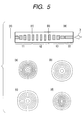
- Fig. 5 depicts an aspect in which the beam spot shape of the light beam 3 incident from the waveguide 22 is converted by the beam spot size converter waveguides 11, 12 and 13.
- (a) is the shape at the entrance of a beam spot size converter waveguide, namely the shape of the beam spot propagating in the waveguide 22.
- (b) is the shape on the connection of the beam spot size reducer waveguide 13 with the beam spot size maintainer waveguide 12, where it can be seen that the beam spot size is enlarged.
- (c) is the shape of the beam spot on the connection of the beam spot size maintainer waveguide 12 with the beam spot size enlarger waveguide 11, where the shape of (b) is almost maintained.
- (d) is the shape of beam spot ahead of the beam spot size enlarger waveguide 11.
- (d) is the beam spot size smaller than (a), indicating that the beam spot size is converted by the beam spot size converter waveguide 21.
- a Si substrate 31 is provided (step (a)).
- first cladding layer 32 and a core layer 33 are deposited on the Si substrate 31, as glass particles obtained by heating hydrolysis of materials in oxygen-hydrogen flame (step (b)).
- the core layer 33 has a higher concentration of dopant such as titanium oxide and germanium oxide.
- This process is referred to as a flame hydrolysis deposition, well known in the art as a production method of quartz waveguides. Thereafter the film of glass particles will be heated in an electric furnace to a high temperature to transparentize (step (b)).
- the core patterns for the beam spot size converter waveguide 21 and the waveguide 22 connected thereto will be formed simultaneously on the core layer 33, by means of usual photolithography. For example, after applying some resist and transferring a mask pattern, the layer will be etched to a predetermined depth by RIE (reactive ion etching) to form the core patterns (step (c)).
- RIE reactive ion etching
- Second cladding layer 34 with the amount of dopant adjusted so as to yield a lower index of refraction than the core layer 33 will be deposited thereon as glass particles, and then the substrate will be heated to a high temperature to transparentize (step (d)).
- a quartz material When a quartz material is used, a trace amount of dopant(s) is often added to assist to adjust the temperature of glass softening and the coefficient of thermal expansion.
- other materials including but not limited to polymers may also be used instead of quartz glass provided that the light in the wavelength band used can be transmitted and that the index of refraction can be fine tuned.
- the above steps will form integrally the beam spot size converter waveguide 21 with the waveguide 22 connected thereto. Since the beam spot size converter waveguide 21 can be formed integrated with the waveguide 22, there will be no substantial offset with the waveguide, without any problems associated with an increase of the number of parts or of the complex production. It is needless to say that the above-cited manufacturing steps may also be applied to the structure of following embodiments as well.
- the beam spot size converter waveguide 21 is different from the first preferred embodiment as have been described above, in that it is composed of the beam spot size enlarger waveguide 11 and the beam spot size reducer waveguide 13.
- the second embodiment also uses the segmented structure to linearly increase or decrease the ratio ⁇ of the core length in a segment in the direction of the propagation of light beam, as well as the width of a segment in the direction of y-axis, in order to convert the beam spot size.
- the beam spot size maintainer waveguide 12 is omitted to save spaces to make the waveguide smaller than the first preferred embodiment described above, while having an effect that suppresses the light beam loss during propagation. It is also needless to say that the coupling efficiency will be increased when compared to the prior art.
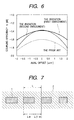
- Fig. 6 shows a graph illustrating the coupling efficiency and the tolerance between a semiconductor laser and a waveguide, implemented by using the beam spot size converter waveguide 11 of the second preferred embodiment of the present invention.
- the graph of Fig. 6 there is also shown a result for the sake of comparison when the beam spot size converter waveguide is not used.
- the graph is based on the results obtained by the simulation in the beam propagation method (BPM), as similar to Fig. 5.
- another method of beam spot size conversion with respect to the beam spot size enlarger waveguide 11 is applied to modify the cross-sectional area of core along with the direction of the propagation of light beam.
- This method is applied to the beam spot radius converter waveguide 21 shown in Fig. 2, however this is equally applied to the waveguide shown in Fig. 1.
- the cross-sectional area of the core is varied along with the direction of the propagation of light beam, i.e., tapered.
- the tapered shape is formed only in y-axis, namely in the direction of an axis in parallel to the substrate surface, while the shape is constant in the x-axis.
- the beam spot size can be enlarged or shrunk in both x- and y-axis.
- the beam spot size When decreasing the cross-sectional area of core along with the direction of the propagation of light beam the beam spot size will be reduced to a certain level, and will be enlarged when further decreasing because of the light enclosed in the core will be weakened. Therefore, the beam spot size can be enlarged to a certain desirable size by adjusting the taper in the beam spot size enlarger waveguide 11.
- a beam spot size converter waveguide of the shape thus formed may also alter the coupling efficiency.
- the coupling efficiency may be improved as similar to the foregoing embodiments, with the tolerance of the axial offset maintained.
- the present invention may be embodied in other specific forms without departing from the spirit or essential characteristics thereof.
- another method of converting difference in the index of refraction other than those cited above can be devised by using materials having different index of refraction.
- an optical module and optical communication system may be provided, which improves the coupling efficiency between optical parts. Also in accordance with the present invention, an optical module and optical communication system may be provided in which either of the coupling efficiency between optical parts or the tolerance may be improved.
Landscapes
- Physics & Mathematics (AREA)
- Engineering & Computer Science (AREA)
- General Physics & Mathematics (AREA)
- Optics & Photonics (AREA)
- Microelectronics & Electronic Packaging (AREA)
- Power Engineering (AREA)
- Optical Couplings Of Light Guides (AREA)
- Optical Integrated Circuits (AREA)
- Optical Communication System (AREA)
Abstract
Description

Claims (8)
- An optical module, comprising:a first optical waveguide for enlarging the spot size of light beam in the direction of propagation of the beam; anda second optical waveguide for shrinking the spot size of light beam enlarged by said first waveguide in the direction of beam propagation.
- An optical module according to claim 1, further comprising:
at least either of said first optical waveguide or said second optical waveguide including a plurality of cores formed in positions so as to propagate the light beam in the direction of beam propagation. - An optical module according to claim 1, further comprising:when defining an optical axis in the propagation direction of the optical beam as z-axis, an optical axis in the vertical direction at an orthogonal section as x-axis, and an optical axis in the horizontal direction as y-axis,at least either of said first optical waveguide or said second optical waveguide including a plurality of cores formed so as to propagate the light beam in the direction of z-axis; andthe width in x-axis or y-axis of at least part of the cores varying in the direction of z-axis.
- An optical module, comprising:a first optical waveguide for enlarging the spot size of an optical beam in the direction of propagation of the beam;a second optical waveguide for maintaining the spot size of optical beam enlarged by said first optical waveguide; anda third optical waveguide for shrinking the spot size of optical beam maintained by said second optical waveguide.
- An optical module according to claim 4, further comprising:
at least either one of said first optical waveguide or said second optical waveguide or said third optical waveguide including a plurality of cores formed in positions so as to propagate the light beam in the direction of light beam propagation. - An optical module according to claim 5, further comprising:when defining an optical axis in the propagation direction of the light beam as z-axis, an optical axis in the vertical direction at an orthogonal section as x-axis, and an optical axis in the horizontal direction as y-axis,at least either one of said first optical waveguide or said second optical waveguide or said third optical waveguide including a plurality of cores formed in position so as to propagate an optical beam in the direction of z-axis; andthe width in x-axis or y-axis of at least part of said cores varying in the direction of z axis.
- An optical module according to one of claims 2, 3, 5 and 6, further comprising:
a cladding which has a lower refractive index than the cores being layered, formed between the cores in the direction of the propagation of light beam. - An optical communication system, comprising:
optical modules according to any one of claims 1 to 7.
Applications Claiming Priority (2)
| Application Number | Priority Date | Filing Date | Title |
|---|---|---|---|
| JP2000126230A JP3941334B2 (en) | 2000-04-20 | 2000-04-20 | Optical transmission module and optical communication system using the same |
| JP2000126230 | 2000-04-20 |
Publications (3)
| Publication Number | Publication Date |
|---|---|
| EP1148357A2 true EP1148357A2 (en) | 2001-10-24 |
| EP1148357A3 EP1148357A3 (en) | 2003-06-25 |
| EP1148357B1 EP1148357B1 (en) | 2006-02-01 |
Family
ID=18636049
Family Applications (1)
| Application Number | Title | Priority Date | Filing Date |
|---|---|---|---|
| EP01301837A Expired - Lifetime EP1148357B1 (en) | 2000-04-20 | 2001-02-28 | Optical transmission module and optical communication system using the same |
Country Status (4)
| Country | Link |
|---|---|
| US (1) | US6937799B2 (en) |
| EP (1) | EP1148357B1 (en) |
| JP (1) | JP3941334B2 (en) |
| DE (1) | DE60116958T2 (en) |
Cited By (2)
| Publication number | Priority date | Publication date | Assignee | Title |
|---|---|---|---|---|
| WO2018130285A1 (en) * | 2017-01-12 | 2018-07-19 | Telefonaktiebolaget Lm Ericsson (Publ) | Apparatus and method for coupling light |
| US11506850B2 (en) * | 2018-12-13 | 2022-11-22 | Sony Group Corporation | Optical connector, optical cable, and electronic device |
Families Citing this family (17)
| Publication number | Priority date | Publication date | Assignee | Title |
|---|---|---|---|---|
| KR100475410B1 (en) * | 2002-03-13 | 2005-03-10 | 주식회사 럭스퍼트 | Arrayed optical device having enhanced pump efficiency |
| US7480214B2 (en) * | 2003-12-08 | 2009-01-20 | Seagate Technology Llc | Efficient waveguide coupler for data recording transducer |
| US6931180B2 (en) * | 2004-01-13 | 2005-08-16 | Lucent Technologies Inc. | Method and apparatus for compactly coupling an optical fiber and a planar optical waveguide |
| JP2006126658A (en) * | 2004-10-29 | 2006-05-18 | Nippon Telegr & Teleph Corp <Ntt> | Optical waveguide device |
| US7356226B2 (en) * | 2005-03-30 | 2008-04-08 | Nec Corporation | Optical waveguide coupler, sub-assembled optical unit, optical module and optically coupling method |
| JP2006350115A (en) * | 2005-06-17 | 2006-12-28 | Nippon Telegr & Teleph Corp <Ntt> | Optical circuit and optical circuit manufacturing method |
| KR100754597B1 (en) * | 2006-01-03 | 2007-09-05 | 삼성전자주식회사 | Optical mode size converter integrated laser device and manufacturing method thereof |
| US7680371B2 (en) * | 2007-02-13 | 2010-03-16 | National Research Council Of Canada | Interface device for performing mode transformation in optical waveguides |
| US20090310912A1 (en) * | 2008-06-17 | 2009-12-17 | Serge Bidnyk | Integrated wavelength locker and multiplexer |
| US8571362B1 (en) * | 2009-03-30 | 2013-10-29 | Mellanox Technologies Ltd. | Forming optical device using multiple mask formation techniques |
| TW201421077A (en) * | 2012-11-30 | 2014-06-01 | Hon Hai Prec Ind Co Ltd | Lens module and optical fiber coupled connecter |
| JP5837015B2 (en) * | 2013-09-30 | 2015-12-24 | 沖電気工業株式会社 | Semiconductor laser module and manufacturing method thereof |
| EP2887110A1 (en) * | 2013-12-20 | 2015-06-24 | IMEC vzw | Integrated photonic coupler |
| KR20190115757A (en) * | 2018-04-03 | 2019-10-14 | 한국전자통신연구원 | Optical circuit element |
| ES2872650B2 (en) * | 2020-04-29 | 2022-03-11 | Univ Malaga | BRICKED SUB-WAVELENGTH PERIODIC WAVEGUIDE, MODAL ADAPTER, POWER SPLITTER AND POLARIZATION SPLITTER MAKE USE OF SUCH WAVEGUIDE |
| JP7510079B2 (en) * | 2020-08-03 | 2024-07-03 | 日本電信電話株式会社 | Optical Circuit |
| US11409040B1 (en) * | 2021-03-23 | 2022-08-09 | Globalfoundries U.S. Inc. | Optical couplers for ridge-to-rib waveguide core transitions |
Family Cites Families (16)
| Publication number | Priority date | Publication date | Assignee | Title |
|---|---|---|---|---|
| JPS5041559A (en) * | 1973-08-02 | 1975-04-16 | ||
| JPH03288102A (en) * | 1990-04-04 | 1991-12-18 | Fujitsu Ltd | Manufacture of light beam shape converting element |
| JPH05249331A (en) | 1992-01-09 | 1993-09-28 | Nippon Telegr & Teleph Corp <Ntt> | Waveguide type beam spot conversion element and production thereof |
| JP3049697B2 (en) * | 1992-07-29 | 2000-06-05 | 住友電気工業株式会社 | Mode field diameter conversion fiber |
| FR2715232B1 (en) * | 1994-01-19 | 1996-02-16 | Commissariat Energie Atomique | Method for optimizing a path of an optical guide and optical guide obtained by this method. |
| US5577141A (en) * | 1995-03-10 | 1996-11-19 | Lucent Technologies Inc. | Two-dimensional segmentation mode tapering for integrated optic waveguides |
| JPH0949947A (en) * | 1995-08-10 | 1997-02-18 | Hitachi Ltd | Optical module |
| US5761364A (en) * | 1995-11-02 | 1998-06-02 | Motorola, Inc. | Optical waveguide |
| JP3006832B2 (en) * | 1996-05-14 | 2000-02-07 | 日本電気株式会社 | Optical coupling structure between light emitting device and optical waveguide |
| KR100189855B1 (en) * | 1996-11-18 | 1999-06-01 | 윤종용 | Optical couplers with mode-evaluation and their fabrication method |
| US6112002A (en) * | 1996-11-29 | 2000-08-29 | Fujitsu Limited | Optical coupler optically coupling a light beam of a semiconductor laser source with a single mode optical waveguide or fiber |
| US5862288A (en) * | 1997-04-21 | 1999-01-19 | The United States Of America As Represented By The Secretary Of The Army | Self-imaging waveguide devices for wavelength division multiplexing applications |
| JP3104789B2 (en) * | 1997-05-02 | 2000-10-30 | 日本電気株式会社 | Semiconductor optical device and method of manufacturing the same |
| JP3663310B2 (en) | 1999-01-26 | 2005-06-22 | 株式会社日立製作所 | Optical beam spot converter, optical transmission module and optical transmission system using the same |
| US6243517B1 (en) * | 1999-11-04 | 2001-06-05 | Sparkolor Corporation | Channel-switched cross-connect |
| US6293688B1 (en) * | 1999-11-12 | 2001-09-25 | Sparkolor Corporation | Tapered optical waveguide coupler |
-
2000
- 2000-04-20 JP JP2000126230A patent/JP3941334B2/en not_active Expired - Lifetime
-
2001
- 2001-02-28 DE DE60116958T patent/DE60116958T2/en not_active Expired - Lifetime
- 2001-02-28 US US09/793,923 patent/US6937799B2/en not_active Expired - Fee Related
- 2001-02-28 EP EP01301837A patent/EP1148357B1/en not_active Expired - Lifetime
Cited By (3)
| Publication number | Priority date | Publication date | Assignee | Title |
|---|---|---|---|---|
| WO2018130285A1 (en) * | 2017-01-12 | 2018-07-19 | Telefonaktiebolaget Lm Ericsson (Publ) | Apparatus and method for coupling light |
| US10852484B2 (en) | 2017-01-12 | 2020-12-01 | Telefonaktiebolaget Lm Ericcson (Publ) | Apparatus and method for coupling light |
| US11506850B2 (en) * | 2018-12-13 | 2022-11-22 | Sony Group Corporation | Optical connector, optical cable, and electronic device |
Also Published As
| Publication number | Publication date |
|---|---|
| DE60116958D1 (en) | 2006-04-13 |
| JP2001305366A (en) | 2001-10-31 |
| EP1148357A3 (en) | 2003-06-25 |
| JP3941334B2 (en) | 2007-07-04 |
| US20010036338A1 (en) | 2001-11-01 |
| EP1148357B1 (en) | 2006-02-01 |
| DE60116958T2 (en) | 2006-07-27 |
| US6937799B2 (en) | 2005-08-30 |
Similar Documents
| Publication | Publication Date | Title |
|---|---|---|
| EP1148357A2 (en) | Optical transmission module and optical communication system using the same | |
| JP3581224B2 (en) | Planar optical waveguide device | |
| US7058259B2 (en) | Optical device having a waveguide lens with multimode interference | |
| US7554741B2 (en) | Optical transmission device and light-receiving module | |
| JP3563376B2 (en) | Manufacturing method of optical multiplexer / demultiplexer | |
| JP3941368B2 (en) | Optical transmission module and optical communication system using the same | |
| US6553164B1 (en) | Y-branch waveguide | |
| JP3841969B2 (en) | Y branch optical waveguide and optical integrated circuit | |
| JP2023040871A (en) | Optical waveguide device and optical integrated circuit | |
| US7046881B2 (en) | Manufacturing method for optical coupler/splitter and method for adjusting optical characteristics of planar lightwave circuit device | |
| US6587629B1 (en) | Optical waveguide channel device | |
| US11048045B1 (en) | Integrated lens mode size converter | |
| EP2224269B1 (en) | Manufacturing method of an optical waveguide dispersion compensating device | |
| JP3258542B2 (en) | Branch-joining optical waveguide | |
| JP5091072B2 (en) | Y branch optical waveguide and design method thereof | |
| JP2002090561A (en) | Optical multiplexer / demultiplexer | |
| JP3093362B2 (en) | Optical directional coupler | |
| JP2003035832A (en) | Polarization-independent directional coupler and optical circuit using the same | |
| JPH08292340A (en) | Optical branch | |
| WO2001090791A1 (en) | Optical module | |
| US5440656A (en) | Waveguide type optical component having optical coupling sections with different coupling efficiencies | |
| JP2000329951A (en) | Waveguide type multi-light source unit | |
| JP2002169046A (en) | Optical transmission module and optical communication system using the same | |
| JP2004240064A (en) | Spot size conversion optical waveguide, optical module and waveguide type optical circuit | |
| CA2184453C (en) | Optical device formed with grating therein, add/drop filter using same, and method of fabricating same |
Legal Events
| Date | Code | Title | Description |
|---|---|---|---|
| PUAI | Public reference made under article 153(3) epc to a published international application that has entered the european phase |
Free format text: ORIGINAL CODE: 0009012 |
|
| 17P | Request for examination filed |
Effective date: 20010319 |
|
| AK | Designated contracting states |
Kind code of ref document: A2 Designated state(s): AT BE CH CY DE DK ES FI FR GB GR IE IT LI LU MC NL PT SE TR |
|
| AX | Request for extension of the european patent |
Free format text: AL;LT;LV;MK;RO;SI |
|
| PUAL | Search report despatched |
Free format text: ORIGINAL CODE: 0009013 |
|
| AK | Designated contracting states |
Designated state(s): AT BE CH CY DE DK ES FI FR GB GR IE IT LI LU MC NL PT SE TR |
|
| AX | Request for extension of the european patent |
Extension state: AL LT LV MK RO SI |
|
| RIC1 | Information provided on ipc code assigned before grant |
Ipc: 7G 02B 6/26 B Ipc: 7G 02B 6/122 A Ipc: 7G 02B 6/12 B |
|
| 17Q | First examination report despatched |
Effective date: 20040112 |
|
| AKX | Designation fees paid |
Designated state(s): DE FR GB |
|
| GRAP | Despatch of communication of intention to grant a patent |
Free format text: ORIGINAL CODE: EPIDOSNIGR1 |
|
| RIC1 | Information provided on ipc code assigned before grant |
Ipc: 7G 02B 6/26 B Ipc: 7G 02B 6/122 B Ipc: 7G 02B 6/14 A |
|
| RAP1 | Party data changed (applicant data changed or rights of an application transferred) |
Owner name: OPNEXT JAPAN, INC. |
|
| GRAS | Grant fee paid |
Free format text: ORIGINAL CODE: EPIDOSNIGR3 |
|
| GRAA | (expected) grant |
Free format text: ORIGINAL CODE: 0009210 |
|
| AK | Designated contracting states |
Kind code of ref document: B1 Designated state(s): DE FR GB |
|
| REG | Reference to a national code |
Ref country code: GB Ref legal event code: FG4D |
|
| REF | Corresponds to: |
Ref document number: 60116958 Country of ref document: DE Date of ref document: 20060413 Kind code of ref document: P |
|
| ET | Fr: translation filed | ||
| PLBE | No opposition filed within time limit |
Free format text: ORIGINAL CODE: 0009261 |
|
| STAA | Information on the status of an ep patent application or granted ep patent |
Free format text: STATUS: NO OPPOSITION FILED WITHIN TIME LIMIT |
|
| 26N | No opposition filed |
Effective date: 20061103 |
|
| PGFP | Annual fee paid to national office [announced via postgrant information from national office to epo] |
Ref country code: FR Payment date: 20140211 Year of fee payment: 14 |
|
| PGFP | Annual fee paid to national office [announced via postgrant information from national office to epo] |
Ref country code: GB Payment date: 20140226 Year of fee payment: 14 |
|
| PGFP | Annual fee paid to national office [announced via postgrant information from national office to epo] |
Ref country code: DE Payment date: 20140417 Year of fee payment: 14 |
|
| REG | Reference to a national code |
Ref country code: DE Ref legal event code: R119 Ref document number: 60116958 Country of ref document: DE |
|
| GBPC | Gb: european patent ceased through non-payment of renewal fee |
Effective date: 20150228 |
|
| REG | Reference to a national code |
Ref country code: FR Ref legal event code: ST Effective date: 20151030 |
|
| PG25 | Lapsed in a contracting state [announced via postgrant information from national office to epo] |
Ref country code: DE Free format text: LAPSE BECAUSE OF NON-PAYMENT OF DUE FEES Effective date: 20150901 Ref country code: GB Free format text: LAPSE BECAUSE OF NON-PAYMENT OF DUE FEES Effective date: 20150228 |
|
| PG25 | Lapsed in a contracting state [announced via postgrant information from national office to epo] |
Ref country code: FR Free format text: LAPSE BECAUSE OF NON-PAYMENT OF DUE FEES Effective date: 20150302 |