EP1146552A2 - Interconnections to copper ICs - Google Patents
Interconnections to copper ICs Download PDFInfo
- Publication number
- EP1146552A2 EP1146552A2 EP01303322A EP01303322A EP1146552A2 EP 1146552 A2 EP1146552 A2 EP 1146552A2 EP 01303322 A EP01303322 A EP 01303322A EP 01303322 A EP01303322 A EP 01303322A EP 1146552 A2 EP1146552 A2 EP 1146552A2
- Authority
- EP
- European Patent Office
- Prior art keywords
- layer
- copper
- semiconductor integrated
- integrated circuit
- depositing
- Prior art date
- Legal status (The legal status is an assumption and is not a legal conclusion. Google has not performed a legal analysis and makes no representation as to the accuracy of the status listed.)
- Granted
Links
Images


Classifications
-
- H—ELECTRICITY
- H10—SEMICONDUCTOR DEVICES; ELECTRIC SOLID-STATE DEVICES NOT OTHERWISE PROVIDED FOR
- H10W—GENERIC PACKAGES, INTERCONNECTIONS, CONNECTORS OR OTHER CONSTRUCTIONAL DETAILS OF DEVICES COVERED BY CLASS H10
- H10W72/00—Interconnections or connectors in packages
- H10W72/071—Connecting or disconnecting
-
- H—ELECTRICITY
- H10—SEMICONDUCTOR DEVICES; ELECTRIC SOLID-STATE DEVICES NOT OTHERWISE PROVIDED FOR
- H10W—GENERIC PACKAGES, INTERCONNECTIONS, CONNECTORS OR OTHER CONSTRUCTIONAL DETAILS OF DEVICES COVERED BY CLASS H10
- H10W72/00—Interconnections or connectors in packages
- H10W72/01—Manufacture or treatment
- H10W72/012—Manufacture or treatment of bump connectors, dummy bumps or thermal bumps
-
- H—ELECTRICITY
- H10—SEMICONDUCTOR DEVICES; ELECTRIC SOLID-STATE DEVICES NOT OTHERWISE PROVIDED FOR
- H10W—GENERIC PACKAGES, INTERCONNECTIONS, CONNECTORS OR OTHER CONSTRUCTIONAL DETAILS OF DEVICES COVERED BY CLASS H10
- H10W72/00—Interconnections or connectors in packages
- H10W72/071—Connecting or disconnecting
- H10W72/075—Connecting or disconnecting of bond wires
-
- H—ELECTRICITY
- H10—SEMICONDUCTOR DEVICES; ELECTRIC SOLID-STATE DEVICES NOT OTHERWISE PROVIDED FOR
- H10W—GENERIC PACKAGES, INTERCONNECTIONS, CONNECTORS OR OTHER CONSTRUCTIONAL DETAILS OF DEVICES COVERED BY CLASS H10
- H10W72/00—Interconnections or connectors in packages
- H10W72/01—Manufacture or treatment
- H10W72/019—Manufacture or treatment of bond pads
-
- H—ELECTRICITY
- H10—SEMICONDUCTOR DEVICES; ELECTRIC SOLID-STATE DEVICES NOT OTHERWISE PROVIDED FOR
- H10W—GENERIC PACKAGES, INTERCONNECTIONS, CONNECTORS OR OTHER CONSTRUCTIONAL DETAILS OF DEVICES COVERED BY CLASS H10
- H10W72/00—Interconnections or connectors in packages
- H10W72/01—Manufacture or treatment
- H10W72/019—Manufacture or treatment of bond pads
- H10W72/01951—Changing the shapes of bond pads
- H10W72/01955—Changing the shapes of bond pads by using masks
-
- H—ELECTRICITY
- H10—SEMICONDUCTOR DEVICES; ELECTRIC SOLID-STATE DEVICES NOT OTHERWISE PROVIDED FOR
- H10W—GENERIC PACKAGES, INTERCONNECTIONS, CONNECTORS OR OTHER CONSTRUCTIONAL DETAILS OF DEVICES COVERED BY CLASS H10
- H10W72/00—Interconnections or connectors in packages
- H10W72/20—Bump connectors, e.g. solder bumps or copper pillars; Dummy bumps; Thermal bumps
- H10W72/241—Dispositions, e.g. layouts
- H10W72/242—Dispositions, e.g. layouts relative to the surface, e.g. recessed, protruding
-
- H—ELECTRICITY
- H10—SEMICONDUCTOR DEVICES; ELECTRIC SOLID-STATE DEVICES NOT OTHERWISE PROVIDED FOR
- H10W—GENERIC PACKAGES, INTERCONNECTIONS, CONNECTORS OR OTHER CONSTRUCTIONAL DETAILS OF DEVICES COVERED BY CLASS H10
- H10W72/00—Interconnections or connectors in packages
- H10W72/20—Bump connectors, e.g. solder bumps or copper pillars; Dummy bumps; Thermal bumps
- H10W72/251—Materials
-
- H—ELECTRICITY
- H10—SEMICONDUCTOR DEVICES; ELECTRIC SOLID-STATE DEVICES NOT OTHERWISE PROVIDED FOR
- H10W—GENERIC PACKAGES, INTERCONNECTIONS, CONNECTORS OR OTHER CONSTRUCTIONAL DETAILS OF DEVICES COVERED BY CLASS H10
- H10W72/00—Interconnections or connectors in packages
- H10W72/20—Bump connectors, e.g. solder bumps or copper pillars; Dummy bumps; Thermal bumps
- H10W72/251—Materials
- H10W72/252—Materials comprising solid metals or solid metalloids, e.g. PbSn, Ag or Cu
-
- H—ELECTRICITY
- H10—SEMICONDUCTOR DEVICES; ELECTRIC SOLID-STATE DEVICES NOT OTHERWISE PROVIDED FOR
- H10W—GENERIC PACKAGES, INTERCONNECTIONS, CONNECTORS OR OTHER CONSTRUCTIONAL DETAILS OF DEVICES COVERED BY CLASS H10
- H10W72/00—Interconnections or connectors in packages
- H10W72/20—Bump connectors, e.g. solder bumps or copper pillars; Dummy bumps; Thermal bumps
- H10W72/29—Bond pads specially adapted therefor
-
- H—ELECTRICITY
- H10—SEMICONDUCTOR DEVICES; ELECTRIC SOLID-STATE DEVICES NOT OTHERWISE PROVIDED FOR
- H10W—GENERIC PACKAGES, INTERCONNECTIONS, CONNECTORS OR OTHER CONSTRUCTIONAL DETAILS OF DEVICES COVERED BY CLASS H10
- H10W72/00—Interconnections or connectors in packages
- H10W72/50—Bond wires
- H10W72/521—Structures or relative sizes of bond wires
- H10W72/522—Multilayered bond wires, e.g. having a coating concentric around a core
-
- H—ELECTRICITY
- H10—SEMICONDUCTOR DEVICES; ELECTRIC SOLID-STATE DEVICES NOT OTHERWISE PROVIDED FOR
- H10W—GENERIC PACKAGES, INTERCONNECTIONS, CONNECTORS OR OTHER CONSTRUCTIONAL DETAILS OF DEVICES COVERED BY CLASS H10
- H10W72/00—Interconnections or connectors in packages
- H10W72/50—Bond wires
- H10W72/521—Structures or relative sizes of bond wires
- H10W72/522—Multilayered bond wires, e.g. having a coating concentric around a core
- H10W72/523—Multilayered bond wires, e.g. having a coating concentric around a core characterised by the structures of the outermost layers, e.g. multilayered coatings
-
- H—ELECTRICITY
- H10—SEMICONDUCTOR DEVICES; ELECTRIC SOLID-STATE DEVICES NOT OTHERWISE PROVIDED FOR
- H10W—GENERIC PACKAGES, INTERCONNECTIONS, CONNECTORS OR OTHER CONSTRUCTIONAL DETAILS OF DEVICES COVERED BY CLASS H10
- H10W72/00—Interconnections or connectors in packages
- H10W72/50—Bond wires
- H10W72/531—Shapes of wire connectors
- H10W72/536—Shapes of wire connectors the connected ends being ball-shaped
-
- H—ELECTRICITY
- H10—SEMICONDUCTOR DEVICES; ELECTRIC SOLID-STATE DEVICES NOT OTHERWISE PROVIDED FOR
- H10W—GENERIC PACKAGES, INTERCONNECTIONS, CONNECTORS OR OTHER CONSTRUCTIONAL DETAILS OF DEVICES COVERED BY CLASS H10
- H10W72/00—Interconnections or connectors in packages
- H10W72/50—Bond wires
- H10W72/551—Materials of bond wires
- H10W72/552—Materials of bond wires comprising metals or metalloids, e.g. silver
-
- H—ELECTRICITY
- H10—SEMICONDUCTOR DEVICES; ELECTRIC SOLID-STATE DEVICES NOT OTHERWISE PROVIDED FOR
- H10W—GENERIC PACKAGES, INTERCONNECTIONS, CONNECTORS OR OTHER CONSTRUCTIONAL DETAILS OF DEVICES COVERED BY CLASS H10
- H10W72/00—Interconnections or connectors in packages
- H10W72/50—Bond wires
- H10W72/551—Materials of bond wires
- H10W72/552—Materials of bond wires comprising metals or metalloids, e.g. silver
- H10W72/5522—Materials of bond wires comprising metals or metalloids, e.g. silver comprising gold [Au]
-
- H—ELECTRICITY
- H10—SEMICONDUCTOR DEVICES; ELECTRIC SOLID-STATE DEVICES NOT OTHERWISE PROVIDED FOR
- H10W—GENERIC PACKAGES, INTERCONNECTIONS, CONNECTORS OR OTHER CONSTRUCTIONAL DETAILS OF DEVICES COVERED BY CLASS H10
- H10W72/00—Interconnections or connectors in packages
- H10W72/50—Bond wires
- H10W72/551—Materials of bond wires
- H10W72/552—Materials of bond wires comprising metals or metalloids, e.g. silver
- H10W72/5524—Materials of bond wires comprising metals or metalloids, e.g. silver comprising aluminium [Al]
-
- H—ELECTRICITY
- H10—SEMICONDUCTOR DEVICES; ELECTRIC SOLID-STATE DEVICES NOT OTHERWISE PROVIDED FOR
- H10W—GENERIC PACKAGES, INTERCONNECTIONS, CONNECTORS OR OTHER CONSTRUCTIONAL DETAILS OF DEVICES COVERED BY CLASS H10
- H10W72/00—Interconnections or connectors in packages
- H10W72/50—Bond wires
- H10W72/551—Materials of bond wires
- H10W72/555—Materials of bond wires of outermost layers of multilayered bond wires, e.g. material of a coating
-
- H—ELECTRICITY
- H10—SEMICONDUCTOR DEVICES; ELECTRIC SOLID-STATE DEVICES NOT OTHERWISE PROVIDED FOR
- H10W—GENERIC PACKAGES, INTERCONNECTIONS, CONNECTORS OR OTHER CONSTRUCTIONAL DETAILS OF DEVICES COVERED BY CLASS H10
- H10W72/00—Interconnections or connectors in packages
- H10W72/50—Bond wires
- H10W72/59—Bond pads specially adapted therefor
-
- H—ELECTRICITY
- H10—SEMICONDUCTOR DEVICES; ELECTRIC SOLID-STATE DEVICES NOT OTHERWISE PROVIDED FOR
- H10W—GENERIC PACKAGES, INTERCONNECTIONS, CONNECTORS OR OTHER CONSTRUCTIONAL DETAILS OF DEVICES COVERED BY CLASS H10
- H10W72/00—Interconnections or connectors in packages
- H10W72/90—Bond pads, in general
-
- H—ELECTRICITY
- H10—SEMICONDUCTOR DEVICES; ELECTRIC SOLID-STATE DEVICES NOT OTHERWISE PROVIDED FOR
- H10W—GENERIC PACKAGES, INTERCONNECTIONS, CONNECTORS OR OTHER CONSTRUCTIONAL DETAILS OF DEVICES COVERED BY CLASS H10
- H10W72/00—Interconnections or connectors in packages
- H10W72/90—Bond pads, in general
- H10W72/921—Structures or relative sizes of bond pads
- H10W72/923—Bond pads having multiple stacked layers
-
- H—ELECTRICITY
- H10—SEMICONDUCTOR DEVICES; ELECTRIC SOLID-STATE DEVICES NOT OTHERWISE PROVIDED FOR
- H10W—GENERIC PACKAGES, INTERCONNECTIONS, CONNECTORS OR OTHER CONSTRUCTIONAL DETAILS OF DEVICES COVERED BY CLASS H10
- H10W72/00—Interconnections or connectors in packages
- H10W72/90—Bond pads, in general
- H10W72/951—Materials of bond pads
- H10W72/952—Materials of bond pads comprising metals or metalloids, e.g. PbSn, Ag or Cu
Definitions
- This invention relates to integrated circuit packages with copper metallization and wire bond or solder bump bond interconnections.
- Wire bonding has been used in integrated circuit packaging since the inception of IC technology. Wire bonding techniques and wire bonding machines have been refined to the point where wire bonds are relatively inexpensive and are highly reliable. However, wire bonds are rapidly being replaced by more advanced packaging approaches, partly because wire bonds require greater pitch than is available in many state of the art packages.
- interconnection pitches can be very small.
- the earlier technology of wire bonding is being replaced for many applications where the high density of I/O's in current IC chips presents a challenge to the capacity of wire bond techniques.
- packaging yield using advanced packaging techniques may suffer, and the complexity of the packaging process is increased.
- the overall cost per bond may be relatively high.
- the low cost and high reliability of wire bonds makes them attractive if ways can be found to adapt wire bonding to packaging high density I/O chips.
- Interconnection technology faces a new challenge with the introduction of copper metallization in semiconductor IC devices. Copper has long been an attractive candidate as an interconnection material because of its low cost and high conductivity. However, copper is electrochemically active, and migrates in an electrical environment. It also forms undesirable alloys with common materials used in ICs. These assumed drawbacks have limited the introduction of copper metallization in IC manufacture. However, the conductivity advantage that copper presents is so compelling in state of the art high frequency devices that copper has new impetus as a replacement for aluminum in IC chip interconnections.
- solder bump bonding required special under bump metallization (UBM) for the aluminum pads due to the difficulty in soldering directly to aluminum.
- UBM under bump metallization
- solder bump bonds can be made directly to the top copper metallization level.
- solder bump bonding directly to copper IC chip metallization does not overcome the copper migration problem.
- effective UBM technologies for solder bumps on copper metallization are sought.
- the primary function of this UBM in contrast to the UBM used on aluminum metallization, is to form a barrier against copper migration.
- a silicon substrate 11 is shown partially cut away to indicate that is a portion of a much larger silicon wafer. It will be understood that these drawings are not to scale, and some features are shown exaggerated for convenience in this exposition.
- deposited dielectric is shown at 12 and copper contact pad at 13.
- the objective is to cover the copper contact pad 13 with a structure that functions in one case as an under bump metallization (UBM) and in the other case a bond pad for a gold wire bond.
- UBM under bump metallization
- the layered structure that serves for both applications which is referred to here as the common composite, is described in connection with Figs. 2-6.
- the common composite is formed by evaporating or sputtering multiple layers in the sequence described. Sputtering is generally preferred for this step.
- the layers are sputtered in a sputtering apparatus containing multiple targets of the metals of the layers being formed.
- Sputtering techniques are well known and the details are not necessary for this description.
- Other techniques for depositing the metal layers e.g. evaporation or chemical vapor deposition, can also be used.
- the first layer 21 is either chromium or titanium with a thickness of the order of 100-1500 Angstroms. Both chromium and titanium adhere well to the copper contact 13 and also adhere to the dielectric layers present in the structure. These materials are also refractory and form a corrosion resistant interface with the copper contact. It is recommended that titanium layers be sputtered at 300-450 °C , with a layer thickness in the range 200-500 Angstroms.
- the relatively high sputtering temperature encourages the formation of a transition layer of Cu-Ti, which improves adhesion and also improves anti-electromigration lifetime. For some applications, notably those that require high temperature processing or burn-in testing, chromium will be preferred because it performs well as an oxygen barrier.
- nitrided chromium layer it is also preferred to reactively sputter the chromium layer in a nitrogen ambient at 25-300 °C to produce nitrided chromium layer for more effective oxygen barrier characteristics.
- the recommended thickness of the nitrided chromium layer is in the range 400-1500 Angstroms
- the second layer 22 is a barrier layer comprising nickel, with a thickness in the range 2000-20,000 Angstroms.
- the nickel layer is sputtered and the sputtering target contains 0.5-10% V to facilitate sputtering.
- This layer may also be doped with 0.5-2.0% chromium, molybdenum, tungsten, tantalum, zirconium, niobium, or boron to provide solid solution strengthening.
- the layer 22 comprises at least 90% Ni. Sputtering of this layer may be conducted in an apparatus with both nickel and vanadium targets, and a suitable target for any other dopant chosen, or, more typically, may be sputtered from a composite target of, e.g. Ni (7%V). The former alternative gives the option of transitioning between targets to produce variations the composition of the deposited layer with thickness.
- the morphology of the deposited layer can also be transitioned with thickness by varying the temperature during the deposition cycle. For example, if the temperature at the start of deposition is 25 °C , and is raised to 300 °C at the end of deposition, the layer deposits with an amorphous structure at the bottom interface, which results in good Ti/Ni interface characteristics, and a crystalline habit at the top of the layer for optimum Ni/Al interface characteristics.
- the common composite stack, as well as the top layers described below be deposited in the same deposition apparatus, without breaking vacuum.
- This expedient makes practical another optional stack structure according to the invention.
- This option which provides especially effective barrier properties, is to alternate Ti/Ni layers, producing, e.g. Ti/Ni/Ti/Ni. These alternate layers may be multiplied as desired.
- the composition of the last layer of the stack depends on the interconnection technique to be used.
- the top layer is aluminum, with a thickness, e.g., of 1-2 microns, and deposited preferably at 25-200 °C.
- This aluminum layer may be doped with 0.5-2.0% copper.
- the last layer is 0.5-1.0 microns of copper.
- the last or top layer in the multilayer stack is an aluminum layer 31.
- the aluminum layer can be wire bonded with conventional gold wires.
- the top layer in the multilayer stack is a copper layer 32.
- the copper layer is wettable with solder materials commonly used for the solder bumps. The melting point of most copper eutectics with tin solders is relatively low, and at the soldering temperature the surface of the copper layer dissolves in the solder bump forming a physically and electrically sound bond.
- the copper layer 32 may be provided with an optional layer of gold applied to the surface of the copper layer to inhibit oxidation of the copper surface.
- the optional gold layer may have a thickness of 200-2000 Angstroms, and preferably 200-1000 Angstroms.
- the bond sites are masked with an etch mask 33, as shown in Figs. 4A and 4B.
- the etch mask is preferably a conventional photoresist and is formed by spinning photoresist on the surface layer and patterning the photoresist with suitable actinic radiation.
- Alternative masking techniques can be used such as e.g. an oxide hardmask.
- the stack structures are then defined by conventional etching, e.g. wet etching or RIE.
- the gold layer, if present, and the copper layer 32 are etched using conventional etchant solutions.
- Gold etchants include potassium cyanide/ferricyanide solutions, iodide/iodine solutions, and aqua regia.
- Copper is etched with, e.g., iron chloride, or a mixture of sulfuric acid and potassium chromate.
- the aluminum layer 31 can be etched using KOH or other suitable etchant.
- the nickel layer 22 can be etched using HCl.
- the titanium layer 21 can be etched with buffered HF. If layer 21 is chromium, it can be etched using a basic chromium etch solution of sodium hydroxide and potassium ferricyanide.
- the structures, after etching the multilayers and removal of the etch mask, are shown in Figs. 5A and 5B.
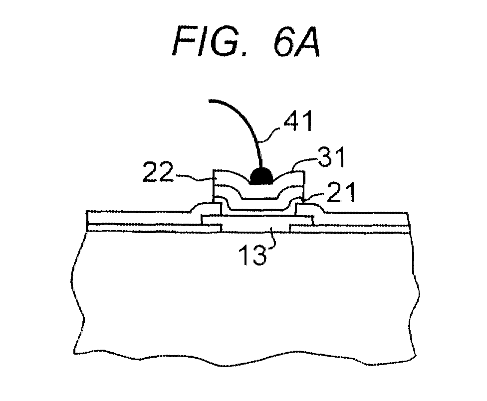
- the bond site to be wire bonded, i.e. 31, is shown in Fig. 6A with gold wire bond 41 attached.
- the wire is preferably gold, or a gold alloy with small amounts of metal additives, such as Au-Be, for hardening etc.
- the diameter of the wire is typically 0.5-2 mils, and preferably 1-1.2 mils.
- the area of the aluminum bond pads is typically in the range 1000-40000 ⁇ m 2 and preferably 5000-25000 ⁇ m 2
- the wire bonding step is a conventional thermocompression operation using bonding using tools widely available in the technology.
- the bond force may be 15-60 grams, preferably 40-60 grams.
- the ultrasonic frequency is in the range 40-200 kHz, preferably 60-120 kHz, and the power in the range 20-200 mW, preferably 50-100 mW. These parameters are suitable for a variety of bonding tools including, e.g. K & S wire bonders.
- the solder bond site 32 is shown with solder bump 42 in Fig. 6B.
- the solder bump is formed by any suitable technique such as solder paste, or evaporation. The latter is typically compatible with high lead content solders, e.g. 95PbSn.
- the solder bump may also be formed by electroplating using e.g. the bottom layer of the composite as the cathode. For this sequence the three layer stack is deposited as described above, and the solder bump sites masked. The top layer or layers may be removed leaving the Ti or Cr layer for the cathode. The bottom layer is masked to localize the electrolytic plating process to the solder bump sites. After plating and solder reflow the bottom layer is patterned. High tin or silver based solders are suited for this approach. Alternatively, these solders may be applied by electroless plating.
- solder compositions that can be used successfully in the processes described above here: I II III IV Sn 5 63 95 3.5 Pb 95 37 0 0 Sb 0 0 5 0 Ag 0 0 0 96.5
- III-V photonic integrated circuits typically have GaAs or InP substrates and multilevels of III-V ternary and/or quaternary layers forming the active devices.
- interconnections can in some applications be similar to those used in silicon IC technology.
- circuits also typically operate at very high speeds where copper metallization is distinctly advantageous.
- the metal interconnect levels formed after the first level are usually aluminum, and one to three aluminum levels are typical. Of these one or more, will be substituted with copper as described above.
- the processes described above contemplate the use processing of individual wafers for either wire bonding or solder bump bonding.
- the invention is also applicable to wafers that are both wire bonded and solder bump bonded.
- a single wafer is processed to have both the wire bond pad of the invention and the solder bump bond.
- This is achieved most conveniently by processing the wafer, as described above, to have the first and second layers, i.e. the titanium/chromium layer, and the layer comprising nickel, then selectively depositing copper on the solder bond sites, and selectively depositing aluminum on the wire bond sites. It will be understood that the latter two steps can be done in either sequence.
- the selective deposition step may be accomplished by standard lithography using a subtractive (mask and etch) method, or preferably an additive (lift-off) method. These layers can be deposited on the bond sites specifically, or over blanket regions containing the bond sites. This approach illustrates profoundly the versatility of having a common composite to solve the copper migration problem for both interconnection strategies.
- This common composite barrier layer is also useful for gold metallization.
- Gold is widely used as an interconnect material in photonic integrated circuits.
- the versatility offered by having a common under bump metallization for a variety of applications will be apparent to those skilled in the art.
Landscapes
- Internal Circuitry In Semiconductor Integrated Circuit Devices (AREA)
- Wire Bonding (AREA)
Abstract
Description
| I | II | III | IV | |
| Sn | 5 | 63 | 95 | 3.5 |
| Pb | 95 | 37 | 0 | 0 |
| Sb | 0 | 0 | 5 | 0 |
| Ag | 0 | 0 | 0 | 96.5 |
Claims (20)
- A method for the manufacture of a semiconductor integrated circuit comprising:(a) depositing a first layer on selected portions of the semiconductor integrated circuit, the first layer being of a material selected from the group consisting of titanium and chromium,(b) depositing a second layer comprising nickel on the first layer,(c) depositing a third layer comprising aluminum on the second layer,(d) etching the first, second, and third layers to form a bond pad, and(e) bonding a conductive wire interconnection to the third layer.
- The method of claim 1 wherein the semiconductor of the semiconductor integrated circuit is silicon.
- The method of claim 2 wherein the wire comprises gold and is bonded using thermocompression bonding.
- The method of claim 1 comprising the additional steps, prior to step (a), of depositing a capping layer on said top interconnection level, forming windows in said capping layer, and proceeding with steps (a) through (c).
- The method of claim 1 wherein the first, second and third layers are sequentially sputtered in the same sputtering apparatus without breaking vacuum.
- The method of claim 1 wherein the nickel layer comprises nickel with 0.5-10% vanadium.
- The method of claim 1 wherein the first layer comprises chromium and is deposited by sputtering in a nitrogen atmosphere.
- The method of claim 1 wherein the semiconductor integrated circuit has a top interconnection level comprising copper.
- The method of claim 1 wherein the semiconductor integrated circuit has a top interconnection level comprising gold.
- A method for the manufacture of a semiconductor integrated circuit comprising:(a) depositing a first layer on selected portions of the semiconductor integrated circuit, the first layer being of a material selected from the group consisting of titanium and chromium,(b) depositing a second layer comprising nickel on the first layer,(c) depositing a third layer comprising copper on the second layer,(d) etching the first, second, and third layers to form a bond pad, and(e) bonding a solder bump interconnection to the third layer.
- The method of claim 10 wherein the semiconductor of the semiconductor integrated circuit is silicon.
- The method of claim 10 wherein the first, second and third layers are sequentially sputtered in the same sputtering apparatus without breaking vacuum.
- The method of claim 10 wherein the nickel layer comprises nickel with 0.5-10% vanadium.
- The method of claim 10 wherein the semiconductor integrated circuit has a top interconnection level comprising copper.
- The method of claim 10 wherein the top interconnection level of the semiconductor integrated circuit comprises gold.
- A method for the manufacture of semiconductor integrated circuits comprising the steps of:(a) forming a copper interconnection layer on a semiconductor substrate,(b) depositing a dielectric layer on said copper interconnection layer,(c) forming a plurality of openings in said dielectric layer to leave exposed portions of said copper interconnection layer,(d) sputtering a first layer on the dielectric layer and on the exposed portions of the copper interconnection layer, the first layer comprising a 100-1500 Angstrom titanium layer,(e) sputtering a second layer on the first layer, the second layer comprising a 2000-20,000 Angstrom layer of a nickel/vanadium alloy,(f) sputtering a third layer on the second layer, the third layer comprising an approximately 1-2 micron layer of aluminum,(g) etching away selected portions of said first, second and third layers to leave a bond pad, and(h) thermocompression bonding a conductive wire to said bond pad.
- The method of claim 16 wherein the first layer is sputtered at a temperature in the range 300-450 °C, the second layer is sputtered at a temperature in the range 25-300 °C, and the third layer is sputtered at a temperature in the range 25-200 °C.
- A method for the manufacture of a semiconductor integrated circuit wherein the top interconnection level of the semiconductor integrated circuit is provided with wire bond interconnection sites and solder bump interconnection sites the method comprising:(a) depositing a first layer on selected portions of the top interconnection level, the first layer being of a material selected from the group consisting of titanium and chromium,(b) depositing a second layer comprising nickel on the first layer,(c) selectively depositing a first contact layer comprising aluminum on the wire bond sites,(d) selectively depositing a second contact layer comprising copper on the solder bump sites,(e) etching the first, second, and first and second contact layers to form wire bond pads and solder bump pads,(f) bonding conductive wire interconnections to the wire bond sites, and(g) bonding solder bump interconnections to the solder bump sites.
- The method of claim 18 wherein the top interconnection level of the semiconductor integrated circuit comprises copper.
- The method of claim 18 wherein the top interconnection level of the semiconductor integrated circuit comprises gold.
Applications Claiming Priority (2)
| Application Number | Priority Date | Filing Date | Title |
|---|---|---|---|
| US09/546,037 US6620720B1 (en) | 2000-04-10 | 2000-04-10 | Interconnections to copper IC's |
| US546037 | 2000-04-10 |
Publications (3)
| Publication Number | Publication Date |
|---|---|
| EP1146552A2 true EP1146552A2 (en) | 2001-10-17 |
| EP1146552A3 EP1146552A3 (en) | 2003-04-16 |
| EP1146552B1 EP1146552B1 (en) | 2011-10-05 |
Family
ID=24178596
Family Applications (1)
| Application Number | Title | Priority Date | Filing Date |
|---|---|---|---|
| EP01303322A Expired - Lifetime EP1146552B1 (en) | 2000-04-10 | 2001-04-09 | Interconnections to copper ICs |
Country Status (6)
| Country | Link |
|---|---|
| US (1) | US6620720B1 (en) |
| EP (1) | EP1146552B1 (en) |
| JP (1) | JP2001351940A (en) |
| KR (1) | KR100857727B1 (en) |
| AT (1) | ATE527687T1 (en) |
| TW (1) | TWI223427B (en) |
Cited By (8)
| Publication number | Priority date | Publication date | Assignee | Title |
|---|---|---|---|---|
| US6683383B2 (en) * | 2001-10-18 | 2004-01-27 | Intel Corporation | Wirebond structure and method to connect to a microelectronic die |
| WO2004001837A3 (en) * | 2002-06-25 | 2004-07-08 | Unitive Int Ltd | Methods of forming electronic structures including conductive shunt layers and related structures |
| US7156284B2 (en) | 2000-12-15 | 2007-01-02 | Unitive International Limited | Low temperature methods of bonding components and related structures |
| DE102007046556A1 (en) * | 2007-09-28 | 2009-04-02 | Infineon Technologies Austria Ag | Semiconductor device with copper metallizations |
| US7579694B2 (en) | 2003-02-18 | 2009-08-25 | Unitive International Limited | Electronic devices including offset conductive bumps |
| US7665652B2 (en) | 2001-09-27 | 2010-02-23 | Unitive International Limited | Electronic devices including metallurgy structures for wire and solder bonding |
| US7839000B2 (en) | 2002-06-25 | 2010-11-23 | Unitive International Limited | Solder structures including barrier layers with nickel and/or copper |
| US8357560B2 (en) | 2006-06-14 | 2013-01-22 | Magnachip Semiconductor Ltd. | Package of MEMS device and method for fabricating the same |
Families Citing this family (50)
| Publication number | Priority date | Publication date | Assignee | Title |
|---|---|---|---|---|
| US6495442B1 (en) * | 2000-10-18 | 2002-12-17 | Magic Corporation | Post passivation interconnection schemes on top of the IC chips |
| EP1332654B1 (en) | 2000-11-10 | 2005-01-12 | Unitive Electronics, Inc. | Methods of positioning components using liquid prime movers and related structures |
| US20020086520A1 (en) * | 2001-01-02 | 2002-07-04 | Advanced Semiconductor Engineering Inc. | Semiconductor device having bump electrode |
| US7498196B2 (en) | 2001-03-30 | 2009-03-03 | Megica Corporation | Structure and manufacturing method of chip scale package |
| JP2003031576A (en) * | 2001-07-17 | 2003-01-31 | Nec Corp | Semiconductor device and method of manufacturing the same |
| US6605524B1 (en) * | 2001-09-10 | 2003-08-12 | Taiwan Semiconductor Manufacturing Company | Bumping process to increase bump height and to create a more robust bump structure |
| DE10222909A1 (en) * | 2002-05-22 | 2003-12-04 | Unaxis Balzers Ag | Sputtering process or device for the production of coatings optimized for residual stress |
| US7531898B2 (en) | 2002-06-25 | 2009-05-12 | Unitive International Limited | Non-Circular via holes for bumping pads and related structures |
| US20040007779A1 (en) * | 2002-07-15 | 2004-01-15 | Diane Arbuthnot | Wafer-level method for fine-pitch, high aspect ratio chip interconnect |
| US7279355B2 (en) * | 2003-06-27 | 2007-10-09 | Avago Technologies Ecbuip (Singapore) Pte Ltd | Method for fabricating a packaging device for semiconductor die and semiconductor device incorporating same |
| US7919787B2 (en) * | 2003-06-27 | 2011-04-05 | Avago Technologies Ecbu Ip (Singapore) Pte. Ltd. | Semiconductor device with a light emitting semiconductor die |
| US7256486B2 (en) * | 2003-06-27 | 2007-08-14 | Avago Technologies Ecbu Ip (Singapore) Pte. Ltd. | Packaging device for semiconductor die, semiconductor device incorporating same and method of making same |
| JP2005093571A (en) * | 2003-09-16 | 2005-04-07 | Hitachi Metals Ltd | Thin film wiring layer |
| US6995475B2 (en) * | 2003-09-18 | 2006-02-07 | International Business Machines Corporation | I/C chip suitable for wire bonding |
| US6960831B2 (en) * | 2003-09-25 | 2005-11-01 | International Business Machines Corporation | Semiconductor device having a composite layer in addition to a barrier layer between copper wiring and aluminum bond pad |
| US7005752B2 (en) | 2003-10-20 | 2006-02-28 | Texas Instruments Incorporated | Direct bumping on integrated circuit contacts enabled by metal-to-insulator adhesion |
| WO2005059957A2 (en) * | 2003-12-12 | 2005-06-30 | Great Wall Semiconductor Corporation | Metal interconnect system and method for direct die attachment |
| JP4406300B2 (en) * | 2004-02-13 | 2010-01-27 | 株式会社東芝 | Semiconductor device and manufacturing method thereof |
| US7410833B2 (en) * | 2004-03-31 | 2008-08-12 | International Business Machines Corporation | Interconnections for flip-chip using lead-free solders and having reaction barrier layers |
| JP4696532B2 (en) * | 2004-05-20 | 2011-06-08 | 株式会社デンソー | Power composite integrated semiconductor device and manufacturing method thereof |
| US7262498B2 (en) * | 2004-10-19 | 2007-08-28 | Hewlett-Packard Development Company, L.P. | Assembly with a ring and bonding pads formed of a same material on a substrate |
| EP1693889B1 (en) | 2005-02-16 | 2017-05-24 | Imec | Method to enhance the initiation of film growth |
| US7927933B2 (en) * | 2005-02-16 | 2011-04-19 | Imec | Method to enhance the initiation of film growth |
| US7381634B2 (en) * | 2005-04-13 | 2008-06-03 | Stats Chippac Ltd. | Integrated circuit system for bonding |
| US20070048991A1 (en) * | 2005-08-23 | 2007-03-01 | Taiwan Semiconductor Manufacturing Co., Ltd. | Copper interconnect structures and fabrication method thereof |
| US8319343B2 (en) * | 2005-09-21 | 2012-11-27 | Agere Systems Llc | Routing under bond pad for the replacement of an interconnect layer |
| US7952206B2 (en) * | 2005-09-27 | 2011-05-31 | Agere Systems Inc. | Solder bump structure for flip chip semiconductor devices and method of manufacture therefore |
| US8076779B2 (en) * | 2005-11-08 | 2011-12-13 | Lsi Corporation | Reduction of macro level stresses in copper/low-K wafers |
| US8552560B2 (en) * | 2005-11-18 | 2013-10-08 | Lsi Corporation | Alternate pad structures/passivation inegration schemes to reduce or eliminate IMC cracking in post wire bonded dies during Cu/Low-K BEOL processing |
| US7504728B2 (en) * | 2005-12-09 | 2009-03-17 | Agere Systems Inc. | Integrated circuit having bond pad with improved thermal and mechanical properties |
| US7674701B2 (en) | 2006-02-08 | 2010-03-09 | Amkor Technology, Inc. | Methods of forming metal layers using multi-layer lift-off patterns |
| US7932615B2 (en) | 2006-02-08 | 2011-04-26 | Amkor Technology, Inc. | Electronic devices including solder bumps on compliant dielectric layers |
| JP5162909B2 (en) * | 2006-04-03 | 2013-03-13 | 豊田合成株式会社 | Semiconductor light emitting device |
| DE102006044691B4 (en) * | 2006-09-22 | 2012-06-21 | Infineon Technologies Ag | Method for producing a terminal conductive structure of a component |
| US7521287B2 (en) * | 2006-11-20 | 2009-04-21 | International Business Machines Corporation | Wire and solder bond forming methods |
| US7601628B2 (en) * | 2006-11-20 | 2009-10-13 | International Business Machines Corporation | Wire and solder bond forming methods |
| JP2008159948A (en) * | 2006-12-25 | 2008-07-10 | Rohm Co Ltd | Semiconductor device |
| JP5045336B2 (en) * | 2007-04-16 | 2012-10-10 | 豊田合成株式会社 | Semiconductor light emitting device |
| JP5069051B2 (en) * | 2007-07-13 | 2012-11-07 | Jx日鉱日石金属株式会社 | Nickel alloy sputtering target |
| US7939949B2 (en) | 2007-09-27 | 2011-05-10 | Micron Technology, Inc. | Semiconductor device with copper wirebond sites and methods of making same |
| US7888257B2 (en) * | 2007-10-10 | 2011-02-15 | Agere Systems Inc. | Integrated circuit package including wire bonds |
| KR101360815B1 (en) * | 2007-10-31 | 2014-02-11 | 에이저 시스템즈 엘엘시 | Bond pad support structure for semiconductor device |
| US7829450B2 (en) * | 2007-11-07 | 2010-11-09 | Infineon Technologies Ag | Method of processing a contact pad, method of manufacturing a contact pad, and integrated circuit element |
| US9953940B2 (en) | 2015-06-26 | 2018-04-24 | International Business Machines Corporation | Corrosion resistant aluminum bond pad structure |
| PL232559B1 (en) * | 2017-07-17 | 2019-06-28 | Instytut Tech Elektronowej | Method for producing multi-layered metallization, multi-layered metallization and application of multi-layered metallization |
| JP7305587B2 (en) * | 2020-03-17 | 2023-07-10 | 株式会社東芝 | Semiconductor equipment and inspection equipment |
| WO2023123116A1 (en) | 2021-12-29 | 2023-07-06 | 京东方科技集团股份有限公司 | Circuit board, functional backplane, backlight module, display panel, and display device |
| JP7879172B2 (en) | 2021-12-31 | 2026-06-23 | 京東方科技集團股▲ふん▼有限公司 | Wiring board, functional backplane, and method for manufacturing the same |
| CN117378289A (en) | 2022-04-21 | 2024-01-09 | 京东方科技集团股份有限公司 | Circuit boards, light-emitting substrates, backlight modules, display panels and display devices |
| US12457685B2 (en) | 2022-10-31 | 2025-10-28 | Beijing Boe Technology Development Co., Ltd. | Circuit board, light-emitting substrate, backlight module, and display apparatus |
Citations (2)
| Publication number | Priority date | Publication date | Assignee | Title |
|---|---|---|---|---|
| US4661375A (en) | 1985-04-22 | 1987-04-28 | At&T Technologies, Inc. | Method for increasing the height of solder bumps |
| US5420073A (en) | 1993-01-08 | 1995-05-30 | International Business Machines Corporation | Structure and method for a superbarrier to prevent diffusion between a noble and a non-noble metal |
Family Cites Families (13)
| Publication number | Priority date | Publication date | Assignee | Title |
|---|---|---|---|---|
| JPS5384466A (en) * | 1976-12-29 | 1978-07-25 | Matsushita Electric Ind Co Ltd | Manufacture of semiconductor device |
| US4330329A (en) * | 1979-11-28 | 1982-05-18 | Tanaka Denshi Kogyo Kabushiki Kaisha | Gold bonding wire for semiconductor elements and the semiconductor element |
| US5169680A (en) * | 1987-05-07 | 1992-12-08 | Intel Corporation | Electroless deposition for IC fabrication |
| US5508229A (en) * | 1994-05-24 | 1996-04-16 | National Semiconductor Corporation | Method for forming solder bumps in semiconductor devices |
| JPH08204250A (en) * | 1995-01-20 | 1996-08-09 | Asahi Chem Ind Co Ltd | Semiconductor device |
| US5755859A (en) * | 1995-08-24 | 1998-05-26 | International Business Machines Corporation | Cobalt-tin alloys and their applications for devices, chip interconnections and packaging |
| JP2882380B2 (en) * | 1996-09-05 | 1999-04-12 | 日本電気株式会社 | Semiconductor device and manufacturing method thereof |
| TW459323B (en) * | 1996-12-04 | 2001-10-11 | Seiko Epson Corp | Manufacturing method for semiconductor device |
| US6441487B2 (en) * | 1997-10-20 | 2002-08-27 | Flip Chip Technologies, L.L.C. | Chip scale package using large ductile solder balls |
| US6875681B1 (en) * | 1997-12-31 | 2005-04-05 | Intel Corporation | Wafer passivation structure and method of fabrication |
| JP2943805B1 (en) * | 1998-09-17 | 1999-08-30 | 日本電気株式会社 | Semiconductor device and manufacturing method thereof |
| US6187680B1 (en) * | 1998-10-07 | 2001-02-13 | International Business Machines Corporation | Method/structure for creating aluminum wirebound pad on copper BEOL |
| US6281106B1 (en) * | 1999-11-25 | 2001-08-28 | Delphi Technologies, Inc. | Method of solder bumping a circuit component |
-
2000
- 2000-04-10 US US09/546,037 patent/US6620720B1/en not_active Expired - Lifetime
-
2001
- 2001-04-09 AT AT01303322T patent/ATE527687T1/en not_active IP Right Cessation
- 2001-04-09 KR KR1020010018579A patent/KR100857727B1/en not_active Expired - Lifetime
- 2001-04-09 TW TW090108450A patent/TWI223427B/en not_active IP Right Cessation
- 2001-04-09 EP EP01303322A patent/EP1146552B1/en not_active Expired - Lifetime
- 2001-04-10 JP JP2001110719A patent/JP2001351940A/en active Pending
Patent Citations (2)
| Publication number | Priority date | Publication date | Assignee | Title |
|---|---|---|---|---|
| US4661375A (en) | 1985-04-22 | 1987-04-28 | At&T Technologies, Inc. | Method for increasing the height of solder bumps |
| US5420073A (en) | 1993-01-08 | 1995-05-30 | International Business Machines Corporation | Structure and method for a superbarrier to prevent diffusion between a noble and a non-noble metal |
Cited By (12)
| Publication number | Priority date | Publication date | Assignee | Title |
|---|---|---|---|---|
| US7156284B2 (en) | 2000-12-15 | 2007-01-02 | Unitive International Limited | Low temperature methods of bonding components and related structures |
| US7665652B2 (en) | 2001-09-27 | 2010-02-23 | Unitive International Limited | Electronic devices including metallurgy structures for wire and solder bonding |
| US6683383B2 (en) * | 2001-10-18 | 2004-01-27 | Intel Corporation | Wirebond structure and method to connect to a microelectronic die |
| US6924554B2 (en) * | 2001-10-18 | 2005-08-02 | Intel Corporation | Wirebond structure and method to connect to a microelectronic die |
| CN100380647C (en) * | 2001-10-18 | 2008-04-09 | 英特尔公司 | Wire bonding structure and microelectronic circuit chip and connection method thereof |
| US7393772B2 (en) | 2001-10-18 | 2008-07-01 | Intel Corporation | Wirebond structure and method to connect to a microelectronic die |
| WO2004001837A3 (en) * | 2002-06-25 | 2004-07-08 | Unitive Int Ltd | Methods of forming electronic structures including conductive shunt layers and related structures |
| US7839000B2 (en) | 2002-06-25 | 2010-11-23 | Unitive International Limited | Solder structures including barrier layers with nickel and/or copper |
| US7579694B2 (en) | 2003-02-18 | 2009-08-25 | Unitive International Limited | Electronic devices including offset conductive bumps |
| US8357560B2 (en) | 2006-06-14 | 2013-01-22 | Magnachip Semiconductor Ltd. | Package of MEMS device and method for fabricating the same |
| DE102007046556A1 (en) * | 2007-09-28 | 2009-04-02 | Infineon Technologies Austria Ag | Semiconductor device with copper metallizations |
| US10347580B2 (en) | 2007-09-28 | 2019-07-09 | Infineon Technologies Austria Ag | Semiconductor component comprising copper metallizations |
Also Published As
| Publication number | Publication date |
|---|---|
| KR20010090777A (en) | 2001-10-19 |
| US6620720B1 (en) | 2003-09-16 |
| ATE527687T1 (en) | 2011-10-15 |
| EP1146552B1 (en) | 2011-10-05 |
| TWI223427B (en) | 2004-11-01 |
| JP2001351940A (en) | 2001-12-21 |
| KR100857727B1 (en) | 2008-09-10 |
| EP1146552A3 (en) | 2003-04-16 |
Similar Documents
| Publication | Publication Date | Title |
|---|---|---|
| US6620720B1 (en) | Interconnections to copper IC's | |
| US6750133B2 (en) | Selective ball-limiting metallurgy etching processes for fabrication of electroplated tin bumps | |
| KR100213152B1 (en) | Electroplated solder terminal and its fabrication method | |
| US7427557B2 (en) | Methods of forming bumps using barrier layers as etch masks | |
| US6417089B1 (en) | Method of forming solder bumps with reduced undercutting of under bump metallurgy (UBM) | |
| US8580679B2 (en) | Designs and methods for conductive bumps | |
| US7932169B2 (en) | Interconnection for flip-chip using lead-free solders and having improved reaction barrier layers | |
| CN1096110C (en) | Solder bump structure containing titanium barrier layer and method of forming same | |
| US8003512B2 (en) | Structure of UBM and solder bumps and methods of fabrication | |
| US7098126B2 (en) | Formation of electroplate solder on an organic circuit board for flip chip joints and board to board solder joints | |
| CN110783298B (en) | Semiconductor device and manufacturing method thereof | |
| US20120012642A1 (en) | Interconnections for flip-chip using lead-free solders and having reaction barrier layers | |
| US20020086520A1 (en) | Semiconductor device having bump electrode | |
| KR100476301B1 (en) | Fabrication Method of multilayer UBM by Electroplating for Flip chip Interconnections | |
| JP5064632B2 (en) | Method and apparatus for forming an interconnect structure | |
| US12315834B2 (en) | Electroplated indium bump stacks for cryogenic electronics | |
| EP1322146A1 (en) | Method of electroplating solder bumps on an organic circuit board | |
| CN100421216C (en) | Etching solution and method for manufacturing conductive bump by selectively removing barrier layer by using same | |
| HK1093380B (en) | Microelectronic apparatus including conductive bumps and method thereof |
Legal Events
| Date | Code | Title | Description |
|---|---|---|---|
| PUAI | Public reference made under article 153(3) epc to a published international application that has entered the european phase |
Free format text: ORIGINAL CODE: 0009012 |
|
| AK | Designated contracting states |
Kind code of ref document: A2 Designated state(s): AT BE CH CY DE DK ES FI FR GB GR IE IT LI LU MC NL PT SE TR |
|
| AX | Request for extension of the european patent |
Free format text: AL;LT;LV;MK;RO;SI |
|
| PUAL | Search report despatched |
Free format text: ORIGINAL CODE: 0009013 |
|
| AK | Designated contracting states |
Designated state(s): AT BE CH CY DE DK ES FI FR GB GR IE IT LI LU MC NL PT SE TR |
|
| AX | Request for extension of the european patent |
Extension state: AL LT LV MK RO SI |
|
| RIC1 | Information provided on ipc code assigned before grant |
Ipc: 7H 01L 21/60 A Ipc: 7H 01L 23/485 B Ipc: 7H 01L 23/532 B |
|
| 17P | Request for examination filed |
Effective date: 20031015 |
|
| AKX | Designation fees paid |
Designated state(s): AT BE CH CY DE DK ES FI FR GB GR IE IT LI LU MC NL PT SE TR |
|
| 17Q | First examination report despatched |
Effective date: 20040617 |
|
| 17Q | First examination report despatched |
Effective date: 20040617 |
|
| GRAP | Despatch of communication of intention to grant a patent |
Free format text: ORIGINAL CODE: EPIDOSNIGR1 |
|
| GRAS | Grant fee paid |
Free format text: ORIGINAL CODE: EPIDOSNIGR3 |
|
| GRAA | (expected) grant |
Free format text: ORIGINAL CODE: 0009210 |
|
| AK | Designated contracting states |
Kind code of ref document: B1 Designated state(s): AT BE CH CY DE DK ES FI FR GB GR IE IT LI LU MC NL PT SE TR |
|
| REG | Reference to a national code |
Ref country code: GB Ref legal event code: FG4D |
|
| REG | Reference to a national code |
Ref country code: CH Ref legal event code: EP Ref country code: DE Ref legal event code: R081 Ref document number: 60145418 Country of ref document: DE Owner name: AVAGO TECHNOLOGIES GENERAL IP (SINGAPORE) PTE., SG Free format text: FORMER OWNER: AGERE SYSTEMS GUARDIAN CORP., MIAMI LAKES, FLA., US |
|
| REG | Reference to a national code |
Ref country code: IE Ref legal event code: FG4D |
|
| REG | Reference to a national code |
Ref country code: DE Ref legal event code: R096 Ref document number: 60145418 Country of ref document: DE Effective date: 20111208 |
|
| REG | Reference to a national code |
Ref country code: NL Ref legal event code: VDEP Effective date: 20111005 |
|
| REG | Reference to a national code |
Ref country code: AT Ref legal event code: MK05 Ref document number: 527687 Country of ref document: AT Kind code of ref document: T Effective date: 20111005 |
|
| PG25 | Lapsed in a contracting state [announced via postgrant information from national office to epo] |
Ref country code: BE Free format text: LAPSE BECAUSE OF FAILURE TO SUBMIT A TRANSLATION OF THE DESCRIPTION OR TO PAY THE FEE WITHIN THE PRESCRIBED TIME-LIMIT Effective date: 20111005 |
|
| PG25 | Lapsed in a contracting state [announced via postgrant information from national office to epo] |
Ref country code: NL Free format text: LAPSE BECAUSE OF FAILURE TO SUBMIT A TRANSLATION OF THE DESCRIPTION OR TO PAY THE FEE WITHIN THE PRESCRIBED TIME-LIMIT Effective date: 20111005 Ref country code: GR Free format text: LAPSE BECAUSE OF FAILURE TO SUBMIT A TRANSLATION OF THE DESCRIPTION OR TO PAY THE FEE WITHIN THE PRESCRIBED TIME-LIMIT Effective date: 20120106 Ref country code: SE Free format text: LAPSE BECAUSE OF FAILURE TO SUBMIT A TRANSLATION OF THE DESCRIPTION OR TO PAY THE FEE WITHIN THE PRESCRIBED TIME-LIMIT Effective date: 20111005 |
|
| PG25 | Lapsed in a contracting state [announced via postgrant information from national office to epo] |
Ref country code: CY Free format text: LAPSE BECAUSE OF FAILURE TO SUBMIT A TRANSLATION OF THE DESCRIPTION OR TO PAY THE FEE WITHIN THE PRESCRIBED TIME-LIMIT Effective date: 20111005 |
|
| PG25 | Lapsed in a contracting state [announced via postgrant information from national office to epo] |
Ref country code: DK Free format text: LAPSE BECAUSE OF FAILURE TO SUBMIT A TRANSLATION OF THE DESCRIPTION OR TO PAY THE FEE WITHIN THE PRESCRIBED TIME-LIMIT Effective date: 20111005 |
|
| PLBE | No opposition filed within time limit |
Free format text: ORIGINAL CODE: 0009261 |
|
| STAA | Information on the status of an ep patent application or granted ep patent |
Free format text: STATUS: NO OPPOSITION FILED WITHIN TIME LIMIT |
|
| PG25 | Lapsed in a contracting state [announced via postgrant information from national office to epo] |
Ref country code: IT Free format text: LAPSE BECAUSE OF FAILURE TO SUBMIT A TRANSLATION OF THE DESCRIPTION OR TO PAY THE FEE WITHIN THE PRESCRIBED TIME-LIMIT Effective date: 20111005 |
|
| 26N | No opposition filed |
Effective date: 20120706 |
|
| REG | Reference to a national code |
Ref country code: DE Ref legal event code: R097 Ref document number: 60145418 Country of ref document: DE Effective date: 20120706 |
|
| PG25 | Lapsed in a contracting state [announced via postgrant information from national office to epo] |
Ref country code: MC Free format text: LAPSE BECAUSE OF NON-PAYMENT OF DUE FEES Effective date: 20120430 |
|
| REG | Reference to a national code |
Ref country code: CH Ref legal event code: PL |
|
| REG | Reference to a national code |
Ref country code: IE Ref legal event code: MM4A |
|
| PG25 | Lapsed in a contracting state [announced via postgrant information from national office to epo] |
Ref country code: AT Free format text: LAPSE BECAUSE OF FAILURE TO SUBMIT A TRANSLATION OF THE DESCRIPTION OR TO PAY THE FEE WITHIN THE PRESCRIBED TIME-LIMIT Effective date: 20111005 Ref country code: LI Free format text: LAPSE BECAUSE OF NON-PAYMENT OF DUE FEES Effective date: 20120430 Ref country code: IE Free format text: LAPSE BECAUSE OF NON-PAYMENT OF DUE FEES Effective date: 20120409 Ref country code: CH Free format text: LAPSE BECAUSE OF NON-PAYMENT OF DUE FEES Effective date: 20120430 |
|
| PG25 | Lapsed in a contracting state [announced via postgrant information from national office to epo] |
Ref country code: ES Free format text: LAPSE BECAUSE OF FAILURE TO SUBMIT A TRANSLATION OF THE DESCRIPTION OR TO PAY THE FEE WITHIN THE PRESCRIBED TIME-LIMIT Effective date: 20120116 |
|
| PG25 | Lapsed in a contracting state [announced via postgrant information from national office to epo] |
Ref country code: FI Free format text: LAPSE BECAUSE OF FAILURE TO SUBMIT A TRANSLATION OF THE DESCRIPTION OR TO PAY THE FEE WITHIN THE PRESCRIBED TIME-LIMIT Effective date: 20111005 |
|
| PG25 | Lapsed in a contracting state [announced via postgrant information from national office to epo] |
Ref country code: TR Free format text: LAPSE BECAUSE OF FAILURE TO SUBMIT A TRANSLATION OF THE DESCRIPTION OR TO PAY THE FEE WITHIN THE PRESCRIBED TIME-LIMIT Effective date: 20111005 |
|
| PG25 | Lapsed in a contracting state [announced via postgrant information from national office to epo] |
Ref country code: LU Free format text: LAPSE BECAUSE OF NON-PAYMENT OF DUE FEES Effective date: 20120409 |
|
| PG25 | Lapsed in a contracting state [announced via postgrant information from national office to epo] |
Ref country code: PT Free format text: LAPSE BECAUSE OF FAILURE TO SUBMIT A TRANSLATION OF THE DESCRIPTION OR TO PAY THE FEE WITHIN THE PRESCRIBED TIME-LIMIT Effective date: 20111005 |
|
| REG | Reference to a national code |
Ref country code: FR Ref legal event code: PLFP Year of fee payment: 15 |
|
| PGFP | Annual fee paid to national office [announced via postgrant information from national office to epo] |
Ref country code: GB Payment date: 20150324 Year of fee payment: 15 Ref country code: FR Payment date: 20150319 Year of fee payment: 15 |
|
| REG | Reference to a national code |
Ref country code: DE Ref legal event code: R082 Ref document number: 60145418 Country of ref document: DE Representative=s name: DILG, HAEUSLER, SCHINDELMANN PATENTANWALTSGESE, DE Ref country code: DE Ref legal event code: R082 Ref document number: 60145418 Country of ref document: DE Representative=s name: DILG HAEUSLER SCHINDELMANN PATENTANWALTSGESELL, DE Ref country code: DE Ref legal event code: R081 Ref document number: 60145418 Country of ref document: DE Owner name: AVAGO TECHNOLOGIES GENERAL IP (SINGAPORE) PTE., SG Free format text: FORMER OWNER: AGERE SYSTEMS GUARDIAN CORP., MIAMI LAKES, FLA., US Ref country code: DE Ref legal event code: R081 Ref document number: 60145418 Country of ref document: DE Owner name: AVAGO TECHNOLOGIES INTERNATIONAL SALES PTE. LI, SG Free format text: FORMER OWNER: AGERE SYSTEMS GUARDIAN CORP., MIAMI LAKES, FLA., US |
|
| GBPC | Gb: european patent ceased through non-payment of renewal fee |
Effective date: 20160409 |
|
| REG | Reference to a national code |
Ref country code: FR Ref legal event code: ST Effective date: 20161230 |
|
| PG25 | Lapsed in a contracting state [announced via postgrant information from national office to epo] |
Ref country code: FR Free format text: LAPSE BECAUSE OF NON-PAYMENT OF DUE FEES Effective date: 20160502 Ref country code: GB Free format text: LAPSE BECAUSE OF NON-PAYMENT OF DUE FEES Effective date: 20160409 |
|
| REG | Reference to a national code |
Ref country code: DE Ref legal event code: R081 Ref document number: 60145418 Country of ref document: DE Owner name: AVAGO TECHNOLOGIES INTERNATIONAL SALES PTE. LI, SG Free format text: FORMER OWNER: AVAGO TECHNOLOGIES GENERAL IP (SINGAPORE) PTE. LTD., SINGAPORE, SG Ref country code: DE Ref legal event code: R082 Ref document number: 60145418 Country of ref document: DE Representative=s name: DILG, HAEUSLER, SCHINDELMANN PATENTANWALTSGESE, DE Ref country code: DE Ref legal event code: R082 Ref document number: 60145418 Country of ref document: DE Representative=s name: DILG HAEUSLER SCHINDELMANN PATENTANWALTSGESELL, DE |
|
| PGFP | Annual fee paid to national office [announced via postgrant information from national office to epo] |
Ref country code: DE Payment date: 20200319 Year of fee payment: 20 |
|
| REG | Reference to a national code |
Ref country code: DE Ref legal event code: R071 Ref document number: 60145418 Country of ref document: DE |