EP1141930B1 - Method and apparatus for implementing dynamic display memory - Google Patents
Method and apparatus for implementing dynamic display memory Download PDFInfo
- Publication number
- EP1141930B1 EP1141930B1 EP00913225A EP00913225A EP1141930B1 EP 1141930 B1 EP1141930 B1 EP 1141930B1 EP 00913225 A EP00913225 A EP 00913225A EP 00913225 A EP00913225 A EP 00913225A EP 1141930 B1 EP1141930 B1 EP 1141930B1
- Authority
- EP
- European Patent Office
- Prior art keywords
- graphics
- memory
- operand
- address
- cpu
- Prior art date
- Legal status (The legal status is an assumption and is not a legal conclusion. Google has not performed a legal analysis and makes no representation as to the accuracy of the status listed.)
- Expired - Lifetime
Links
Images


Classifications
-
- G—PHYSICS
- G09—EDUCATION; CRYPTOGRAPHY; DISPLAY; ADVERTISING; SEALS
- G09G—ARRANGEMENTS OR CIRCUITS FOR CONTROL OF INDICATING DEVICES USING STATIC MEANS TO PRESENT VARIABLE INFORMATION
- G09G5/00—Control arrangements or circuits for visual indicators common to cathode-ray tube indicators and other visual indicators
- G09G5/36—Control arrangements or circuits for visual indicators common to cathode-ray tube indicators and other visual indicators characterised by the display of a graphic pattern, e.g. using an all-points-addressable [APA] memory
- G09G5/363—Graphics controllers
-
- G—PHYSICS
- G09—EDUCATION; CRYPTOGRAPHY; DISPLAY; ADVERTISING; SEALS
- G09G—ARRANGEMENTS OR CIRCUITS FOR CONTROL OF INDICATING DEVICES USING STATIC MEANS TO PRESENT VARIABLE INFORMATION
- G09G5/00—Control arrangements or circuits for visual indicators common to cathode-ray tube indicators and other visual indicators
- G09G5/36—Control arrangements or circuits for visual indicators common to cathode-ray tube indicators and other visual indicators characterised by the display of a graphic pattern, e.g. using an all-points-addressable [APA] memory
- G09G5/39—Control of the bit-mapped memory
- G09G5/393—Arrangements for updating the contents of the bit-mapped memory
-
- G—PHYSICS
- G09—EDUCATION; CRYPTOGRAPHY; DISPLAY; ADVERTISING; SEALS
- G09G—ARRANGEMENTS OR CIRCUITS FOR CONTROL OF INDICATING DEVICES USING STATIC MEANS TO PRESENT VARIABLE INFORMATION
- G09G2360/00—Aspects of the architecture of display systems
- G09G2360/12—Frame memory handling
- G09G2360/122—Tiling
Definitions
- the invention relates generally to graphics systems and more specifically to a system for and a method of management of graphics memory.
- a graphics subsystem which can control its own memory, and such subsytems are typically connected to a CPU, main memory, and other devices such as auxiliary storage devices by way of a system bus.
- a system bus would be connected to the CPU, main memory, and other devices. This allows the CPU access to everything connected to the bus.
- Graphics subsystems often include high speed memory only accessible through the graphics subsystem. Additionally, such subsystems often may access operands in main memory, typically over the system bus.
- a CPU will often have to perform operations on graphics operands.
- the organization of these operands will be controlled by the graphics subsystem. This requires that the CPU get the operands from the graphics subsystem.
- the CPU or an associated memory management unit (MMU) may control the organization of graphics operands, in which case the graphics subsystem must get data from the CPU or MMU in order to operate. In either case, some level of inefficiency is introduced, as one device must request data from the other device in order to perform its tasks.
- both the CPU and the graphics subsystem will control organization of the graphics operands.
- the CPU and the graphics subsystem will not need to request operands from each other, they will need to inform each other of when graphics operands are moved in memory or otherwise made inaccessible.
- increased overhead is introduced into every operation on a graphics operand.
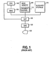
- FIG. 1 illustrates a prior art system. It includes Graphics Address Transformer 100 (GAT 100) connected to Graphics Device Controller 120 (GDC 120) which in turn is connected to Graphics Device 130. GAT 100 is also connected to a bus which connects it to Main Memory 160, Auxiliary Storage 170 and Memory Management Unit 150 (MMU 150). Central Processing Unit 140 (CPU 140) is connected to MMU 150 and thereby accesses Main Memory 160 and Auxiliary Storage 170: CPU 140 also has a control connection to GAT 100 which allows CPU 140 to control GAT 100. Main Memory 160 includes Segment Buffer 110.
- GAT 100 Graphics Address Transformer 100
- GDC 120 Graphics Device Controller 120
- MMU 150 Memory Management Unit 150
- CPU 140 Central Processing Unit 140
- CPU 140 Central Processing Unit 140
- CPU 140 also has a control connection to GAT 100 which allows CPU 140 to control GAT 100.
- Main Memory 160 includes Segment Buffer 110.
- CPU 140 operates on graphics operands stored in Main Memory 160 and Auxiliary Storage 170.
- MMU 150 manages Main Memory 160 and Auxiliary Storage 170, maintaining records of where various operands are stored. When operands are moved within memory, MMU 150 updates its records of the operands locations.
- GDC 120 also operates on graphics operands stored in Main Memory 160 and Auxiliary Storage 170.
- GAT 100 maintains records of where graphics operands are stored and updates these records when operands are moved within memory. As a result, whenever CPU 140 or GDC 120 perform an action that results in movement of graphics operands, the records of both MMU 150 and GAT 100 must be updated. Maintaining coherency between the records of MMU 150 and GAT 100 requires highly synchronized operations, as many errors can be encountered in accessing either Main Memory 160 or Auxiliary Storage 110.
- CPU 140 may move a segment of memory from Auxiliary Storage 170 to Segment Buffer 110 of Main Memory 140, thereby overwriting the former contents of Segment Buffer 110. If such an action occurs, MMU 150 will update its records, thereby keeping track of what operands are in Segment Buffer 110, and what operands that were in Segment Buffer 110 are no longer there, If any of these operands are graphics operands, then CPU 140 must exert control over GAT 100, forcing GAT 100 to update its records concerning the various graphics operands involved. Furthermore, if GDC 120 was accessing Segment Buffer 110 when CPU 140 overwrote Segment Buffer 110, GDC 120 may now be operating on corrupted data or incorrect data.
- Figure 1 is a prior art graphics display system.
- Figure 2 illustrates one embodiment of a system.
- Figure 3 is a flowchart illustrating a possible mode of operation of a system.
- Figure 4 illustrates another embodiment of a system.
- Figure 5 is a flowchart illustrating a possible mode of operation of a system.
- Figure 6 illustrates an alternative embodiment of a system.
- Figure 7 illustrates a tiled memory
- Figure 8 illustrates memory access within a system.
- the present invention allows for improved processing of graphics operands and elimination of overhead processing in any system utilizing graphics data.
- a method and apparatus for implementing dynamic display memory is described.
- numerous specific details are set forth in order to provide a thorough understanding of the invention. It will be apparent, however, to one skilled in the art that the invention can be practiced without these specific details. In other instances, structures and devices are shown in block diagram form in order to avoid obscuring the invention.
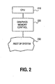
- FIG. 2 illustrates one example of a system.
- CPU 210 is a central processing unit and is well known in the art
- Graphics Memory Control 220 is coupled to CPU 210 and to the Rest of the system 230.
- Graphics Memory Control 220 embodies logic sufficient to track the location of graphics operands in memory located in Rest of system 230 and to convert virtual addresses of graphics operands from CPU 210 into system addresses suitable for use by Rest of system 230.
- Graphics Memory Control 220 determines whether the operand in question is a graphics operand. If it is, Graphics Memory Control 220 determines what system memory address corresponds to the virtual address presented by CPU 210. Graphics Memory Control 220 then accesses the operand in question within Rest of system 230 utilizing the appropriate system address and completes the access for CPU 210.
- Graphics Memory Control 220 allows Rest of system 230 to respond appropriately to the memory access by CPU 210. Such a response would be well known in the art, and includes but is not limited to completing the memory access, signaling an error, or transforming the virtual address to a corresponding physical address and thereby accessing the operand.
- CPU accesses to memory would include read and write accesses, and completion of such accesses typically includes either writing the operand to the appropriate location or reading the operand from the appropriate location.
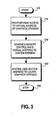
- the apparatus of Figure 2 can be further understood by reference to Figure 3 .
- the process of Figure 3 begins with Initiation step 300 and proceeds to CPU Access step 310.
- CPU Access step 310 involves CPU 210 accessing a graphics operand by performing a memory access to a location based on its virtual address.
- the process proceeds to Graphics Mapping step 320, where Graphics Memory Control 220 maps or otherwise transforms the virtual address supplied by CPU 210 to a system address or other address suitable for use within Rest of system 230.
- the process then proceeds to System Access step 330 where Rest of system 230 performs the appropriate memory access using the system address to locate the graphics operand, and the process terminates with Termination step 340.
- FIG. 2 could represent CPU 210 and Graphics Memory Control 220 as separate components. However, it could also represent CPU 210 and Graphics Memory Control 220 as parts of a single integrated circuit.
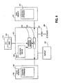
- CPU 410 contains MMU 420 and is coupled to a memory controller, referred to in this embodiment as a memory control hub (MCH) 430.
- MCH 430 contains Graphics Device 440, Address Reorder Stage 450 and GTT 460 (a Graphics Translation Table).
- MCH 430 is coupled to Local Memory 480, Main Memory 470, Display 490, and I/O Devices 496.
- Local Memory 480 contains Graphics Operands 485, and Main Memory 470 contains Graphics Operands 475.
- MCH 430 is coupled through I/O Bus 493 to I/O Devices 496.
- Both Graphics Device 440 and CPU 410 have access to Address Reorder Stage 450.
- only CPU 410 can modify GTT 460, so only CPU 410 can change the location in memory of graphics operands.
- CPU Access step 510 represents CPU 410 performing an access to the virtual address of a graphics operand.
- MMU processing step 520 represents MMU 420 mapping or otherwise transforming the virtual address supplied by CPU 410 to a system address suitable for use in accessing memory outside of CPU 410. Note that if the graphics operand accessed by CPU 410 were contained in a cache within CPU 410 then MMU 420 might not have accessed memory outside of CPU 410. However, most graphics operands will be uncacheable, so the memory access will go outside the CPU.
- MCH 430 checks whether the system address from MMU 420 is within the Graphics Memory range.
- the Graphics Memory range is the range of addresses that is mapped by GTT 460 for use by Graphics Device 440. If the system address is not within the Graphics Memory range, the process proceeds to Access step 540 where MCH 430 performs the memory access at the system address in a normal fashion. Typically this would entail some sort of address translation, determination of whether the address led to a particular memory device, and an access of that particular device.
- Address Reorder Stage 450 determines whether the address is within a fenced region.
- Address Reorder Stage 450 includes fence registers which contain information delimiting certain portions of the memory assigned for use by Address Reorder Stage 450 as fenced regions. These fenced regions may be organized in a different manner from other memory or otherwise vary in some way from the rest of system memory. In one embodiment, the contents of the fenced region may be tiled or otherwise reorganized, meaning that memory as associated with graphics operands may be ordered to form tiles that mimic logically a spatial form such as a rectangle, square, solid, or other shape. If the system address is determined to be within a fenced region, appropriate reordering of the system address is performed at Reordering step 560. Such reordering typically involves some simple mathematical recalculation and may also be performed through use of a lookup table.
- the reordered address is mapped to a physical address at Mapping step 570.
- the system address as supplied by MMU 420 is mapped to a physical address at Mapping step 570.
- This mapping step typically involves use of a translation table, in this case GTT 460 the Graphics Translation Table, which contains entries indicating what addresses or ranges of system addresses correspond to particular locations in main or local memory. Similar translation tables would be used by MCH 430 in performing the memory access of Access step 540.
- the translated address is used to perform an access at Access step 580 in a fashion similar to that of Access step 540. The process terminates with Termination step 590.
- FIG. 6 illustrates yet another embodiment of a system.
- CPU 610 includes MMU 620 and is coupled to Memory Control 630.
- Memory Control 630 includes Graphics Memory Control 640 and is coupled to Bus 660. Also coupled to Bus 660 are Local Memory 650, System Memory 690, Input Device 680 and Output Device 670.
- Memory Control 630 can translate the address supplied by CPU 610 and access the operand on Bus 660 in any of the other components coupled to Bus 660. If the operand is a graphics operand, Graphics Memory Control 640 appropriately manipulates and transforms the address supplied by CPU 610 to perform the same kind of access as that described for Memory Control 630.
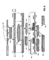
- Figure 8 illustrates an example of a system and how a graphics operand is accessed.
- Graphics Operand Virtual Addresses 805 are the addresses seen by programs executing on a CPU.
- MMU 810 is the internal memory management unit of the CPU. It transforms virtual addresses to system addresses through use of a lookup table containing entries indicating which virtual addresses correspond to which system addresses.
- Memory Range 815 is the structure of memory mapped to by MMU 810, and each system address for a graphics operand which MMU 810 produces addresses some part of this memory space. The portion shown is the graphics memory accessible to the CPU and other portions of the memory range would correspond to devices such as input or other output devices.
- Graphics Memory Space 825 is the structure of graphics memory as seen by a graphics device. Graphics Device Access 820 shows that the graphics device accesses the memory without the offset N used by the CPU and MMU 810 in accessing the graphics memory space as the graphics device does not have access to the rest of the memory accessible to the CPU. Both Memory Range 815 and Memory Space 825 are linear in nature, as this is the structure necessary for programs operating on a CPU and for access by the graphics device (for example they could be 64MB in size).
- Address Reorder stage 835 When Graphics Device Access 820 presents an address, or the MMU 810 presents a system address for access to memory, Address Reorder stage 835 operates on that address. Address Reorder stage 835 determines whether the address presented is within one of the fenced regions by checking it against the contents of Fence Registers 830. If the address is within a fenced region, Address Reorder stage 835 then transforms the address based on other information in Fence Registers 830 which specifies how memory in Reordered Address Space 840 is organized. Reordered Address Space 840 can have memory organized in different manners to optimize transfer rates between memory and the CPU or the graphics device. Two manners of organization are linear organization and tiled organization. Linearly organized address spaces such as Linear space 843, 849, and 858 all have addresses that each come one after another in memory from the point of view of Address Reorder Stage 835.
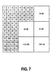
- Tiled addresses such as those in Tiled spaces 846, 852, and 855, would be arranged in a manner as shown in Figure 7 , where each tile has addresses counting across locations within the tile row by row, and the overall structure has each address in a given tile before all addresses in the next tile and after all addresses in the previous tile.
- tiles are restricted to 2kB in size and tiled spaces must have a width (measured in tiles) that is a power of two.
- the pitch referred to in Tiled spaces 846, 852, and 855 is the width of the Tiled spaces.
- not all addresses within a tile need to correspond to an actual operand, so the addresses in Tiled spaces 846, 852, and 855 that are marked by an X need not correspond to actual operands. Additionally, such unneeded tiles may also correspond to a scratch memory page.
- tiles could be designed with other sizes, shapes and constraints, and addresses within tiles could be ordered in ways other than that depicted in Figure 7 .
- Tiled spaces can be useful because they may be shaped and sized for optimum or near-optimum utilization of system resources in transferring graphics operands between memory and either the graphics device or the CPU. Their shapes would then be designed to correspond to graphics objects or surfaces. Understandably, tiled spaces may be allocated and deallocated dynamically during operation of the system. Ordering of addresses within tiled spaces may be done in a variety of ways, including the row-major (X-axis) order of Figure 7 , but also including column-major (Y-axis) order and other ordering methods.
- GTLB 860 Graphics Translation Lookaside Buffer
- GTT 865 Graphics Translation Table
- GTT 865 itself is typically stored in System Memory 870 in one embodiment, and need not be stored within a portion of System Memory 870 allocated to addresses within Graphics Memory Space 825.
- GTLB 860 and GTT 865 take the form of lookup tables associating a set of addresses with a set of locations in System Memory 870 or Local Memory 875 in one embodiment.
- a TLB or Translation Table may be implemented in a variety of ways.
- GTLB 860 and GTT 865 differ from other TLBs and Translation Tables because they are dedicated to use by the graphics device and can only be used to associate addresses for graphics operands with memory. This constraint is not imposed by the components of GTLB 860 or GTT 865, rather it is imposed by the system design encompassing GTLB 860 and GTT 865.
- GTLB 860 is profitably included in a memory control hub, and GTT 865 is accessible through that memory control hub.
- System Memory 870 typically represents the random access memory of a system, but could also represent other forms of storage.
- Local Memory 875 typically represents memory dedicated for use with the graphics device, and need not be present in order for the system to function.
Landscapes
- Engineering & Computer Science (AREA)
- Physics & Mathematics (AREA)
- Computer Hardware Design (AREA)
- General Physics & Mathematics (AREA)
- Theoretical Computer Science (AREA)
- Computer Graphics (AREA)
- Memory System Of A Hierarchy Structure (AREA)
- Image Input (AREA)
- Image Processing (AREA)
Description
- The invention relates generally to graphics systems and more specifically to a system for and a method of management of graphics memory.
- It is generally well known e.g. from
WO95/15528 - In such systems, a CPU will often have to perform operations on graphics operands. However, the organization of these operands will be controlled by the graphics subsystem. This requires that the CPU get the operands from the graphics subsystem. Alternatively, the CPU or an associated memory management unit (MMU) may control the organization of graphics operands, in which case the graphics subsystem must get data from the CPU or MMU in order to operate. In either case, some level of inefficiency is introduced, as one device must request data from the other device in order to perform its tasks. -
- In other systems, both the CPU and the graphics subsystem will control organization of the graphics operands. In these systems, while the CPU and the graphics subsystem will not need to request operands from each other, they will need to inform each other of when graphics operands are moved in memory or otherwise made inaccessible. As a result, increased overhead is introduced into every operation on a graphics operand.
-
Figure 1 illustrates a prior art system. It includes Graphics Address Transformer 100 (GAT 100) connected to Graphics Device Controller 120 (GDC 120) which in turn is connected toGraphics Device 130. GAT 100 is also connected to a bus which connects it toMain Memory 160,Auxiliary Storage 170 and Memory Management Unit 150 (MMU 150). Central Processing Unit 140 (CPU 140) is connected to MMU 150 and thereby accessesMain Memory 160 and Auxiliary Storage 170:CPU 140 also has a control connection toGAT 100 which allowsCPU 140 to controlGAT 100.Main Memory 160 includesSegment Buffer 110. -
CPU 140 operates on graphics operands stored inMain Memory 160 andAuxiliary Storage 170. To facilitate this, MMU 150 managesMain Memory 160 andAuxiliary Storage 170, maintaining records of where various operands are stored. When operands are moved within memory, MMU 150 updates its records of the operands locations. GDC 120 also operates on graphics operands stored inMain Memory 160 andAuxiliary Storage 170. To facilitate this, GAT 100 maintains records of where graphics operands are stored and updates these records when operands are moved within memory. As a result, wheneverCPU 140 or GDC 120 perform an action that results in movement of graphics operands, the records of both MMU 150 and GAT 100 must be updated. Maintaining coherency between the records of MMU 150 and GAT 100 requires highly synchronized operations, as many errors can be encountered in accessing eitherMain Memory 160 orAuxiliary Storage 110. - For example,
CPU 140 may move a segment of memory fromAuxiliary Storage 170 toSegment Buffer 110 ofMain Memory 140, thereby overwriting the former contents ofSegment Buffer 110. If such an action occurs, MMU 150 will update its records, thereby keeping track of what operands are inSegment Buffer 110, and what operands that were inSegment Buffer 110 are no longer there, If any of these operands are graphics operands, thenCPU 140 must exert control overGAT 100, forcing GAT 100 to update its records concerning the various graphics operands involved. Furthermore, if GDC 120 was accessingSegment Buffer 110 whenCPU 140overwrote Segment Buffer 110, GDC 120 may now be operating on corrupted data or incorrect data. - According to a first aspect of this invention there is provided a system as claimed in
claim 1 herein. - According to a second aspect of this invention there is provided a method as claimed in
claim 7 herein. - The present invention is illustrated by way of example and not limitation in the accompanying figures.
-
Figure 1 is a prior art graphics display system. -
Figure 2 illustrates one embodiment of a system. -
Figure 3 is a flowchart illustrating a possible mode of operation of a system. -
Figure 4 illustrates another embodiment of a system. -
Figure 5 is a flowchart illustrating a possible mode of operation of a system. -
Figure 6 illustrates an alternative embodiment of a system. -
Figure 7 illustrates a tiled memory. -
Figure 8 illustrates memory access within a system. - The present invention allows for improved processing of graphics operands and elimination of overhead processing in any system utilizing graphics data. A method and apparatus for implementing dynamic display memory is described. In the following description, for purposes of explanation, numerous specific details are set forth in order to provide a thorough understanding of the invention. It will be apparent, however, to one skilled in the art that the invention can be practiced without these specific details. In other instances, structures and devices are shown in block diagram form in order to avoid obscuring the invention.
- Reference in the specification to "one embodiment" or "an embodiment" means that a particular feature, structure, or characteristic described in connection with the embodiment is included in at least one embodiment of the invention. The appearances of the phrase "in one embodiment" in various places in the specification are not necessarily all referring to the same embodiment.
-
Figure 2 illustrates one example of a system.CPU 210 is a central processing unit and is well known in the art Graphics Memory Control 220 is coupled toCPU 210 and to the Rest of thesystem 230.Graphics Memory Control 220 embodies logic sufficient to track the location of graphics operands in memory located in Rest ofsystem 230 and to convert virtual addresses of graphics operands fromCPU 210 into system addresses suitable for use by Rest ofsystem 230. Thus, whenCPU 210 accesses an operand,Graphics Memory Control 220 determines whether the operand in question is a graphics operand. If it is, Graphics Memory Control 220 determines what system memory address corresponds to the virtual address presented byCPU 210. Graphics Memory Control 220 then accesses the operand in question within Rest ofsystem 230 utilizing the appropriate system address and completes the access forCPU 210. - If the operand is determined not to be a graphics operand, then
Graphics Memory Control 220 allows Rest ofsystem 230 to respond appropriately to the memory access byCPU 210. Such a response would be well known in the art, and includes but is not limited to completing the memory access, signaling an error, or transforming the virtual address to a corresponding physical address and thereby accessing the operand. CPU accesses to memory would include read and write accesses, and completion of such accesses typically includes either writing the operand to the appropriate location or reading the operand from the appropriate location. - The apparatus of
Figure 2 can be further understood by reference toFigure 3 . The process ofFigure 3 begins withInitiation step 300 and proceeds toCPU Access step 310. CPU Accessstep 310 involvesCPU 210 accessing a graphics operand by performing a memory access to a location based on its virtual address. The process proceeds toGraphics Mapping step 320, whereGraphics Memory Control 220 maps or otherwise transforms the virtual address supplied byCPU 210 to a system address or other address suitable for use within Rest ofsystem 230. The process then proceeds toSystem Access step 330 where Rest ofsystem 230 performs the appropriate memory access using the system address to locate the graphics operand, and the process terminates withTermination step 340. - As will be apparent to one skilled in the art, the block diagram of
Figure 2 could representCPU 210 andGraphics Memory Control 220 as separate components. However, it could also representCPU 210 andGraphics Memory Control 220 as parts of a single integrated circuit. - Turning to
Figure 4 , an embodiment of a system is illustrated. InFigure 4 ,CPU 410 containsMMU 420 and is coupled to a memory controller, referred to in this embodiment as a memory control hub (MCH) 430.MCH 430 containsGraphics Device 440,Address Reorder Stage 450 and GTT 460 (a Graphics Translation Table).MCH 430 is coupled toLocal Memory 480,Main Memory 470,Display 490, and I/O Devices 496.Local Memory 480 containsGraphics Operands 485, andMain Memory 470 containsGraphics Operands 475.MCH 430 is coupled through I/O Bus 493 to I/O Devices 496. BothGraphics Device 440 andCPU 410 have access toAddress Reorder Stage 450. Preferably, for coherency reasons,only CPU 410 can modifyGTT 460, soonly CPU 410 can change the location in memory of graphics operands. - Operation of the system of
Figure 4 can be better understood with reference to the method of operation illustrated inFigure 5 .CPU Access step 510 representsCPU 410 performing an access to the virtual address of a graphics operand.MMU processing step 520 representsMMU 420 mapping or otherwise transforming the virtual address supplied byCPU 410 to a system address suitable for use in accessing memory outside ofCPU 410. Note that if the graphics operand accessed byCPU 410 were contained in a cache withinCPU 410 thenMMU 420 might not have accessed memory outside ofCPU 410. However, most graphics operands will be uncacheable, so the memory access will go outside the CPU. - At
determination step 530,MCH 430 checks whether the system address fromMMU 420 is within the Graphics Memory range. The Graphics Memory range is the range of addresses that is mapped byGTT 460 for use byGraphics Device 440. If the system address is not within the Graphics Memory range, the process proceeds toAccess step 540 whereMCH 430 performs the memory access at the system address in a normal fashion. Typically this would entail some sort of address translation, determination of whether the address led to a particular memory device, and an access of that particular device. - If the system address is within the Graphics Memory range, the process proceeds to
determination step 550, where theAddress Reorder Stage 450 determines whether the address is within a fenced region. One embodiment ofAddress Reorder Stage 450 includes fence registers which contain information delimiting certain portions of the memory assigned for use byAddress Reorder Stage 450 as fenced regions. These fenced regions may be organized in a different manner from other memory or otherwise vary in some way from the rest of system memory. In one embodiment, the contents of the fenced region may be tiled or otherwise reorganized, meaning that memory as associated with graphics operands may be ordered to form tiles that mimic logically a spatial form such as a rectangle, square, solid, or other shape. If the system address is determined to be within a fenced region, appropriate reordering of the system address is performed atReordering step 560. Such reordering typically involves some simple mathematical recalculation and may also be performed through use of a lookup table. - After
Reordering step 560, the reordered address is mapped to a physical address atMapping step 570. Likewise, if no reordering was necessary, the system address as supplied byMMU 420 is mapped to a physical address atMapping step 570. This mapping step typically involves use of a translation table, in thiscase GTT 460 the Graphics Translation Table, which contains entries indicating what addresses or ranges of system addresses correspond to particular locations in main or local memory. Similar translation tables would be used byMCH 430 in performing the memory access ofAccess step 540. Finally, the translated address is used to perform an access atAccess step 580 in a fashion similar to that ofAccess step 540. The process terminates withTermination step 590. -
Figure 6 illustrates yet another embodiment of a system.CPU 610 includesMMU 620 and is coupled toMemory Control 630.Memory Control 630 includesGraphics Memory Control 640 and is coupled toBus 660. Also coupled toBus 660 areLocal Memory 650,System Memory 690,Input Device 680 andOutput Device 670. AfterCPU 610 requests access to an operand,Memory Control 630 can translate the address supplied byCPU 610 and access the operand onBus 660 in any of the other components coupled toBus 660. If the operand is a graphics operand,Graphics Memory Control 640 appropriately manipulates and transforms the address supplied byCPU 610 to perform the same kind of access as that described forMemory Control 630. -
Figure 8 illustrates an example of a system and how a graphics operand is accessed. Graphics OperandVirtual Addresses 805 are the addresses seen by programs executing on a CPU.MMU 810 is the internal memory management unit of the CPU. It transforms virtual addresses to system addresses through use of a lookup table containing entries indicating which virtual addresses correspond to which system addresses.Memory Range 815 is the structure of memory mapped to byMMU 810, and each system address for a graphics operand whichMMU 810 produces addresses some part of this memory space. The portion shown is the graphics memory accessible to the CPU and other portions of the memory range would correspond to devices such as input or other output devices. -
Graphics Memory Space 825 is the structure of graphics memory as seen by a graphics device.Graphics Device Access 820 shows that the graphics device accesses the memory without the offset N used by the CPU andMMU 810 in accessing the graphics memory space as the graphics device does not have access to the rest of the memory accessible to the CPU. BothMemory Range 815 andMemory Space 825 are linear in nature, as this is the structure necessary for programs operating on a CPU and for access by the graphics device (for example they could be 64MB in size). - When
Graphics Device Access 820 presents an address, or theMMU 810 presents a system address for access to memory, Address Reorder stage 835 operates on that address. Address Reorder stage 835 determines whether the address presented is within one of the fenced regions by checking it against the contents of Fence Registers 830. If the address is within a fenced region, Address Reorder stage 835 then transforms the address based on other information inFence Registers 830 which specifies how memory inReordered Address Space 840 is organized.Reordered Address Space 840 can have memory organized in different manners to optimize transfer rates between memory and the CPU or the graphics device. Two manners of organization are linear organization and tiled organization. Linearly organized address spaces such asLinear space - Tiled addresses, such as those in
Tiled spaces Figure 7 , where each tile has addresses counting across locations within the tile row by row, and the overall structure has each address in a given tile before all addresses in the next tile and after all addresses in the previous tile. In one embodiment, tiles are restricted to 2kB in size and tiled spaces must have a width (measured in tiles) that is a power of two. The pitch referred to inTiled spaces Tiled spaces Figure 7 . - Tiled spaces can be useful because they may be shaped and sized for optimum or near-optimum utilization of system resources in transferring graphics operands between memory and either the graphics device or the CPU. Their shapes would then be designed to correspond to graphics objects or surfaces. Understandably, tiled spaces may be allocated and deallocated dynamically during operation of the system. Ordering of addresses within tiled spaces may be done in a variety of ways, including the row-major (X-axis) order of
Figure 7 , but also including column-major (Y-axis) order and other ordering methods. - Returning to
Figure 8 , accesses to addresses inReordered Address Space 840 go through GTLB 860 (Graphics Translation Lookaside Buffer) in concert with GTT 865 (Graphics Translation Table).GTT 865 itself is typically stored inSystem Memory 870 in one embodiment, and need not be stored within a portion ofSystem Memory 870 allocated to addresses withinGraphics Memory Space 825.GTLB 860 andGTT 865 take the form of lookup tables associating a set of addresses with a set of locations inSystem Memory 870 orLocal Memory 875 in one embodiment. As is well known in the art, a TLB or Translation Table may be implemented in a variety of ways. However,GTLB 860 andGTT 865 differ from other TLBs and Translation Tables because they are dedicated to use by the graphics device and can only be used to associate addresses for graphics operands with memory. This constraint is not imposed by the components ofGTLB 860 orGTT 865, rather it is imposed by the systemdesign encompassing GTLB 860 andGTT 865.GTLB 860 is profitably included in a memory control hub, andGTT 865 is accessible through that memory control hub. -
System Memory 870 typically represents the random access memory of a system, but could also represent other forms of storage.Local Memory 875 typically represents memory dedicated for use with the graphics device, and need not be present in order for the system to function.
Claims (11)
- A system comprising:a central processor (410, 610);a local memory (480, 650);a system memory (470, 690); anda memory controller (430, 630) coupled to the central processor and coupled to both the local memory and the system memory, characterised in that the memory controller comprises a graphics control component (640) adapted to determine whether an operand accessed by the central processor is a graphics operand by determining whether a system address of the graphics operand is within a graphics memory range, the graphics control component being adapted to transform an address of the operand to an address corresponding to a location of the operand in one of the local memory or the system memory if the operand is a graphics operand.
- The system of claim 1 further comprising a graphics translation table to be used by the graphics memory control component to locate the graphics operands in either of the local memory or the system memory, the graphics translation table having a set of one or more entries that may be modified by the central processor, wherein each entry of the set of entries is configured to associate a virtual address to a system address, the system address being suitable as the location of an operand in one of the local memory or the system memory.
- The system of claim 2, wherein the graphics translation table is stored in the local memory.
- The system of claim 2 or 3, wherein the graphics translation table is stored in one of the local memory or the system memory.
- The system of any preceding claim, wherein the local memory is configured for the storage of graphics operands.
- The system of claim 4 further comprising:a set of fence registers to be maintained by the graphics memory control component, the set of fence registers being adapted to store information defining the organisation of locations of graphics operands in either the local memory or the system memory; whereinthe graphics memory control component has an address reorder component, the address reorder component being adapted to utilise the set of fence registers in order to determine which system address corresponds to the virtual address of a graphics operand.
- A method of accessing memory comprising:a central processor accessing an operand at a virtual address; anda memory control component determining if the operand is a graphics operand;the method comprising the steps of
if the operand is a graphics operand, then mapping the virtual address to a system address that corresponds to the virtual address and accessing the operand at the system address in of a local memory or a system memory; and
if the operand is not a graphics operand, then responding to the accessing. - The method of claim 7, wherein the graphics operand is in a tiled memory space.
- The method of claim 7, wherein mapping the virtual address to the system address comprises utilising an entry from a graphics translation table having a set of one or more entries.
- The method of claim 9 further comprising altering the set of entries of the graphics translation table by a central processor.
- The method of claim 7 further comprising determining whether the graphics operand is located within a linear memory space or a tiled memory space.
Applications Claiming Priority (3)
| Application Number | Priority Date | Filing Date | Title |
|---|---|---|---|
| US231609 | 1999-01-15 | ||
| US09/231,609 US6362826B1 (en) | 1999-01-15 | 1999-01-15 | Method and apparatus for implementing dynamic display memory |
| PCT/US2000/000776 WO2000042594A1 (en) | 1999-01-15 | 2000-01-12 | Method and apparatus for implementing dynamic display memory |
Publications (2)
| Publication Number | Publication Date |
|---|---|
| EP1141930A1 EP1141930A1 (en) | 2001-10-10 |
| EP1141930B1 true EP1141930B1 (en) | 2008-05-14 |
Family
ID=22869956
Family Applications (1)
| Application Number | Title | Priority Date | Filing Date |
|---|---|---|---|
| EP00913225A Expired - Lifetime EP1141930B1 (en) | 1999-01-15 | 2000-01-12 | Method and apparatus for implementing dynamic display memory |
Country Status (10)
| Country | Link |
|---|---|
| US (2) | US6362826B1 (en) |
| EP (1) | EP1141930B1 (en) |
| JP (1) | JP4562919B2 (en) |
| KR (1) | KR100433499B1 (en) |
| CN (1) | CN1135477C (en) |
| AU (1) | AU3470700A (en) |
| DE (1) | DE60038871D1 (en) |
| HK (1) | HK1038091A1 (en) |
| TW (1) | TWI250482B (en) |
| WO (1) | WO2000042594A1 (en) |
Families Citing this family (39)
| Publication number | Priority date | Publication date | Assignee | Title |
|---|---|---|---|---|
| US6545684B1 (en) * | 1999-12-29 | 2003-04-08 | Intel Corporation | Accessing data stored in a memory |
| US6538650B1 (en) * | 2000-01-10 | 2003-03-25 | Intel Corporation | Efficient TLB entry management for the render operands residing in the tiled memory |
| US7710425B1 (en) * | 2000-06-09 | 2010-05-04 | 3Dlabs Inc. Ltd. | Graphic memory management with invisible hardware-managed page faulting |
| US6704021B1 (en) * | 2000-11-20 | 2004-03-09 | Ati International Srl | Method and apparatus for efficiently processing vertex information in a video graphics system |
| US6795079B2 (en) * | 2001-02-15 | 2004-09-21 | Sony Corporation | Two-dimensional buffer pages |
| US7379069B2 (en) | 2001-02-15 | 2008-05-27 | Sony Corporation | Checkerboard buffer using two-dimensional buffer pages |
| US6803917B2 (en) | 2001-02-15 | 2004-10-12 | Sony Corporation | Checkerboard buffer using memory bank alternation |
| US7205993B2 (en) * | 2001-02-15 | 2007-04-17 | Sony Corporation | Checkerboard buffer using two-dimensional buffer pages and using memory bank alternation |
| US6828977B2 (en) * | 2001-02-15 | 2004-12-07 | Sony Corporation | Dynamic buffer pages |
| US7038691B2 (en) * | 2001-02-15 | 2006-05-02 | Sony Corporation | Two-dimensional buffer pages using memory bank alternation |
| US20030058368A1 (en) * | 2001-09-24 | 2003-03-27 | Mark Champion | Image warping using pixel pages |
| US9058292B2 (en) | 2004-12-29 | 2015-06-16 | Intel Corporation | System and method for one step address translation of graphics addresses in virtualization |
| US7444583B2 (en) * | 2005-05-27 | 2008-10-28 | Microsoft Corporation | Standard graphics specification and data binding |
| US7512752B2 (en) | 2005-05-31 | 2009-03-31 | Broadcom Corporation | Systems, methods, and apparatus for pixel fetch request interface |
| US7831780B2 (en) * | 2005-06-24 | 2010-11-09 | Nvidia Corporation | Operating system supplemental disk caching system and method |
| US7616218B1 (en) * | 2005-12-05 | 2009-11-10 | Nvidia Corporation | Apparatus, system, and method for clipping graphics primitives |
| US8593474B2 (en) * | 2005-12-30 | 2013-11-26 | Intel Corporation | Method and system for symmetric allocation for a shared L2 mapping cache |
| US8352709B1 (en) | 2006-09-19 | 2013-01-08 | Nvidia Corporation | Direct memory access techniques that include caching segmentation data |
| US8601223B1 (en) * | 2006-09-19 | 2013-12-03 | Nvidia Corporation | Techniques for servicing fetch requests utilizing coalesing page table entries |
| US8347064B1 (en) | 2006-09-19 | 2013-01-01 | Nvidia Corporation | Memory access techniques in an aperture mapped memory space |
| US8543792B1 (en) | 2006-09-19 | 2013-09-24 | Nvidia Corporation | Memory access techniques including coalesing page table entries |
| US7840732B2 (en) * | 2006-09-25 | 2010-11-23 | Honeywell International Inc. | Stacked card address assignment |
| US8700883B1 (en) | 2006-10-24 | 2014-04-15 | Nvidia Corporation | Memory access techniques providing for override of a page table |
| US8707011B1 (en) | 2006-10-24 | 2014-04-22 | Nvidia Corporation | Memory access techniques utilizing a set-associative translation lookaside buffer |
| US8533425B1 (en) | 2006-11-01 | 2013-09-10 | Nvidia Corporation | Age based miss replay system and method |
| US8607008B1 (en) | 2006-11-01 | 2013-12-10 | Nvidia Corporation | System and method for independent invalidation on a per engine basis |
| US8504794B1 (en) | 2006-11-01 | 2013-08-06 | Nvidia Corporation | Override system and method for memory access management |
| US8347065B1 (en) * | 2006-11-01 | 2013-01-01 | Glasco David B | System and method for concurrently managing memory access requests |
| US8706975B1 (en) | 2006-11-01 | 2014-04-22 | Nvidia Corporation | Memory access management block bind system and method |
| US8700865B1 (en) | 2006-11-02 | 2014-04-15 | Nvidia Corporation | Compressed data access system and method |
| US20080276067A1 (en) * | 2007-05-01 | 2008-11-06 | Via Technologies, Inc. | Method and Apparatus for Page Table Pre-Fetching in Zero Frame Display Channel |
| US8719547B2 (en) * | 2009-09-18 | 2014-05-06 | Intel Corporation | Providing hardware support for shared virtual memory between local and remote physical memory |
| US10146545B2 (en) | 2012-03-13 | 2018-12-04 | Nvidia Corporation | Translation address cache for a microprocessor |
| US9880846B2 (en) | 2012-04-11 | 2018-01-30 | Nvidia Corporation | Improving hit rate of code translation redirection table with replacement strategy based on usage history table of evicted entries |
| US10241810B2 (en) | 2012-05-18 | 2019-03-26 | Nvidia Corporation | Instruction-optimizing processor with branch-count table in hardware |
| US20140189310A1 (en) | 2012-12-27 | 2014-07-03 | Nvidia Corporation | Fault detection in instruction translations |
| US10108424B2 (en) | 2013-03-14 | 2018-10-23 | Nvidia Corporation | Profiling code portions to generate translations |
| US20140365930A1 (en) * | 2013-06-10 | 2014-12-11 | Hewlett-Packard Development Company, L.P. | Remote display of content elements |
| KR101751629B1 (en) * | 2014-12-24 | 2017-06-27 | 인텔 코포레이션 | Hybrid on-demand graphics translation table shadowing |
Family Cites Families (20)
| Publication number | Priority date | Publication date | Assignee | Title |
|---|---|---|---|---|
| JPH01181163A (en) | 1988-01-13 | 1989-07-19 | Seiko Instr & Electron Ltd | Graphic display system |
| JP3350043B2 (en) * | 1990-07-27 | 2002-11-25 | 株式会社日立製作所 | Graphic processing apparatus and graphic processing method |
| US5313577A (en) * | 1991-08-21 | 1994-05-17 | Digital Equipment Corporation | Translation of virtual addresses in a computer graphics system |
| JP2966182B2 (en) * | 1992-03-12 | 1999-10-25 | 株式会社日立製作所 | Computer system |
| US5450542A (en) * | 1993-11-30 | 1995-09-12 | Vlsi Technology, Inc. | Bus interface with graphics and system paths for an integrated memory system |
| WO1995015528A1 (en) | 1993-11-30 | 1995-06-08 | Vlsi Technology, Inc. | A reallocatable memory subsystem enabling transparent transfer of memory function during upgrade |
| JPH0850573A (en) * | 1994-08-04 | 1996-02-20 | Hitachi Ltd | Microcomputer |
| US5854637A (en) * | 1995-08-17 | 1998-12-29 | Intel Corporation | Method and apparatus for managing access to a computer system memory shared by a graphics controller and a memory controller |
| US5758177A (en) * | 1995-09-11 | 1998-05-26 | Advanced Microsystems, Inc. | Computer system having separate digital and analog system chips for improved performance |
| US6104417A (en) * | 1996-09-13 | 2000-08-15 | Silicon Graphics, Inc. | Unified memory computer architecture with dynamic graphics memory allocation |
| JPH10222459A (en) * | 1997-02-10 | 1998-08-21 | Hitachi Ltd | Function memory and data processor using the same |
| EP0884715A1 (en) | 1997-06-12 | 1998-12-16 | Hewlett-Packard Company | Single-chip chipset with integrated graphics controller |
| US6052133A (en) * | 1997-06-27 | 2000-04-18 | S3 Incorporated | Multi-function controller and method for a computer graphics display system |
| US6266753B1 (en) * | 1997-07-10 | 2001-07-24 | Cirrus Logic, Inc. | Memory manager for multi-media apparatus and method therefor |
| US5914730A (en) * | 1997-09-09 | 1999-06-22 | Compaq Computer Corp. | System and method for invalidating and updating individual GART table entries for accelerated graphics port transaction requests |
| US6157398A (en) * | 1997-12-30 | 2000-12-05 | Micron Technology, Inc. | Method of implementing an accelerated graphics port for a multiple memory controller computer system |
| US6097402A (en) * | 1998-02-10 | 2000-08-01 | Intel Corporation | System and method for placement of operands in system memory |
| US6477623B2 (en) * | 1998-10-23 | 2002-11-05 | Micron Technology, Inc. | Method for providing graphics controller embedded in a core logic unit |
| US6145039A (en) * | 1998-11-03 | 2000-11-07 | Intel Corporation | Method and apparatus for an improved interface between computer components |
| US6326973B1 (en) * | 1998-12-07 | 2001-12-04 | Compaq Computer Corporation | Method and system for allocating AGP/GART memory from the local AGP memory controller in a highly parallel system architecture (HPSA) |
-
1999
- 1999-01-15 US US09/231,609 patent/US6362826B1/en not_active Expired - Lifetime
-
2000
- 2000-01-12 EP EP00913225A patent/EP1141930B1/en not_active Expired - Lifetime
- 2000-01-12 WO PCT/US2000/000776 patent/WO2000042594A1/en active IP Right Grant
- 2000-01-12 AU AU34707/00A patent/AU3470700A/en not_active Abandoned
- 2000-01-12 JP JP2000594101A patent/JP4562919B2/en not_active Expired - Fee Related
- 2000-01-12 CN CNB008026513A patent/CN1135477C/en not_active Expired - Fee Related
- 2000-01-12 DE DE60038871T patent/DE60038871D1/en not_active Expired - Lifetime
- 2000-01-12 KR KR10-2001-7008948A patent/KR100433499B1/en not_active IP Right Cessation
- 2000-01-25 TW TW089100589A patent/TWI250482B/en not_active IP Right Cessation
-
2001
- 2001-11-05 US US09/993,217 patent/US6650332B2/en not_active Expired - Lifetime
- 2001-11-09 HK HK01107885A patent/HK1038091A1/en not_active IP Right Cessation
Also Published As
| Publication number | Publication date |
|---|---|
| JP2002535763A (en) | 2002-10-22 |
| TWI250482B (en) | 2006-03-01 |
| CN1135477C (en) | 2004-01-21 |
| US6362826B1 (en) | 2002-03-26 |
| AU3470700A (en) | 2000-08-01 |
| EP1141930A1 (en) | 2001-10-10 |
| US6650332B2 (en) | 2003-11-18 |
| WO2000042594A9 (en) | 2002-03-28 |
| CN1347545A (en) | 2002-05-01 |
| HK1038091A1 (en) | 2002-03-01 |
| DE60038871D1 (en) | 2008-06-26 |
| JP4562919B2 (en) | 2010-10-13 |
| KR100433499B1 (en) | 2004-05-31 |
| US20020075271A1 (en) | 2002-06-20 |
| KR20020013832A (en) | 2002-02-21 |
| WO2000042594A1 (en) | 2000-07-20 |
Similar Documents
| Publication | Publication Date | Title |
|---|---|---|
| EP1141930B1 (en) | Method and apparatus for implementing dynamic display memory | |
| US7149872B2 (en) | System and method for identifying TLB entries associated with a physical address of a specified range | |
| US7777752B2 (en) | Method of implementing an accelerated graphics port for a multiple memory controller computer system | |
| US6204863B1 (en) | Method for dynamic XY tiled texture caching | |
| US8451281B2 (en) | Shared virtual memory between a host and discrete graphics device in a computing system | |
| US6195734B1 (en) | System for implementing a graphic address remapping table as a virtual register file in system memory | |
| US6252612B1 (en) | Accelerated graphics port for multiple memory controller computer system | |
| EP1988467A1 (en) | Virtual memory translation with pre-fetch prediction | |
| US7925836B2 (en) | Selective coherency control | |
| CN112631961B (en) | Memory management unit, address translation method and processor | |
| JP2017045457A (en) | Transaction-based hybrid memory module, and method of operating the same | |
| WO1992022867A1 (en) | Improving computer performance by simulated cache associativity | |
| US6633299B1 (en) | Method and apparatus for implementing smart allocation policies for a small frame buffer cache serving 3D and 2D streams | |
| US5293622A (en) | Computer system with input/output cache | |
| US20040117590A1 (en) | Aliasing support for a data processing system having no system memory | |
| CA2313257C (en) | Accelerated graphics port for multiple memory controller computer system | |
| EP0745941A2 (en) | A system and method for providing a flexible memory hierarchy | |
| US20040117583A1 (en) | Apparatus for influencing process scheduling in a data processing system capable of utilizing a virtual memory processing scheme | |
| CA2140961C (en) | Dual paged apertures | |
| WO1998014877A1 (en) | Virtual addressing for subsystem dma | |
| JPH0659975A (en) | Cache memory device for frame buffer | |
| JPH02226447A (en) | Computer system and memory access therefor | |
| JPH10105466A (en) | Cache memory control method for disk device | |
| JPH04326437A (en) | Information processor | |
| JPH11184456A (en) | Method and device for plotting displaying and navigation system |
Legal Events
| Date | Code | Title | Description |
|---|---|---|---|
| PUAI | Public reference made under article 153(3) epc to a published international application that has entered the european phase |
Free format text: ORIGINAL CODE: 0009012 |
|
| 17P | Request for examination filed |
Effective date: 20010705 |
|
| AK | Designated contracting states |
Kind code of ref document: A1 Designated state(s): AT BE CH CY DE DK ES FI FR GB GR IE IT LI LU MC NL PT SE |
|
| 17Q | First examination report despatched |
Effective date: 20021213 |
|
| RBV | Designated contracting states (corrected) |
Designated state(s): DE FR GB |
|
| RIC1 | Information provided on ipc code assigned before grant |
Ipc: 7G 09G 5/39 A |
|
| GRAP | Despatch of communication of intention to grant a patent |
Free format text: ORIGINAL CODE: EPIDOSNIGR1 |
|
| GRAS | Grant fee paid |
Free format text: ORIGINAL CODE: EPIDOSNIGR3 |
|
| GRAA | (expected) grant |
Free format text: ORIGINAL CODE: 0009210 |
|
| AK | Designated contracting states |
Kind code of ref document: B1 Designated state(s): DE FR GB |
|
| REG | Reference to a national code |
Ref country code: GB Ref legal event code: FG4D |
|
| REF | Corresponds to: |
Ref document number: 60038871 Country of ref document: DE Date of ref document: 20080626 Kind code of ref document: P |
|
| REG | Reference to a national code |
Ref country code: HK Ref legal event code: GR Ref document number: 1038091 Country of ref document: HK |
|
| PLBE | No opposition filed within time limit |
Free format text: ORIGINAL CODE: 0009261 |
|
| STAA | Information on the status of an ep patent application or granted ep patent |
Free format text: STATUS: NO OPPOSITION FILED WITHIN TIME LIMIT |
|
| 26N | No opposition filed |
Effective date: 20090217 |
|
| PGFP | Annual fee paid to national office [announced via postgrant information from national office to epo] |
Ref country code: FR Payment date: 20120130 Year of fee payment: 13 |
|
| REG | Reference to a national code |
Ref country code: FR Ref legal event code: ST Effective date: 20130930 |
|
| PG25 | Lapsed in a contracting state [announced via postgrant information from national office to epo] |
Ref country code: FR Free format text: LAPSE BECAUSE OF NON-PAYMENT OF DUE FEES Effective date: 20130131 |
|
| PGFP | Annual fee paid to national office [announced via postgrant information from national office to epo] |
Ref country code: DE Payment date: 20160105 Year of fee payment: 17 |
|
| PGFP | Annual fee paid to national office [announced via postgrant information from national office to epo] |
Ref country code: GB Payment date: 20160106 Year of fee payment: 17 |
|
| REG | Reference to a national code |
Ref country code: DE Ref legal event code: R119 Ref document number: 60038871 Country of ref document: DE |
|
| GBPC | Gb: european patent ceased through non-payment of renewal fee |
Effective date: 20170112 |
|
| PG25 | Lapsed in a contracting state [announced via postgrant information from national office to epo] |
Ref country code: DE Free format text: LAPSE BECAUSE OF NON-PAYMENT OF DUE FEES Effective date: 20170801 Ref country code: GB Free format text: LAPSE BECAUSE OF NON-PAYMENT OF DUE FEES Effective date: 20170112 |