EP1139658A2 - Amplification type solid-state imaging device and high-speed readout method - Google Patents
Amplification type solid-state imaging device and high-speed readout method Download PDFInfo
- Publication number
- EP1139658A2 EP1139658A2 EP01106500A EP01106500A EP1139658A2 EP 1139658 A2 EP1139658 A2 EP 1139658A2 EP 01106500 A EP01106500 A EP 01106500A EP 01106500 A EP01106500 A EP 01106500A EP 1139658 A2 EP1139658 A2 EP 1139658A2
- Authority
- EP
- European Patent Office
- Prior art keywords
- circuit
- horizontal
- readout
- potential
- charges
- Prior art date
- Legal status (The legal status is an assumption and is not a legal conclusion. Google has not performed a legal analysis and makes no representation as to the accuracy of the status listed.)
- Granted
Links
- 238000003384 imaging method Methods 0.000 title claims abstract description 77
- 238000000034 method Methods 0.000 title claims description 33
- 230000003321 amplification Effects 0.000 title description 6
- 238000003199 nucleic acid amplification method Methods 0.000 title description 6
- 238000003860 storage Methods 0.000 claims abstract description 64
- 238000012545 processing Methods 0.000 claims abstract description 47
- 238000006243 chemical reaction Methods 0.000 claims abstract description 28
- 230000008569 process Effects 0.000 claims description 11
- 230000003213 activating effect Effects 0.000 claims description 10
- 239000004065 semiconductor Substances 0.000 claims description 10
- 239000000758 substrate Substances 0.000 claims description 10
- 238000007599 discharging Methods 0.000 claims description 8
- 238000012935 Averaging Methods 0.000 claims description 7
- 230000010365 information processing Effects 0.000 claims description 6
- 238000012546 transfer Methods 0.000 claims description 6
- 239000003990 capacitor Substances 0.000 description 38
- 238000010276 construction Methods 0.000 description 13
- 230000008878 coupling Effects 0.000 description 9
- 238000010168 coupling process Methods 0.000 description 9
- 238000005859 coupling reaction Methods 0.000 description 9
- 238000010586 diagram Methods 0.000 description 7
- 238000004519 manufacturing process Methods 0.000 description 4
- 238000003379 elimination reaction Methods 0.000 description 3
- 230000008030 elimination Effects 0.000 description 2
- 238000005516 engineering process Methods 0.000 description 2
- 230000010354 integration Effects 0.000 description 2
- 101100421449 Caenorhabditis elegans shn-1 gene Proteins 0.000 description 1
- 230000008859 change Effects 0.000 description 1
- 239000000470 constituent Substances 0.000 description 1
- 238000007796 conventional method Methods 0.000 description 1
- 238000012937 correction Methods 0.000 description 1
- 230000000694 effects Effects 0.000 description 1
- 230000006872 improvement Effects 0.000 description 1
- 230000014759 maintenance of location Effects 0.000 description 1
- 230000009467 reduction Effects 0.000 description 1
- 230000035945 sensitivity Effects 0.000 description 1
Images



Classifications
-
- H—ELECTRICITY
- H04—ELECTRIC COMMUNICATION TECHNIQUE
- H04N—PICTORIAL COMMUNICATION, e.g. TELEVISION
- H04N25/00—Circuitry of solid-state image sensors [SSIS]; Control thereof
- H04N25/70—SSIS architectures; Circuits associated therewith
- H04N25/76—Addressed sensors, e.g. MOS or CMOS sensors
- H04N25/77—Pixel circuitry, e.g. memories, A/D converters, pixel amplifiers, shared circuits or shared components
- H04N25/778—Pixel circuitry, e.g. memories, A/D converters, pixel amplifiers, shared circuits or shared components comprising amplifiers shared between a plurality of pixels, i.e. at least one part of the amplifier must be on the sensor array itself
-
- H—ELECTRICITY
- H04—ELECTRIC COMMUNICATION TECHNIQUE
- H04N—PICTORIAL COMMUNICATION, e.g. TELEVISION
- H04N25/00—Circuitry of solid-state image sensors [SSIS]; Control thereof
- H04N25/40—Extracting pixel data from image sensors by controlling scanning circuits, e.g. by modifying the number of pixels sampled or to be sampled
- H04N25/46—Extracting pixel data from image sensors by controlling scanning circuits, e.g. by modifying the number of pixels sampled or to be sampled by combining or binning pixels
-
- H—ELECTRICITY
- H04—ELECTRIC COMMUNICATION TECHNIQUE
- H04N—PICTORIAL COMMUNICATION, e.g. TELEVISION
- H04N25/00—Circuitry of solid-state image sensors [SSIS]; Control thereof
- H04N25/60—Noise processing, e.g. detecting, correcting, reducing or removing noise
Definitions
- This invention relates to a so-called amplification type solid-state imaging device having a potential detecting circuit for each unit cell and a high-speed readout method thereof and more particularly to a solid-state imaging device which is operated at high speed while suppressing a lowering in the signal-noise ratio (S/N ratio).
- S/N ratio signal-noise ratio
- solid-state imaging devices which are called amplification type solid-state imaging devices each having a potential detecting circuit for each unit cell are actively developed.
- a CCD type solid-state imaging device conventionally used, since the charge transfer operation is effected only in an area around the photodiodes in this type of solid-state imaging device, the power and voltage required for the charge transfer operation become unnecessary and it is advantageously used for mobile applications in which it is driven by a battery or the like. In this case, however, there occurs a problem that the S/N ratio is lowered by a variation in the characteristic of the potential detecting circuit provided for each unit cell and studies on this matter are actively continued.
- FIG. 1 shows the schematic construction of the amplification type solid-state imaging device.
- FIG. 1 an example of the solid-state imaging device having two photodiodes arranged in each unit cell is shown.
- unit cells are arranged in a two-dimensional fashion. More precisely, the unit cells are arranged in i rows and j columns, where i and j are integers. Of these unit cells, six representive ones are illustrated in FIG. 1.
- the six unit cells P are arranged in two adjacent rows m and m+1 and three adjacent columns n-1, n and n+1; they are located at intersections (m, n-1), (m, n), (m, n+1), (m+1, n-1), (m+1, n) and (m+1, n+1).
- An address pulse line LADi, first and second readout pulse lines LR1i, LR2i and reset pulse line LRSi are arranged in the horizontal direction for each pixel row of the unit cells P(i,j).
- the unit cells P(i,j) are supplied with an address pulse ⁇ ADi, first and second readout pulses ⁇ R1i, ⁇ R2i, and reset pulse ⁇ RSi from a pulse generating section 20 via the address pulse line LADi, first and second readout pulse lines LR1i, LR2i and reset pulse line LRSi.
- a vertical signal line Sj is provided in the vertical direction for each column of the unit cells P(i,j).
- a current source Ij is provided between one end of each of the vertical signal lines Sj and the ground node.
- the other end of each vertical signal line Sj is connected to one end of the current path of a shift transistor (shift gate) SHj.
- the gates of the shift transistors SHj are commonly connected to a shift pulse line LSH.
- each coupling capacitor (capacitance) CAj is connected to the other end of the current path of the shift transistor SHj and the current path of a horizontal readout transistor (horizontal readout gate) Hj is connected between the other electrode of a corresponding one of the capacitors CAj and a horizontal signal line 24.
- the gate of the horizontal readout transistor Hj is connected to a corresponding one of horizontal readout pulse lines LHj.
- a capacitor which is equivalently represented by a capacitor 25 is associated with the horizontal signal line 24.
- Charge storage capacitors (capacitances) CBj are respectively connected between the other electrodes of the capacitors CAj and the ground node.
- the current paths of clamping transistors (clamping gates) CLPj for offset elimination are respectively connected between connection nodes of the capacitors CAj and CBj and the positive terminal of a clamping DC power supply 23.
- the gates of the transistors CLPj are connected to a clamp line LCLP.
- the shift transistor SHj, capacitors CAj, CBj and clamping transistor CLPj constitute a noise canceller circuit.
- a pulse generating section 21 supplies a shift pulse ⁇ SH to the gates of the shift transistors SHj via the shift pulse line LSH and supplies a clamp pulse ⁇ CLP to the gates of the clamping transistors CLPj via the clamp pulse line LCLP to control the operations thereof.
- a pulse generating section 22 respectively supplies horizontal readout pulses ⁇ Hj to the gates of the horizontal readout transistors Hj via the horizontal readout pulse lines LHj and supplies a clear pulse ⁇ CR to the gate of a potential resetting transistor (potential resetting gate) 28 via a clear pulse line LCR.
- the potential resetting transistor 28 is used for resetting the potential of the capacitor (capacitance) 25, and one end of the current path thereof is connected to the positive terminal of a DC power supply 29 for generating a potential at the reset time and the other end of the current path thereof is connected to the horizontal signal line 24.
- the voltage value (which is indicated by Vb) of the DC power supply 29 is determined by taking the characteristic of an output buffer circuit 26 into consideration and the clear pulse ⁇ CR is supplied to the gate of the transistor 28 to set the potential of the capacitor 25 to the potential Vb before the horizontal readout pulses ⁇ Hj are supplied.
- the horizontal signal line 24 is connected to the input terminal of the output buffer circuit 26 for detecting the potential of the horizontal signal line 24, subjecting the potential to impedance conversion and outputting the potential to the exterior.
- the output end of the output buffer circuit 26 is connected to an output terminal 27.
- Each unit cell P(i,j) includes photodiodes 1-1, 1-2, readout transistors (readout gates) 2-1, 2-2, reset transistor (reset gate) 4, potential detecting transistor (potential detecting gate) 5, address transistor (address gate) 6 and the like.
- the anodes of the photodiodes 1-1, 1-2 are grounded and the cathodes thereof are respectively connected to one-side ends of the current paths of the readout transistors 2-1, 2-2.
- the other ends of the current paths of the readout transistors 2-1, 2-2 are connected to a storage node 3 (common charge detecting section) in which charges read out from the photodiodes 1-1, 1-2 are temporarily stored and the gates thereof are respectively connected to the readout pulse lines LR1i, LR2i.
- the reset transistor 4 is connected between the storage node 3 and a power supply 7 and the gate of the reset transistor 4 is connected to a corresponding one of the reset pulse lines LRSi.
- One end of the current path of the potential detecting transistor 5 is connected to a corresponding one of the vertical signal lines Sj via the output line 8 of the corresponding unit cell P(i,j) and the gate thereof is connected to the storage node 3.
- the potential detecting transistor 5 is used for detecting the charges transferred to the storage node 3 and transmits a potential corresponding to an amount of detected charges to the vertical signal line Sj via the output line 8.
- the current path of the address transistor 6 is connected between the other end of the current path of the potential detecting transistor 5 and the power supply 7 and the gate thereof is connected to the address pulse line LADi.
- the address transistor 6 is used for activating the potential readout operation for the corresponding unit cell P(i,j). In FIG. 1, in order to clarify the drawing, power supply lines are omitted.
- part of the circuit elements of the unit cell can be commonly used for the photodiodes 1-1, 1-2 and the integration density can be enhanced.
- the tolerance for the mask alignment in the manufacturing process becomes severe. That is, the manufacturing technique and the integration density are set in the trade-off relation.
- FIG. 2 shows pulse timings for driving the amplification type solid-state imaging device
- FIG. 3 shows the relation between the horizontal readout pulses ⁇ H1, ⁇ H2, ⁇ H3, and the clear pulse ⁇ CR.
- HBLK indicates a horizontal sync. pulse and the high-level period is a horizontal scanning retrace interval.
- the low-level period of the horizontal sync. pulse HBLK is a horizontal effective scanning period and a horizontal readout pulse ⁇ Hj is generated during this period.
- the horizontal scanning retrace interval and the horizontal effective scanning period constitute one horizontal scanning period (1H).
- each signal readout operation from each of the unit cells is effected during the horizontal scanning retrace interval and the readout signal is stored in the capacitor CBj in the form of charges.
- the horizontal readout transistors Hj are sequentially turned ON in the horizontal effective scanning period to connect the capacitor 25 in parallel with the capacitors CAj, CBj, thereby reading out the stored signal charges.
- the signal readout operation in this period is commonly effected for the unit cells arranged in the horizontal direction.
- a potential corresponding to the charge amount of the storage node 3 and determined by the gate potential of the potential detecting transistor 5 is transmitted to the vertical signal line Sn-1.
- a dark current integrated value stored in the storage node 3 can be discharged by setting the reset pulse ⁇ RSm to the high level to turn ON the reset transistor 4 at the beginning of the horizontal scanning retrace interval.
- the storage node 3 can be set at the power supply voltage value (which is denoted by Vdd).
- V3 Vdd+Q/Cij where Vdd is a power supply voltage.
- the potential V8 of the output line 8 takes a value expressed by the following equation (2).
- m is the modulation degree of the transistor and V0 is an offset voltage determined by variations in the current source In-1 and the threshold voltage of the potential detecting transistor 5.
- the modulation degree m can be suppressed to a small variation for the entire surface of the wafer, but the offset voltage V0 cannot be always suppressed to a small variation and is considered as an amount which varies depending on the vertical signal lines. Therefore, the modulation degree m can be regarded as being constant, but it is necessary to correct the offset voltage V0. The correction is made in the next operation.
- V8 of the output line 8 is kept at V1, but VA is set to a value expressed as follows.
- VA Vref
- Vref-V1 a potential difference (Vref-V1) appears across the capacitor CAn-1.
- the potential of the electrode of the capacitor CBn-1 opposite to the electrode thereof which is grounded is set to a potential of Vref.
- the readout pulse ⁇ R1m is set to the high level to turn ON the readout transistor 2-1 so that the charge Q stored in the photodiode 1-1 can be transferred to the storage node 3.
- V8 is set to the following value.
- V8 mQ/Cij+V1
- VA Vref+mQ/Cij ⁇ CAj/(CAj+CBj)
- Q1 CH ⁇ Vb
- Q2 CBjVref+mQ/Cij ⁇ CAjCBj/(CAj+CBj)
- the clear pulse ⁇ CR is set to the high level in the low-level period of the horizontal sync.
- pulse HBLK and then a corresponding one of the horizontal readout pulses ⁇ H1, ⁇ H2, ⁇ H3, ⁇ is sequentially set to the high level so as to change the potential of the horizontal signal line 24 and thus perform the readout operation.
- the potential of the horizontal signal line 24 contains a single constituent factor except that it contains the capacitances CAj, CBj as an amount which may vary for each line and Cij which may vary for each unit cell. That is, it does not contain V0 shown in the equation (3) and varying according to the threshold voltage or the like and is effectively corrected based on the value of the potential V8 of the output line 8.
- the potential is determined not by the absolute values of the capacitances but by the ratios thereof except the item of mQ/Cij.
- the output voltage is determined not by the absolute value of the film thickness of the gate oxide film, for example, but by the ratio of the geometrical sizes of the patterns of the capacitors and a reduction in the variation can be relatively easily attained by the present manufacturing technology. Since the modulation degree m of the transistor is a relatively easily controllable variable, can be attained with a less variation as described before and can be regarded as being substantially constant, the potential is slightly influenced only by Cij acting as an amount which may vary for each unit cell.
- FIG. 4 shows the operation timing used when only one of the two photodiodes in each unit cell is used for the readout operation.
- signal charges are read out only from the photodiode 1-1 and charges stored in the photodiode 1-2 are discharged via the storage node 3 by supplying the readout pulse ⁇ R2m in synchronism with the reset pulse ⁇ RSm to simultaneously turn ON the reset transistor 4 and readout transistor 2-2.
- the readout speed for one frame is enhanced to twice the normal readout speed.
- FIG. 5 is a timing chart wherein the same idea is applied to a pixel column, the readout operation is effected only for the even columns without effecting the readout operation for the odd columns. That is, the horizontal readout pulses ⁇ H1, ⁇ H3, ⁇ H5, ⁇ for the odd columns are fixed at the low level and the horizontal readout pulses ⁇ H2, ⁇ H4, ⁇ H6, for the even columns are sequentially set to the high level to perform the readout operation. As a result, the readout speed for one frame can be enhanced to twice the normal readout speed.
- the improvement of the operation speed by the above methods is accompanied by a lowering in the S/N ratio. That is, the S/N ratio may be easily lowered since the number of photodiodes used for the readout operation is reduced to half the number of photodiodes used in the normal driving operation.
- an object of this invention is to provide a solid-state imaging device and a high-speed readout method thereof capable of suppressing a lowering in the S/N ratio even if the high-speed driving operation is effected.
- a solid-state imaging device comprising an imaging area having unit cells arranged in a two-dimensional fashion on a semiconductor substrate, each of the unit cells including first and second photoelectric conversion/storage sections for photoelectrically converting incident light and storing charges thus generated, first and second charge readout circuits for transferring charges stored in the first and second photoelectric conversion/storage sections to a common charge detecting section, a potential detecting circuit for detecting charges transferred to the charge detecting section, generating a potential corresponding to an amount of charges and transmitting the potential to a corresponding one of vertical signal lines, a reset circuit for discharging the charge transferred to the charge detecting section, and an address circuit for selectively activating the potential detecting circuit; a vertical driving circuit provided in correspondence to each pixel row of the imaging area, for driving the first and second charge readout circuits, reset circuit and address circuit of each of the unit cells at preset timings; signal processing circuits respectively attached to the vertical signal lines which are respectively provided for columns of the unit cells, for
- a solid-state imaging device comprising an imaging area having unit cells arranged in a two-dimensional fashion on a semiconductor substrate, each of the unit cells including a photoelectric conversion/storage section for photoelectrically converting incident light and storing charges thus generated, a charge readout circuit for transferring charges stored in the photoelectric conversion/storage section to a charge detecting section, a potential detecting circuit for detecting charges transferred to the charge detecting section, generating a potential corresponding to an amount of detected charges and transmitting the potential to a corresponding one of vertical signal lines, a reset circuit for discharging the charges transferred to the charge detecting section, and an address circuit for selectively activating the potential detecting circuit; a vertical driving circuit provided in correspondence to each pixel row of the imaging area, for driving the charge readout circuit, reset circuit and address circuit of each of the unit cells at preset timings; signal processing circuits respectively attached to the vertical signal lines which are respectively provided for columns of the unit cells, for performing required signal processes; horizontal readout switching
- the signals derived from the respective vertical signal lines are sequentially read out in the first operation mode and the signals derived from plural columns of the vertical signals lines are averaged and read out in the second operation mode, a certain amount of readout charges can be attained in the second operation mode in which the high-speed driving operation is effected and the S/N ratio can be improved over a case wherein the number of readout photodiodes is reduced.
- the common horizontal readout switching circuits are used in the first and second operation modes, occurrence of fixed pattern noise can be sufficiently avoided in comparison with a case wherein different transistors are used depending on the modes when the horizontal readout switching circuits are constructed by transistors.
- plural columns of vertical signal lines used for averaging the signals simply by changing the timings can be selected and the output signals of the signal processing circuits attached to the respective vertical signal lines can be directly read out to the horizontal signal line without using the capacitive coupling. Therefore, particularly, when signals read out from the vertical signal lines which are not adjacent to each other are averaged, it is unnecessary to capacitively couple the plural columns to the horizontal signal line over a signal line. Thus, a problem of signal crosstalk which tends to occur when the plural columns are capacitively coupled over the signal line can be avoided and it is particularly preferable when signals are averaged by use of a color sensor using an RGB stripe filter.
- a readout method of a solid-state imaging device which includes an imaging area having unit cells arranged in a two-dimensional fashion on a semiconductor substrate, each of the unit cells including first and second photoelectric conversion/storage sections for photoelectrically converting incident light and storing charges thus generated, first and second charge readout circuits for transferring charges stored in the first and second photoelectric conversion/storage sections to a common charge detecting section, a potential detecting circuit for detecting charges transferred to the charge detecting section, generating a potential corresponding to an amount of detected charges and transmitting the potential to a corresponding one of vertical signal lines, a reset circuit for discharging the charges transferred to the charge detecting section, and an address circuit for selectively activating the potential detecting circuit, a vertical driving circuit provided in correspondence to each pixel row of the imaging area, for driving the first and second charge readout circuits, reset circuit and address circuit of each of the unit cells at preset timings, signal processing circuits respectively attached to the vertical signal lines which are respectively provided for
- the charges read out from the first and second photoelectric conversion/storage sections in each of the unit cells are transferred to and added together in the common charge detecting section and the added charges are detected and read out by the potential detecting circuit, a sufficient amount of readout charges can be attained and a lowering in the S/N ratio can be suppressed when the high-speed driving operation is effected.
- the object of this invention can be attained by a readout method of a solid-state imaging device which has first and second operation modes and includes an imaging area having unit cells arranged in a two-dimensional fashion on a semiconductor substrate, each of the unit cells including a photoelectric conversion/storage section for photoelectrically converting incident light and storing charges thus generated, a charge readout circuit for transferring charges stored in the photoelectric conversion/storage section to a charge detecting section, a potential detecting circuit for detecting charges transferred to the charge detecting section, generating a potential corresponding to an amount of detected charges and transmitting the potential to a corresponding one of vertical signal lines, a reset circuit for discharging the charges transferred to the charge detecting section, and an address circuit for selectively activating the potential detecting circuit, a vertical driving circuit provided in correspondence to each pixel row of the imaging area, for driving the charge readout circuit, reset circuit and address circuit of each of the unit cells at preset timings, signal processing circuits respectively attached to the vertical signal lines which are respectively provided for columns of the
- the signals derived from the respective vertical signal lines are sequentially read out in the first operation mode and the signals derived from plural columns of the vertical signals lines are averaged and read out in the second operation mode, a sufficient amount of readout charges can be attained in the second operation mode in which the high-speed driving operation is effected and the S/N ratio can be improved over a case wherein the number of readout photodiodes is reduced.
- the common horizontal readout switching circuits are used in the first and second operation modes, occurrence of fixed pattern noise can be sufficiently avoided in comparison with a case wherein different transistors are used depending on the modes when the horizontal readout switching circuits are constructed by transistors.
- plural columns of vertical signal lines used for averaging the signals simply by changing the timings can be selected and the output signals of the signal processing circuits attached to the respective vertical signal lines can be directly read out to the horizontal signal line without using the capacitive coupling. Therefore, particularly, when signals read out from the vertical signal lines which are not adjacent to each other are averaged, it is unnecessary to capacitively couple the plural columns to the horizontal signal line over a signal line. Thus, a problem of signal crosstalk which tends to occur when the plural columns are capacitively coupled over the signal line can be avoided and it is particularly preferable when signals are averaged by use of a color sensor using an RGB stripe filter.
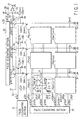
- FIG. 6 is a circuit diagram showing the construction of a solid-state imaging device according to one embodiment of this invention. Like the case of FIG. 1, in FIG. 6, a solid-state imaging device having two photodiodes arranged in each unit cell is taken as an example.
- Unit cells are arranged in a two-dimensional fashion in an imaging area on a semiconductor substrate. More precisely, the unit cells are arranged in i rows and j columns, where i and j are integers. Of these unit cells, six representive ones are illustrated in FIG. 6.
- the six unit cells P are arranged in two adjacent rows m and m+1 and three adjacent columns n-1, n and n+1; they are located at intersections (m, n-1), (m, n), (m, n+1), (m+1, n-1), (m+1, n) and (m+1, n+1).
- An address pulse line LADi, first and second readout pulse lines LR1i, LR2i and reset pulse line LRSi are arranged in the horizontal direction for each pixel row of the unit cells P(i,j).
- the unit cells P(i,j) are supplied with an address pulse ⁇ ADi, first and second readout pulses ⁇ R1i, ⁇ R2i, and reset pulse ⁇ RSi from a pulse generating section 20 used as a vertical driving circuit via the address pulse line LADi, first and second readout pulse lines LR1i, LR2i and reset pulse line LRSi.
- An output signal of a pixel row selection switching circuit 30 is supplied to the pulse generating section 20.
- the pixel row selection switching circuit 30 controls the pulse generating section 20 based on a signal LA for specifying a high-resolution mode and a signal HA for specifying a high-speed driving mode which are respectively supplied to input terminals 31 and 32. With this connection, readout pulses ⁇ R1i, ⁇ R2i of different timings in the high-resolution mode and high-speed driving mode are output from the pulse generating section 20.
- vertical signals line Sj are respectively provided in the vertical direction for columns of the unit cells P(i,j).
- Current sources Ij are respectively provided between one-side ends of the vertical signal lines Sj and the ground node.
- the other ends of the vertical signal lines Sj are respectively connected to one-side ends of the current paths of shift transistors (shift gates) SHj.
- the gates of the shift transistors SHj are commonly connected to a shift pulse line LSH.
- One-side electrodes of coupling capacitors (capacitances) CAj are respectively connected to the other ends of the current paths of the shift transistors SHj and the current paths of horizontal readout transistors (horizontal readout gates) Hj used as horizontal readout switching circuits are respectively connected between the other electrodes of the capacitors CAj and a horizontal signal line 24.
- the gates of the horizontal readout transistors Hj are respectively connected to horizontal readout pulse lines LHj.
- a capacitor which is equivalently represented by a capacitor 25 is associated with the horizontal signal line 24.
- Charge storage capacitors (capacitances) CBj are respectively connected between the other electrodes of the capacitors CAj and the ground node.
- the current paths of clamping transistors (clamping gates) CLPj for offset elimination are respectively connected between connection nodes of the capacitors CAj and CBj and the positive terminal of a clamping DC power supply 23.
- the gates of the transistors CLPj are connected to a clamp line LCLP.
- the shift transistor SHj, capacitors CAj, CBj and clamping transistor CLPj constitute a noise canceller circuit used as a signal processing circuit.
- a pulse generating section 21 supplies a shift pulse ⁇ SH to the gates of the shift transistors SHj via the shift pulse line LSH and supplies a clamp pulse ⁇ CLP to the gates of the clamping transistors CLPj via the clamp pulse line LCLP to control the operations thereof.
- a pulse generating section 22 used as a horizontal driving circuit supplies horizontal readout pulses ⁇ Hj to the gates of the respective horizontal readout transistors Hj via the horizontal readout pulse lines LHj and supplies a clear pulse ⁇ CR to the gate of a potential resetting transistor (potential resetting gate) 28 via a clear pulse line LCR.
- the potential resetting transistor 28 is used for resetting the potential of a capacitor (capacitance) 25, and one end of the current path thereof is connected to the positive terminal of a DC power supply 29 for generating a potential at the reset time and the other end of the current path thereof is connected to the horizontal signal line 24.
- the voltage value (which is indicated by Vb) of the DC power supply 29 is determined by taking the characteristic of an output buffer circuit 26 into consideration and the clear pulse ⁇ CR is supplied to the gate of the transistor 28 to set the potential of the capacitor 25 to the potential Vb before the horizontal readout pulses ⁇ Hj are supplied.
- the horizontal signal line 24 is connected to the input terminal of the output buffer circuit 26 used as an output circuit for detecting the potential of the horizontal signal line 24, subjecting the potential to impedance conversion and outputting the potential to the exterior.
- the output end of the output buffer circuit 26 is connected to an output terminal 27.
- Each unit cell P(i,j) includes photodiodes 1-1, 1-2 as photoelectric conversion/ storage sections, readout transistors (readout gates) 2-1, 2-2 as charge readout circuits, reset transistor (reset gate) 4 as a reset circuit, potential detecting transistor (potential detecting gate) 5 as a potential detecting circuit, address transistor (address gate) 6 as an address circuit and the like.
- the anodes of the photodiodes 1-1, 1-2 are grounded and the cathodes thereof are respectively connected to one-side ends of the current paths of the readout transistors 2-1, 2-2.
- the other ends of the readout transistors 2-1, 2-2 are connected to a storage node 3 (common charge detecting section) in which charges read out from the photodiodes 1-1, 1-2 are temporarily stored and the gates thereof are respectively connected to the readout pulse lines LR1i, LR2i.
- a reset transistor 4 is connected between the storage node 3 and a power supply 7 and the gate of the reset transistor 4 is connected to a corresponding one of the reset pulse lines LRSi.
- One end of the current path of the potential detecting transistor 5 is connected to a corresponding one of the vertical signal lines Sj via the output line 8 of the corresponding unit cell P(i,j) and the gate thereof is connected to the storage node 3.
- the potential detecting transistor 5 is used for detecting the charges transferred to the storage node 3 and transmits a potential corresponding to an amount of detected charges to the corresponding vertical signal line Sj via the output line 8.
- the current path of the address transistor 6 is connected between the other end of the current path of the potential detecting transistor 5 and the power supply 7 and the gate thereof is connected to a corresponding one of the address pulse lines LADi.
- the address transistor 6 is used for activating the potential readout operation of the corresponding unit cell P(i,j). In FIG. 6, in order to clarify the drawing, power supply lines are omitted.
- the timings of pulse signals supplied to the respective unit cells P(i,j) from the pulse generating section 20 are changed by supplying a signal LA for specifying the high-resolution mode or a signal HA for specifying the high-speed driving mode to the input terminal 31 or 32 so as to cause the pixel row selection switching section 30 to control the pulse generating section 20 and thus the high-resolution mode and high-speed driving mode are selectively switched.
- the high-resolution mode is set, the same operation as in the conventional case described with reference to the timing charts of FIGS. 2 and 3 is performed, and charges are individually read out from the photodiodes 1-1, 1-2 provided in each unit cell P(i,j).
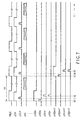
- second readout pulses ⁇ R2m, ⁇ R2m+1 are set to the high level at the same timing as first readout pulses ⁇ R1m, ⁇ R1m+1 as shown in the timing chart of FIG. 7 so as to simultaneously drive the readout transistors 2-1 and 2-2.
- light incident on the photodiodes 2-1, 2-2 is photoelectricaly converted and charges thus produced are added together in the storage node 3 and read out.
- Charges produced by photoelectrically converting light incident on the photodiodes 1-1, 1-2 are stored in the photodiodes 1-1, 1-2 until the readout transistors 2-1, 2-2 are turned ON.
- a potential determined by the gate potential of the potential detecting transistor 5 and corresponding to the charge amount of the storage node 3 is transmitted to the vertical signal line Sn-1.
- a dark current integrated value stored in the storage node 3 can be discharged by setting the reset pulse ⁇ RSm to the high level to turn ON the reset transistor 4 at the beginning of the horizontal scanning retrace interval.
- the storage node 3 can be set at the power supply voltage value (Vdd).
- a shift pulse ⁇ SH is output from the pulse generating section 21 and supplied to the gates of the shift transistors SHj to turn ON the shift transistors SHj.
- a clamp pulse ⁇ CLP is supplied from the pulse generating section 21 to the gates of the clamping transistors CLPj to turn ON the clamping transistors CLPj and perform the offset elimination process.
- the readout pulses ⁇ R1m, ⁇ R2m are set to the high level to substantially simultaneously turn ON the readout transistors 2-1 and 2-2 so that charges stored in the photodiodes 1-1, 1-2 can be transferred to and added together in the storage node 3.
- the amount of charges stored in the storage node 3 is detected by the potential detecting transistor 5 and a potential corresponding to the detected charge amount is generated and transmitted to the vertical signal line Sn-1.
- signal charges are simultaneously read out from the two photodiodes 1-1, 1-2 in each unit cell P(i,j) and supplied to the storage node 3 in the high-speed driving mode.
- the readout time for one frame is reduced by half in the same manner as in the case of FIG. 4, but in this case, the sum of the signal charges derived from the photodiodes 1-1, 1-2 is treated as one signal. Therefore, a lowering in the S/N ratio can be suppressed in comparison with the conventional technique in which the signal charge derived from one of the photodiodes is discharged via the reset transistor 4 and a lowering in the sensitivity can be suppressed since the signal charge amount is increased.
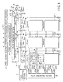
- FIG. 8 is a circuit diagram for illustrating a solid-state imaging device according to a second embodiment of this invention.
- the circuit is similar to that of FIG. 6 except that a pixel column selection circuit 40 and pixel column selection information processing circuit (decoder) 41 are provided instead of the pixel row selection switching circuit 30 and input terminals 31, 32 in the circuit of FIG. 6.
- a signal SCA for selecting a pixel column is supplied to and decoded by the pixel column selection information processing circuit 41 and the decoded signal SCA is supplied to the pixel column selection circuit 40.
- the pixel column selection circuit 40 controls the pulse generating section 22 and causes the pulse generating section 22 to output a horizontal readout pulse at different timings according to the high-resolution mode and high-speed driving mode.
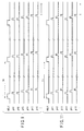
- FIG. 9 is a timing chart for illustrating the solid-state imaging device shown in FIG. 8.
- the high-resolution mode and high-speed driving mode are selectively switched.
- a horizontal readout pulse ⁇ Hj supplied to the gate of a horizontal readout transistor Hj and a horizontal readout pulse ⁇ Hj+1 supplied to the gate of an adjacent horizontal readout transistor Hj+1 are simultaneously set to the high level to simultaneously turn ON the two adjacent horizontal readout transistors Hj, Hj+1 by controlling the pulse generating section 22 by use of the pixel column selection circuit 40 and pixel column selection information processing circuit 41.
- an output signal derived by averaging signal charges read out from the two selected photodiodes is obtained in the horizontal signal line 24.
- the readout time for one frame can be reduced by half.
- the S/N ratio can be improved.
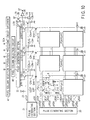
- FIG. 10 is a circuit diagram for illustrating a solid-state imaging device according to a third embodiment of this invention.
- the circuit is basically similar to that of FIG. 8 except that the control operation for controlling the pulse generating section 22 by use of a pixel column selection circuit 40' and pixel column selection information processing circuit (decoder) 41' is different, and as shown in the timing chart of FIG. 11, horizontal readout transistors arranged for every three unit cells are turned ON at the same timing. That is, signal charges are simultaneously read out from every third columns of unit cells by simultaneously setting the horizontal readout pulses ⁇ H1 and ⁇ H4, ⁇ H2 and ⁇ H5, ⁇ H3 and ⁇ H6, to the high level and the average value thereof is output.
- the readout method described in the third embodiment is preferable for a construction (RGB stripe filter) in which color filters corresponding to RGB are arranged in a stripe form.
- RGB stripe filter color filters corresponding to RGB are arranged in a stripe form.
- the other basic construction, operation and effect are the same as those described with reference to FIG. 8.
- a solid-state imaging device for averaging signals read out from a plurality of vertical signal lines and outputting the averaged value is known in the art.
- this type of solid-state imaging device an example for effecting the operation (high-resolution mode) for independently and sequentially scanning outputs of individual photodiodes arranged on the same row in the horizontal direction and outputting the same and effecting the operation (high-speed driving mode) for sequentially scanning the average of outputs of two adjacent photodiodes in the horizontal direction and outputting the same is already disclosed in Jpn. Pat. Appln. KOKAI Publication No. 10-4520.
- One of the basic ideas of this invention is that a potential signal corresponding to the average value of outputs from vertical signal lines corresponding to the selected horizontal readout transistors can be obtained on the horizontal signal line when preset timing is set to turn ON some of the horizontal readout transistors at the same time.
- Vij mQij/Cij+mVdd+V0ij
- m indicates the modulation degree of the transistor
- V0ij indicates a threshold voltage of the transistor 5 and expresses an offset voltage determined by a variation in the current source Ij.
- V (CH ⁇ Vb+NVrefCB)/(CH+NCB) +[CACB/(CA+CB) ⁇ (CH/N+CB)] ⁇ [(1/N)m ⁇ Qij/Cij]
- the fourth embodiment of this invention is explained with reference to the solid-state imaging device of FIG. 6 and the timing chart of FIG. 12.
- the fourth embodiment is suitable for AGC for controlling the shutter speed and diaphragm opening to attain adequate exposure of a video camera, electronic still camera or the like by using the average value of readout signal charges as described above.
- a pulse generating section for an electronic shutter is provided in addition to the readout pulse generating sections 20, 21, 22 as shown in FIG. 6.
- the pulse generating section for the electronic shutter outputs various pulse signals to scan unit cell rows to be selected at preset timings.
- the pulse generating section for the electronic shutter and the pulse generating section used as the vertical driving circuit are constructed by use of shit registers, for example. Specific to-be-selected rows are selected and controlled at two timings in one field period by the pulse generating section for the electronic shutter and the pulse generating section used as the vertical driving circuit.
- the electronic shutter operation for controlling the light receiving time can be equivalently attained by causing the pulse generating section for the electronic shutter to selectively control the to-be-selected row and start storage of a pixel signal before the pulse generating section used as the vertical driving circuit selectively controls the to-be-selected row and reads out a pixel signal to the vertical signal line.
- the timing chart shown in FIG. 12 illustrates a determination method of illuminance on the sensor surface for determining proper storage time (shutter speed) or diaphragm opening and is set to detect the average output of a preset representative row (for example, one row at the center of the sensor surface) before driving the sensor.
- a preset representative row for example, one row at the center of the sensor surface
- the address pulse ⁇ AD, readout pulses ⁇ R1, ⁇ R2 and reset pulse ⁇ RS generated from the pulse generating section 20 are set to the high level, and at the same time, the shift pulse ⁇ SH generated from the pulse generating section 2 and the clear pulse ⁇ CR generated from the pulse generating section 22 are set to the high level.
- the storage node 3 is connected to the Vdd power supply 7 via the reset transistor 4, and therefore, the potential is detected by the potential detecting transistor 5 and the potential of the vertical signal line (for example, Sn) is set to a high potential corresponding to the power supply voltage Vdd.
- the potential of the horizontal signal line 24 is set to a potential determined by the voltage of the DC power supply 29. Therefore, the potential of the output terminal 27 is set to a potential corresponding to the potential of the horizontal signal line 24.
- the reset transistor 4 is turned OFF, the storage node 3 is separated from the power supply 7 and the potential of the vertical signal line Sn is lowered by capacitive coupling.
- the storage time of charges into the storage node 3 is set by the interval of the readout pulse ⁇ R1 for the selected row and the potential ⁇ A of the average value (signal corresponding to the equations (16) and (17)) of sensor outputs corresponding to the storage time for one line of the selected row is output.
- the average illuminance of the sensor surface is acquired according to the potential ⁇ A and storage time setting information.
- the diaphragm opening or storage time is set according to the thus obtained average illuminance and then the normal operation is effected.
- the average illuminance of the sensor surface can be acquired by effecting the simple driving operation without performing the readout operation for all of the pixels. Further, an external memory is not necessary.
- the fourth embodiment with the first embodiment so as to use the sum of the charges read out from the two photodiodes of one unit cell as an output signal.
- the readout pulses ⁇ R1, ⁇ R2 input to each unit cell as readout pulses for the selected row can be driven substantially at the same timing.
- a solid-state imaging device capable of suppressing a lowering in the S/N ratio when the high-speed driving operation is effected can be attained.
Landscapes
- Engineering & Computer Science (AREA)
- Multimedia (AREA)
- Signal Processing (AREA)
- Transforming Light Signals Into Electric Signals (AREA)
- Solid State Image Pick-Up Elements (AREA)
Abstract
Description


Claims (12)
- A solid-state imaging device comprising an imaging area having unit cells (P(i,j)) arranged in a two-dimensional fashion on a semiconductor substrate, each of the unit cells including first and second photoelectric conversion/storage sections (1-1, 1-2) for photoelectrically converting incident light and storing charges thus generated, first and second charge readout circuits (2-1, 2-2) for transferring charges stored in the first and second photoelectric conversion/storage sections to a common charge detecting section (3), a potential detecting circuit (5) for detecting charges transferred to the charge detecting section, generating a potential corresponding to an amount of detected charges and transmitting the potential to a corresponding one of vertical signal lines (Sj), a reset circuit (4) for discharging the charges transferred to the charge detecting section, and an address circuit (6) for selectively activating the potential detecting circuit; a vertical driving circuit (20) provided in correspondence to each pixel row of said imaging area, for driving the first and second charge readout circuits, reset circuit and address circuit of each of the unit cells at preset timings; signal processing circuits (SHj, CAj, CBj, CLPj) respectively attached to the vertical signal lines (Sj) which are respectively provided for columns of the unit cells, for performing required signal processes; a horizontal driving circuit (22) for scanning outputs of said signal processing circuits in a horizontal direction at preset timings to detect the same; and an output circuit (26) for outputting output signals of said signal processing circuits detected by the scanning operation by said horizontal driving circuit; characterized in that the solid-state imaging device has a first operation mode in which the first and second charge readout circuits (2-1, 2-2) are driven at substantially the same timing by said vertical driving circuit (20), the charges stored in the first and second photoelectric conversion/storage sections (1-1, 1-2) are transferred to and added together in the charge detecting section (3), and the potential detecting circuit (5) detects the added charges, generates and transmits a potential corresponding to an amount of detected charges to the vertical signal line (Sj), and outputs the potential from said output circuit (26) via said signal processing circuits (SHj, CAj, CBj, CLPj).
- The solid-state imaging device according to claim 1, characterized by further comprising a pixel row selection switching section (30) for controlling said vertical driving circuit (20) based on a signal for specifying the first operation mode and a signal for specifying a second operation mode and
characterized in that the first and second charge readout circuits (2-1, 2-2) are driven by said vertical driving circuit (20) at substantially the same timing in the first operation mode and the first and second charge readout circuits (2-1, 2-2) are driven by said vertical driving circuit (20) at different timings in the second operation mode. - The solid-state imaging device according to claim 1, characterized in that said vertical driving circuit includes a pulse generating section (20) for outputting an address pulse (ADi), first and second readout pulses (R1i, R2i) and reset pulse (RSi).
- The solid-state imaging device according to claim 1, characterized in that each of said signal processing circuits includes a noise canceller circuit (SHj, CAj, CBj, CLPj).
- A solid-state imaging device comprising an imaging area having unit cells (P(i,j)) arranged in a two-dimensional fashion on a semiconductor substrate, each of the unit cells including a photoelectric conversion/storage section (1-1, 1-2) for photoelectrically converting incident light and storing charges thus generated, a charge readout circuit (2-1, 2-2) for transferring charges stored in the photoelectric conversion/storage section to a charge detecting section (3), a potential detecting circuit (5) for detecting charges transferred to the charge detecting section, generating a potential corresponding to an amount of detected charges and transmitting the potential to a corresponding one of vertical signal lines (Sj), a reset circuit (4) for discharging the charges transferred to the charge detecting section, and an address circuit (6) for selectively activating the potential detecting circuit; a vertical driving circuit (20) provided in correspondence to each pixel row of said imaging area, for driving the charge readout circuit, reset circuit and address circuit of each of the unit cells at preset timings; signal processing circuits (SHj, CAj, CBj, CLPj) respectively attached to the vertical signal lines which are respectively provided for columns of the unit cells, for performing required signal processes; horizontal readout switching circuits Hj) for controlling transfer of outputs of said signal processing circuits corresponding to the respective vertical signal lines (Sj) to a horizontal signal line; a horizontal driving circuit (22) for controlling said horizontal readout switching circuits at preset timings; and an output circuit for outputting output signals of said signal processing circuits which are read out to the horizontal signal line by controlling said horizontal readout switching circuits (Hj) by use of said horizontal driving circuit; characterized in that the solid-state imaging device has a first operation mode in which said horizontal driving circuit (22) sequentially turns ON said horizontal readout switching circuits (Hj) in correspondence to the vertical signal lines (Sj) to sequentially output the output signals of said signal processing circuits (SHj, CAj, CBj, CLPj) corresponding to the vertical signal lines from said output circuit (26) via the horizontal signal line and a second operation mode in which said horizontal driving circuit (22) turns ON said horizontal readout switching circuits (Hj) corresponding to plural ones of the vertical signal lines (Sj) at substantially the same time to read out the output signals of said signal processing circuits (SHj, CAj, CBj, CLPj) corresponding to the plurality of vertical signal lines to the horizontal signal line, average the output signals, and output the averaged output signal from said output circuit (26).
- The solid-state imaging device according to claim 5, characterized by further comprising a pixel column selection information processing circuit (41) supplied with a signal for selecting a pixel column, for decoding the signal for selecting a pixel column; and a pixel column selection circuit (40) supplied with a decoded output of said pixel column selection information processing circuit, for making switching between the first and second operation modes by controlling said horizontal driving circuit (22) to output horizontal output pulses at different timings in the first and second operation modes.
- The solid-state imaging device according to claim 5, characterized in that said horizontal driving circuit includes a pulse generating section (22) for outputting a horizontal readout pulse (Hj) and clear pulse ( CR).
- The solid-state imaging device according to claim 5, characterized in that said horizontal readout switching circuits (Hj) include a group of transistors which are supplied with the outputs of said signal processing circuits (SHj, CAj, CBj, CLPj) corresponding to the vertical signal lines (Sj) at one-side ends of current paths thereof and commonly connected to the horizontal signal line at the other ends of the current paths and whose gates are supplied with the output signals of said horizontal driving circuit (22), said transistors being sequentially turned ON in the first operation mode and a plurality of transistors among said group of transistors being turned ON at substantially the same time in the second operation mode.
- The solid-state imaging device according to claim 5, characterized in that each of said signal processing circuits (SHj, CAj, CBj, CLPj) includes a noise canceller circuit.
- A readout method of a solid-state imaging device which includes an imaging area having unit cells (P(i,j)) arranged in a two-dimensional fashion on a semiconductor substrate, each of the unit cells including first and second photoelectric conversion/ storage sections (1-1, 1-2) for photoelectrically converting incident light and storing charges thus generated, first and second charge readout circuits (2-1, 2-2) for transferring charges stored in the first and second photoelectric conversion/storage sections to a common charge detecting section (3), a potential detecting circuit (5) for detecting charges transferred to the charge detecting section, generating a potential corresponding to an amount of detected charges and transmitting the potential to a corresponding one of vertical signal lines (Sj), a reset circuit (4) for discharging the charges transferred to the charge detecting section, and an address circuit (6) for selectively activating the potential detecting circuit; a vertical driving circuit (20) provided in correspondence to each pixel row of the imaging area, for driving the first and second charge readout circuits, reset circuit and address circuit of each of the unit cells at preset timings; signal processing circuit (SHj, CAj, CBj, CLPj) respectively attached to the vertical signal lines (Sj) which are respectively provided for columns of the unit cells, for performing required signal processes; a horizontal driving circuit (22) for scanning outputs of the signal processing circuits in a horizontal direction at preset timing to detect the same; and an output circuit (26) for outputting output signals of the signal processing circuits detected by the scanning operation by the horizontal driving circuit, characterized by comprising the steps of driving the first and second charge readout circuits (2-1, 2-2) at substantially the same timing by use of the vertical driving circuit (20); transferring the charges stored in the first and second photoelectric conversion/storage sections (1-1, 1-2) to the charge detecting section (3) and adding the charges together; detecting the added charges by use of the potential detecting circuit (5); generating a potential corresponding to the amount of the detected charges and transmitting the potential to the vertical signal line (Sj); and outputting the potential from the output circuit (26) via the signal processing circuit (SHj, CAj, CBj, CLPj).
- A readout method of a solid-state imaging device which has first and second operation modes and includes an imaging area having unit cells (P(i,j)) arranged in a two-dimensional fashion on a semiconductor substrate, each of the unit cells including a photoelectric conversion/storage section (1-1, 1-2) for photoelectrically converting incident light and storing charges thus generated, a charge readout circuit (2-1, 2-2) for transferring charges stored in the photoelectric conversion/storage section to a charge detecting section (3), a potential detecting circuit (5) for detecting charges transferred to the charge detecting section, generating a potential corresponding to an amount of detected charges and transmitting the potential to a corresponding one of vertical signal lines (Sj), a reset circuit (4) for discharging the charges transferred to the charge detecting section, and an address circuit (6) for selectively activating the potential detecting circuit; a vertical driving circuit (20) provided in correspondence to each pixel row of the imaging area, for driving the charge readout circuit, reset circuit and address circuit of each of the unit cells at preset timings, signal processing circuits (SHj, CAj, CBj, CLPj) respectively attached to the vertical signal lines (Sj) which are respectively provided for columns of the unit cells, for performing required signal processes; horizontal readout switching circuits (Hj) for controlling transfer of outputs of the signal processing circuits corresponding to the respective vertical signal lines (Sj) to a horizontal signal line; a horizontal driving circuit (22) for controlling the horizontal readout switching circuits at preset timings; and an output circuit (26) for outputting output signals of the signal processing circuits which are read out to the horizontal signal line by controlling the horizontal readout switching circuits by use of the horizontal driving circuit; characterized in that the first operation mode comprises the steps of sequentially turning ON the horizontal readout switching circuits (Hj) corresponding to the vertical signal lines (Sj) by use of the horizontal driving circuit (22); and sequentially outputting the output signals of the signal processing circuits (SHj, CAj, CB, CLP) corresponding to the vertical signal lines (Sj) from the output circuit (26) via the horizontal signal line; and the second operation mode comprises the steps of turning ON the horizontal readout switching circuits corresponding to plural ones of the vertical signal lines (Sj) at substantially the same time; reading out the output signals of the signal processing circuits (SHj, CAj, CBj, CLPj) corresponding to the plurality of vertical signal lines (Sj) to the horizontal signal line and averaging the output signals; and outputting the averaged output signals of the signal processing circuits from the output circuit (26).
- The readout method of the solid-state imaging device according to claim 11, characterized in that the horizontal readout switching circuits (Hj) include a group of transistors whose current paths are respectively supplied at one end thereof with the outputs of the signal processing circuits (SHj, CAj, CBj, CLPj) corresponding to the vertical signal lines (Sj) and are commonly connected at the other end thereof to the horizontal signal line and whose gates are respectively supplied with the output signals of the horizontal driving circuit, said group of transistors are controlled to be sequentially turned ON in said first step and a plurality of transistors among said group of transistors are turned ON at substantially the same time in said second step.
Applications Claiming Priority (2)
| Application Number | Priority Date | Filing Date | Title |
|---|---|---|---|
| JP2000090061A JP2001285717A (en) | 2000-03-29 | 2000-03-29 | Solid-state imaging device |
| JP2000090061 | 2000-03-29 |
Publications (3)
| Publication Number | Publication Date |
|---|---|
| EP1139658A2 true EP1139658A2 (en) | 2001-10-04 |
| EP1139658A3 EP1139658A3 (en) | 2003-03-19 |
| EP1139658B1 EP1139658B1 (en) | 2005-05-11 |
Family
ID=18605721
Family Applications (1)
| Application Number | Title | Priority Date | Filing Date |
|---|---|---|---|
| EP01106500A Expired - Lifetime EP1139658B1 (en) | 2000-03-29 | 2001-03-26 | Amplification type solid-state imaging device and high-speed readout method |
Country Status (5)
| Country | Link |
|---|---|
| US (1) | US6982759B2 (en) |
| EP (1) | EP1139658B1 (en) |
| JP (1) | JP2001285717A (en) |
| KR (1) | KR100384671B1 (en) |
| DE (1) | DE60110672T2 (en) |
Cited By (5)
| Publication number | Priority date | Publication date | Assignee | Title |
|---|---|---|---|---|
| WO2018046688A1 (en) * | 2016-09-08 | 2018-03-15 | Gvbb Holdings, S.A.R.L. | System and method for dynamic pixel management of a cross pixel interconnected cmos image sensor |
| US10270997B2 (en) | 2016-09-08 | 2019-04-23 | Gvbb Holdings S.A.R.L. | Cross pixel interconnection |
| US10531034B2 (en) | 2016-09-08 | 2020-01-07 | Grass Valley Canada | Shared photodiode reset in a 5 transistor-four shared pixel |
| US10944922B2 (en) | 2016-09-08 | 2021-03-09 | Gvbb Holdings S.A.R.L | Hybrid output multiplexer for a high framerate CMOS imager |
| US11272129B2 (en) | 2016-09-08 | 2022-03-08 | Grass Valley Canada | Imager with vertical row addressing |
Families Citing this family (58)
| Publication number | Priority date | Publication date | Assignee | Title |
|---|---|---|---|---|
| US10308265B2 (en) | 2006-03-20 | 2019-06-04 | Ge Global Sourcing Llc | Vehicle control system and method |
| US10569792B2 (en) | 2006-03-20 | 2020-02-25 | General Electric Company | Vehicle control system and method |
| US9733625B2 (en) | 2006-03-20 | 2017-08-15 | General Electric Company | Trip optimization system and method for a train |
| JP4094364B2 (en) * | 2002-07-19 | 2008-06-04 | 富士フイルム株式会社 | Solid-state imaging device and photometric method thereof |
| JP4053858B2 (en) * | 2002-09-30 | 2008-02-27 | 富士フイルム株式会社 | Signal readout method for solid-state imaging device |
| KR100581296B1 (en) * | 2002-12-05 | 2006-05-17 | 주식회사 애트랩 | Image sensor for motion detection and image signal processing system using it |
| US20100225579A1 (en) * | 2002-12-05 | 2010-09-09 | Atlab Inc. | Image sensor and optical pointing system |
| US7738014B2 (en) * | 2002-12-05 | 2010-06-15 | Atlab Inc. | Image sensor and optical pointing system |
| US8924049B2 (en) * | 2003-01-06 | 2014-12-30 | General Electric Company | System and method for controlling movement of vehicles |
| DE602004021985D1 (en) * | 2003-03-25 | 2009-08-27 | Panasonic Corp | Image pickup avoiding detail loss of shady areas |
| JP4161855B2 (en) | 2003-09-10 | 2008-10-08 | ソニー株式会社 | Solid-state imaging device, drive control method, and drive control device |
| JP4288135B2 (en) * | 2003-10-27 | 2009-07-01 | 富士フイルム株式会社 | MOS type image sensor |
| JP4220406B2 (en) * | 2004-02-03 | 2009-02-04 | 富士フイルム株式会社 | Solid-state imaging device, image recording method thereof, and image reproducing method thereof |
| JP4421353B2 (en) * | 2004-04-01 | 2010-02-24 | 浜松ホトニクス株式会社 | Solid-state imaging device |
| JP4230406B2 (en) * | 2004-04-27 | 2009-02-25 | 富士通マイクロエレクトロニクス株式会社 | Solid-state imaging device |
| JP4744828B2 (en) * | 2004-08-26 | 2011-08-10 | 浜松ホトニクス株式会社 | Photodetector |
| JP5043448B2 (en) * | 2006-03-10 | 2012-10-10 | キヤノン株式会社 | Radiation imaging apparatus and radiation imaging system |
| US9689681B2 (en) | 2014-08-12 | 2017-06-27 | General Electric Company | System and method for vehicle operation |
| US9828010B2 (en) | 2006-03-20 | 2017-11-28 | General Electric Company | System, method and computer software code for determining a mission plan for a powered system using signal aspect information |
| JP2009044592A (en) * | 2007-08-10 | 2009-02-26 | Fujifilm Corp | Solid-state image sensor driving apparatus and imaging apparatus |
| JP4747154B2 (en) * | 2007-11-22 | 2011-08-17 | 富士フイルム株式会社 | Solid-state imaging device driving method, solid-state imaging device, and imaging apparatus |
| JP5129035B2 (en) * | 2008-06-17 | 2013-01-23 | オリンパス株式会社 | Solid-state imaging device |
| US8913166B2 (en) * | 2009-01-21 | 2014-12-16 | Canon Kabushiki Kaisha | Solid-state imaging apparatus |
| US9834237B2 (en) | 2012-11-21 | 2017-12-05 | General Electric Company | Route examining system and method |
| US8130304B2 (en) * | 2009-07-24 | 2012-03-06 | Aptina Imaging Corporation | Image sensors with pixel charge summing |
| US9669851B2 (en) | 2012-11-21 | 2017-06-06 | General Electric Company | Route examination system and method |
| US9682716B2 (en) | 2012-11-21 | 2017-06-20 | General Electric Company | Route examining system and method |
| US9293500B2 (en) | 2013-03-01 | 2016-03-22 | Apple Inc. | Exposure control for image sensors |
| US9276031B2 (en) | 2013-03-04 | 2016-03-01 | Apple Inc. | Photodiode with different electric potential regions for image sensors |
| US9741754B2 (en) | 2013-03-06 | 2017-08-22 | Apple Inc. | Charge transfer circuit with storage nodes in image sensors |
| US9549099B2 (en) | 2013-03-12 | 2017-01-17 | Apple Inc. | Hybrid image sensor |
| US9319611B2 (en) | 2013-03-14 | 2016-04-19 | Apple Inc. | Image sensor with flexible pixel summing |
| US9596423B1 (en) | 2013-11-21 | 2017-03-14 | Apple Inc. | Charge summing in an image sensor |
| US9596420B2 (en) | 2013-12-05 | 2017-03-14 | Apple Inc. | Image sensor having pixels with different integration periods |
| US9473706B2 (en) | 2013-12-09 | 2016-10-18 | Apple Inc. | Image sensor flicker detection |
| US10285626B1 (en) | 2014-02-14 | 2019-05-14 | Apple Inc. | Activity identification using an optical heart rate monitor |
| US9232150B2 (en) | 2014-03-12 | 2016-01-05 | Apple Inc. | System and method for estimating an ambient light condition using an image sensor |
| US9277144B2 (en) | 2014-03-12 | 2016-03-01 | Apple Inc. | System and method for estimating an ambient light condition using an image sensor and field-of-view compensation |
| US9584743B1 (en) | 2014-03-13 | 2017-02-28 | Apple Inc. | Image sensor with auto-focus and pixel cross-talk compensation |
| US9497397B1 (en) | 2014-04-08 | 2016-11-15 | Apple Inc. | Image sensor with auto-focus and color ratio cross-talk comparison |
| US9538106B2 (en) | 2014-04-25 | 2017-01-03 | Apple Inc. | Image sensor having a uniform digital power signature |
| US9686485B2 (en) | 2014-05-30 | 2017-06-20 | Apple Inc. | Pixel binning in an image sensor |
| KR102332942B1 (en) * | 2015-11-27 | 2021-12-01 | 에스케이하이닉스 주식회사 | Counting apparatus for power consumption reduction, and analog-digital converting apparatus and cmos image sensor thereof using that |
| US9912883B1 (en) | 2016-05-10 | 2018-03-06 | Apple Inc. | Image sensor with calibrated column analog-to-digital converters |
| US10658419B2 (en) | 2016-09-23 | 2020-05-19 | Apple Inc. | Stacked backside illuminated SPAD array |
| CN110235024B (en) | 2017-01-25 | 2022-10-28 | 苹果公司 | SPAD detector with modulation sensitivity |
| US10656251B1 (en) | 2017-01-25 | 2020-05-19 | Apple Inc. | Signal acquisition in a SPAD detector |
| US10962628B1 (en) | 2017-01-26 | 2021-03-30 | Apple Inc. | Spatial temporal weighting in a SPAD detector |
| US10622538B2 (en) | 2017-07-18 | 2020-04-14 | Apple Inc. | Techniques for providing a haptic output and sensing a haptic input using a piezoelectric body |
| US10440301B2 (en) | 2017-09-08 | 2019-10-08 | Apple Inc. | Image capture device, pixel, and method providing improved phase detection auto-focus performance |
| US10848693B2 (en) | 2018-07-18 | 2020-11-24 | Apple Inc. | Image flare detection using asymmetric pixels |
| US11019294B2 (en) | 2018-07-18 | 2021-05-25 | Apple Inc. | Seamless readout mode transitions in image sensors |
| US11233966B1 (en) | 2018-11-29 | 2022-01-25 | Apple Inc. | Breakdown voltage monitoring for avalanche diodes |
| US11563910B2 (en) | 2020-08-04 | 2023-01-24 | Apple Inc. | Image capture devices having phase detection auto-focus pixels |
| US12356740B2 (en) | 2020-09-25 | 2025-07-08 | Apple Inc. | Transistor integration with stacked single-photon avalanche diode (SPAD) pixel arrays |
| US11546532B1 (en) | 2021-03-16 | 2023-01-03 | Apple Inc. | Dynamic correlated double sampling for noise rejection in image sensors |
| US12192644B2 (en) | 2021-07-29 | 2025-01-07 | Apple Inc. | Pulse-width modulation pixel sensor |
| US12069384B2 (en) | 2021-09-23 | 2024-08-20 | Apple Inc. | Image capture devices having phase detection auto-focus pixels |
Family Cites Families (24)
| Publication number | Priority date | Publication date | Assignee | Title |
|---|---|---|---|---|
| JP2812990B2 (en) * | 1989-05-31 | 1998-10-22 | コニカ株式会社 | Solid-state image sensor and signal processing circuit for solid-state image sensor |
| JPH0313079A (en) * | 1989-06-09 | 1991-01-22 | Mitsubishi Electric Corp | Solid-state image pickup device |
| US5262871A (en) * | 1989-11-13 | 1993-11-16 | Rutgers, The State University | Multiple resolution image sensor |
| JP3277555B2 (en) | 1992-05-25 | 2002-04-22 | ソニー株式会社 | Amplification type solid-state imaging device |
| JPH08111517A (en) * | 1994-10-07 | 1996-04-30 | Sony Corp | Pixel signal readout method and solid-state imaging device using the same |
| JP3862298B2 (en) | 1994-12-22 | 2006-12-27 | キヤノン株式会社 | Photoelectric conversion device |
| JP3529190B2 (en) * | 1995-04-03 | 2004-05-24 | オリンパス株式会社 | Solid-state imaging device |
| WO1997007630A1 (en) * | 1995-08-11 | 1997-02-27 | Kabushiki Kaisha Toshiba | Mos image pickup device |
| JP3825503B2 (en) * | 1996-06-14 | 2006-09-27 | 浜松ホトニクス株式会社 | Solid-state imaging device |
| US6674470B1 (en) * | 1996-09-19 | 2004-01-06 | Kabushiki Kaisha Toshiba | MOS-type solid state imaging device with high sensitivity |
| JP3461265B2 (en) | 1996-09-19 | 2003-10-27 | 株式会社東芝 | Solid-state imaging device and solid-state imaging device application system |
| JPH10191184A (en) * | 1996-12-20 | 1998-07-21 | Olympus Optical Co Ltd | Solid-state imaging device |
| JPH10257397A (en) * | 1997-03-12 | 1998-09-25 | Sony Corp | Solid-state imaging device |
| US6107655A (en) * | 1997-08-15 | 2000-08-22 | Eastman Kodak Company | Active pixel image sensor with shared amplifier read-out |
| KR100487501B1 (en) * | 1997-09-25 | 2005-08-04 | 삼성전자주식회사 | Image sensor device |
| US6714239B2 (en) * | 1997-10-29 | 2004-03-30 | Eastman Kodak Company | Active pixel sensor with programmable color balance |
| JP4015242B2 (en) * | 1997-10-30 | 2007-11-28 | 浜松ホトニクス株式会社 | CCD camera |
| JP3546985B2 (en) * | 1997-12-15 | 2004-07-28 | シャープ株式会社 | Amplifying photoelectric conversion element, amplifying solid-state imaging device, and method of driving the same |
| US6801256B1 (en) * | 1998-06-02 | 2004-10-05 | Kabushiki Kaisha Toshiba | High-speed solid-state imaging device capable of suppressing image noise |
| KR100265364B1 (en) * | 1998-06-27 | 2000-09-15 | 김영환 | Cmos image sensor with wide dynamic range |
| US6507365B1 (en) * | 1998-11-30 | 2003-01-14 | Kabushiki Kaisha Toshiba | Solid-state imaging device |
| US6657665B1 (en) * | 1998-12-31 | 2003-12-02 | Eastman Kodak Company | Active Pixel Sensor with wired floating diffusions and shared amplifier |
| US6697114B1 (en) * | 1999-08-13 | 2004-02-24 | Foveon, Inc. | Triple slope pixel sensor and arry |
| JP3875461B2 (en) * | 2000-07-06 | 2007-01-31 | 株式会社東芝 | Solid-state imaging system |
-
2000
- 2000-03-29 JP JP2000090061A patent/JP2001285717A/en not_active Abandoned
-
2001
- 2001-03-26 EP EP01106500A patent/EP1139658B1/en not_active Expired - Lifetime
- 2001-03-26 US US09/816,518 patent/US6982759B2/en not_active Expired - Lifetime
- 2001-03-26 DE DE60110672T patent/DE60110672T2/en not_active Expired - Lifetime
- 2001-03-29 KR KR10-2001-0016554A patent/KR100384671B1/en not_active Expired - Fee Related
Cited By (7)
| Publication number | Priority date | Publication date | Assignee | Title |
|---|---|---|---|---|
| WO2018046688A1 (en) * | 2016-09-08 | 2018-03-15 | Gvbb Holdings, S.A.R.L. | System and method for dynamic pixel management of a cross pixel interconnected cmos image sensor |
| US10270997B2 (en) | 2016-09-08 | 2019-04-23 | Gvbb Holdings S.A.R.L. | Cross pixel interconnection |
| US10270987B2 (en) | 2016-09-08 | 2019-04-23 | Gvbb Holdings S.A.R.L. | System and methods for dynamic pixel management of a cross pixel interconnected CMOS image sensor |
| US10531034B2 (en) | 2016-09-08 | 2020-01-07 | Grass Valley Canada | Shared photodiode reset in a 5 transistor-four shared pixel |
| US10944922B2 (en) | 2016-09-08 | 2021-03-09 | Gvbb Holdings S.A.R.L | Hybrid output multiplexer for a high framerate CMOS imager |
| US11272129B2 (en) | 2016-09-08 | 2022-03-08 | Grass Valley Canada | Imager with vertical row addressing |
| US11356621B2 (en) | 2016-09-08 | 2022-06-07 | Grass Valley Canada | Hybrid output multiplexer for a high framerate CMOS imager |
Also Published As
| Publication number | Publication date |
|---|---|
| DE60110672T2 (en) | 2006-02-02 |
| EP1139658B1 (en) | 2005-05-11 |
| KR100384671B1 (en) | 2003-05-22 |
| KR20010093769A (en) | 2001-10-29 |
| DE60110672D1 (en) | 2005-06-16 |
| US6982759B2 (en) | 2006-01-03 |
| US20010026321A1 (en) | 2001-10-04 |
| JP2001285717A (en) | 2001-10-12 |
| EP1139658A3 (en) | 2003-03-19 |
Similar Documents
| Publication | Publication Date | Title |
|---|---|---|
| EP1139658B1 (en) | Amplification type solid-state imaging device and high-speed readout method | |
| US6747699B2 (en) | Solid state image pickup apparatus | |
| US5331421A (en) | Solid state image pickup apparatus | |
| US6947087B2 (en) | Solid-state imaging device with dynamic range control | |
| US6507365B1 (en) | Solid-state imaging device | |
| US8253836B2 (en) | Solid-state imaging device, imaging device and driving method of solid-state imaging device | |
| US9490291B2 (en) | Solid state imaging device and camera system | |
| US5019702A (en) | Photoelectric transducer apparatus having a plurality of transducer elements and a plurality of capacitor elements | |
| US5737016A (en) | Solid state image pickup apparatus for reducing noise | |
| US20040080645A1 (en) | Image pickup apparatus | |
| US20080204586A1 (en) | Image sensor for still or video photography | |
| US5311320A (en) | Solid state image pickup apparatus | |
| GB2130045A (en) | Line transfer imager and television camera including such an imager | |
| US8319873B2 (en) | Solid-state imaging device | |
| US7379107B2 (en) | Image sensor for still or video photography | |
| KR100426907B1 (en) | Solid-state image pickup system | |
| US5500675A (en) | Method of driving solid-state image sensing device |
Legal Events
| Date | Code | Title | Description |
|---|---|---|---|
| PUAI | Public reference made under article 153(3) epc to a published international application that has entered the european phase |
Free format text: ORIGINAL CODE: 0009012 |
|
| 17P | Request for examination filed |
Effective date: 20010326 |
|
| AK | Designated contracting states |
Kind code of ref document: A2 Designated state(s): AT BE CH CY DE DK ES FI FR GB GR IE IT LI LU MC NL PT SE TR |
|
| AX | Request for extension of the european patent |
Free format text: AL;LT;LV;MK;RO;SI |
|
| PUAL | Search report despatched |
Free format text: ORIGINAL CODE: 0009013 |
|
| AK | Designated contracting states |
Kind code of ref document: A3 Designated state(s): AT BE CH CY DE DK ES FI FR GB GR IE IT LI LU MC NL PT SE TR |
|
| AX | Request for extension of the european patent |
Extension state: AL LT LV MK RO SI |
|
| RIC1 | Information provided on ipc code assigned before grant |
Ipc: 7H 01L 27/146 B Ipc: 7H 04N 5/335 A |
|
| 17Q | First examination report despatched |
Effective date: 20030422 |
|
| AKX | Designation fees paid |
Designated state(s): DE FR GB |
|
| GRAP | Despatch of communication of intention to grant a patent |
Free format text: ORIGINAL CODE: EPIDOSNIGR1 |
|
| GRAS | Grant fee paid |
Free format text: ORIGINAL CODE: EPIDOSNIGR3 |
|
| GRAA | (expected) grant |
Free format text: ORIGINAL CODE: 0009210 |
|
| AK | Designated contracting states |
Kind code of ref document: B1 Designated state(s): DE FR GB |
|
| REG | Reference to a national code |
Ref country code: GB Ref legal event code: FG4D |
|
| REG | Reference to a national code |
Ref country code: IE Ref legal event code: FG4D |
|
| REF | Corresponds to: |
Ref document number: 60110672 Country of ref document: DE Date of ref document: 20050616 Kind code of ref document: P |
|
| PLBE | No opposition filed within time limit |
Free format text: ORIGINAL CODE: 0009261 |
|
| STAA | Information on the status of an ep patent application or granted ep patent |
Free format text: STATUS: NO OPPOSITION FILED WITHIN TIME LIMIT |
|
| 26N | No opposition filed |
Effective date: 20060214 |
|
| EN | Fr: translation not filed | ||
| PGFP | Annual fee paid to national office [announced via postgrant information from national office to epo] |
Ref country code: FR Payment date: 20070331 Year of fee payment: 7 |
|
| PG25 | Lapsed in a contracting state [announced via postgrant information from national office to epo] |
Ref country code: FR Free format text: LAPSE BECAUSE OF NON-PAYMENT OF DUE FEES Effective date: 20080330 |
|
| PGFP | Annual fee paid to national office [announced via postgrant information from national office to epo] |
Ref country code: GB Payment date: 20110323 Year of fee payment: 11 |
|
| PGFP | Annual fee paid to national office [announced via postgrant information from national office to epo] |
Ref country code: DE Payment date: 20120411 Year of fee payment: 12 |
|
| GBPC | Gb: european patent ceased through non-payment of renewal fee |
Effective date: 20120326 |
|
| PG25 | Lapsed in a contracting state [announced via postgrant information from national office to epo] |
Ref country code: GB Free format text: LAPSE BECAUSE OF NON-PAYMENT OF DUE FEES Effective date: 20120326 |
|
| REG | Reference to a national code |
Ref country code: DE Ref legal event code: R119 Ref document number: 60110672 Country of ref document: DE Effective date: 20131001 |
|
| PG25 | Lapsed in a contracting state [announced via postgrant information from national office to epo] |
Ref country code: DE Free format text: LAPSE BECAUSE OF NON-PAYMENT OF DUE FEES Effective date: 20131001 |