EP1139424A2 - Semiconductor device and method of manufacturing the same - Google Patents
Semiconductor device and method of manufacturing the same Download PDFInfo
- Publication number
- EP1139424A2 EP1139424A2 EP01302597A EP01302597A EP1139424A2 EP 1139424 A2 EP1139424 A2 EP 1139424A2 EP 01302597 A EP01302597 A EP 01302597A EP 01302597 A EP01302597 A EP 01302597A EP 1139424 A2 EP1139424 A2 EP 1139424A2
- Authority
- EP
- European Patent Office
- Prior art keywords
- semiconductor element
- chip
- semiconductor device
- board
- section
- Prior art date
- Legal status (The legal status is an assumption and is not a legal conclusion. Google has not performed a legal analysis and makes no representation as to the accuracy of the status listed.)
- Withdrawn
Links
Images







Classifications
-
- H—ELECTRICITY
- H10—SEMICONDUCTOR DEVICES; ELECTRIC SOLID-STATE DEVICES NOT OTHERWISE PROVIDED FOR
- H10W—GENERIC PACKAGES, INTERCONNECTIONS, CONNECTORS OR OTHER CONSTRUCTIONAL DETAILS OF DEVICES COVERED BY CLASS H10
- H10W42/00—Arrangements for protection of devices
- H10W42/40—Arrangements for protection of devices protecting against tampering, e.g. unauthorised inspection or reverse engineering
-
- H—ELECTRICITY
- H10—SEMICONDUCTOR DEVICES; ELECTRIC SOLID-STATE DEVICES NOT OTHERWISE PROVIDED FOR
- H10W—GENERIC PACKAGES, INTERCONNECTIONS, CONNECTORS OR OTHER CONSTRUCTIONAL DETAILS OF DEVICES COVERED BY CLASS H10
- H10W99/00—Subject matter not provided for in other groups of this subclass
-
- H—ELECTRICITY
- H10—SEMICONDUCTOR DEVICES; ELECTRIC SOLID-STATE DEVICES NOT OTHERWISE PROVIDED FOR
- H10D—INORGANIC ELECTRIC SEMICONDUCTOR DEVICES
- H10D62/00—Semiconductor bodies, or regions thereof, of devices having potential barriers
- H10D62/10—Shapes, relative sizes or dispositions of the regions of the semiconductor bodies; Shapes of the semiconductor bodies
- H10D62/117—Shapes of semiconductor bodies
-
- H—ELECTRICITY
- H10—SEMICONDUCTOR DEVICES; ELECTRIC SOLID-STATE DEVICES NOT OTHERWISE PROVIDED FOR
- H10W—GENERIC PACKAGES, INTERCONNECTIONS, CONNECTORS OR OTHER CONSTRUCTIONAL DETAILS OF DEVICES COVERED BY CLASS H10
- H10W42/00—Arrangements for protection of devices
-
- H—ELECTRICITY
- H10—SEMICONDUCTOR DEVICES; ELECTRIC SOLID-STATE DEVICES NOT OTHERWISE PROVIDED FOR
- H10W—GENERIC PACKAGES, INTERCONNECTIONS, CONNECTORS OR OTHER CONSTRUCTIONAL DETAILS OF DEVICES COVERED BY CLASS H10
- H10W70/00—Package substrates; Interposers; Redistribution layers [RDL]
- H10W70/60—Insulating or insulated package substrates; Interposers; Redistribution layers
- H10W70/67—Insulating or insulated package substrates; Interposers; Redistribution layers characterised by their insulating layers or insulating parts
- H10W70/68—Shapes or dispositions thereof
- H10W70/681—Shapes or dispositions thereof comprising holes not having chips therein, e.g. for outgassing, underfilling or bond wire passage
-
- H—ELECTRICITY
- H10—SEMICONDUCTOR DEVICES; ELECTRIC SOLID-STATE DEVICES NOT OTHERWISE PROVIDED FOR
- H10W—GENERIC PACKAGES, INTERCONNECTIONS, CONNECTORS OR OTHER CONSTRUCTIONAL DETAILS OF DEVICES COVERED BY CLASS H10
- H10W72/00—Interconnections or connectors in packages
- H10W72/071—Connecting or disconnecting
- H10W72/072—Connecting or disconnecting of bump connectors
- H10W72/07231—Techniques
- H10W72/07236—Soldering or alloying
-
- H—ELECTRICITY
- H10—SEMICONDUCTOR DEVICES; ELECTRIC SOLID-STATE DEVICES NOT OTHERWISE PROVIDED FOR
- H10W—GENERIC PACKAGES, INTERCONNECTIONS, CONNECTORS OR OTHER CONSTRUCTIONAL DETAILS OF DEVICES COVERED BY CLASS H10
- H10W72/00—Interconnections or connectors in packages
- H10W72/20—Bump connectors, e.g. solder bumps or copper pillars; Dummy bumps; Thermal bumps
- H10W72/251—Materials
- H10W72/252—Materials comprising solid metals or solid metalloids, e.g. PbSn, Ag or Cu
-
- H—ELECTRICITY
- H10—SEMICONDUCTOR DEVICES; ELECTRIC SOLID-STATE DEVICES NOT OTHERWISE PROVIDED FOR
- H10W—GENERIC PACKAGES, INTERCONNECTIONS, CONNECTORS OR OTHER CONSTRUCTIONAL DETAILS OF DEVICES COVERED BY CLASS H10
- H10W72/00—Interconnections or connectors in packages
- H10W72/50—Bond wires
- H10W72/551—Materials of bond wires
- H10W72/552—Materials of bond wires comprising metals or metalloids, e.g. silver
- H10W72/5522—Materials of bond wires comprising metals or metalloids, e.g. silver comprising gold [Au]
-
- H—ELECTRICITY
- H10—SEMICONDUCTOR DEVICES; ELECTRIC SOLID-STATE DEVICES NOT OTHERWISE PROVIDED FOR
- H10W—GENERIC PACKAGES, INTERCONNECTIONS, CONNECTORS OR OTHER CONSTRUCTIONAL DETAILS OF DEVICES COVERED BY CLASS H10
- H10W72/00—Interconnections or connectors in packages
- H10W72/851—Dispositions of multiple connectors or interconnections
- H10W72/874—On different surfaces
- H10W72/884—Die-attach connectors and bond wires
-
- H—ELECTRICITY
- H10—SEMICONDUCTOR DEVICES; ELECTRIC SOLID-STATE DEVICES NOT OTHERWISE PROVIDED FOR
- H10W—GENERIC PACKAGES, INTERCONNECTIONS, CONNECTORS OR OTHER CONSTRUCTIONAL DETAILS OF DEVICES COVERED BY CLASS H10
- H10W74/00—Encapsulations, e.g. protective coatings
-
- H—ELECTRICITY
- H10—SEMICONDUCTOR DEVICES; ELECTRIC SOLID-STATE DEVICES NOT OTHERWISE PROVIDED FOR
- H10W—GENERIC PACKAGES, INTERCONNECTIONS, CONNECTORS OR OTHER CONSTRUCTIONAL DETAILS OF DEVICES COVERED BY CLASS H10
- H10W74/00—Encapsulations, e.g. protective coatings
- H10W74/10—Encapsulations, e.g. protective coatings characterised by their shape or disposition
-
- H—ELECTRICITY
- H10—SEMICONDUCTOR DEVICES; ELECTRIC SOLID-STATE DEVICES NOT OTHERWISE PROVIDED FOR
- H10W—GENERIC PACKAGES, INTERCONNECTIONS, CONNECTORS OR OTHER CONSTRUCTIONAL DETAILS OF DEVICES COVERED BY CLASS H10
- H10W90/00—Package configurations
- H10W90/701—Package configurations characterised by the relative positions of pads or connectors relative to package parts
- H10W90/731—Package configurations characterised by the relative positions of pads or connectors relative to package parts of die-attach connectors
- H10W90/736—Package configurations characterised by the relative positions of pads or connectors relative to package parts of die-attach connectors between a chip and a stacked lead frame, conducting package substrate or heat sink
-
- H—ELECTRICITY
- H10—SEMICONDUCTOR DEVICES; ELECTRIC SOLID-STATE DEVICES NOT OTHERWISE PROVIDED FOR
- H10W—GENERIC PACKAGES, INTERCONNECTIONS, CONNECTORS OR OTHER CONSTRUCTIONAL DETAILS OF DEVICES COVERED BY CLASS H10
- H10W90/00—Package configurations
- H10W90/701—Package configurations characterised by the relative positions of pads or connectors relative to package parts
- H10W90/751—Package configurations characterised by the relative positions of pads or connectors relative to package parts of bond wires
- H10W90/756—Package configurations characterised by the relative positions of pads or connectors relative to package parts of bond wires between a chip and a stacked lead frame, conducting package substrate or heat sink
Definitions
- the present invention relates to a semiconductor device in which a semiconductor element is secured to a board and a method of manufacturing the same.
- chips semiconductor element chips
- IC integrated circuit
- LSI large-scale integration
- the chip when applied in a semiconductor device, is typically secured to a board and then sealed in a plastic package or the like, so as to provide protection to the chip from its external environment and allow easy handling of the chip during use.
- An example is taken here to describe an arrangement of a packaged semiconductor device having a chip with a transistor-integrated circuit (integrated circuit).
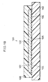
- FIG 19 is an explanatory drawing showing a conventional arrangement of a packaged semiconductor device 101.
- the semiconductor device 101 is of a flipped-chip mounting type wherein the chip 102 is positioned so that its front faces the board 103.
- a package 108 made of epoxy resin is provided to cover the back of the chip 102, thereby sealing the chip 102.
- the chip 102 is secured to the board 103 interposed by glue (anisotropic conducting glue) 105.
- the board 103 is made of glass epoxy prepared by immersing epoxy resin in glass fiber.
- the pad section 107 has a bump 104 to establish contact to a wire section 106 made of copper film on the board 103.
- the wire section 106 with output wiring for external connection is provided on the board 103 at a position that matches the position of the pad section 107 on the chip 102.
- a bump 104 is fabricated of gold on the pad section 107 of the chip 102, followed by application of glue 105 onto the board 103.
- the board 103 and chip 102 are stacked so that the wire section 106 matches the bump 104 (pad section 107) in position, thereby mounting the chip 102 on the board 103.
- the chip 102 and board 103 are compressed and secured to each other, while heating at about 200 °C.
- the glue 105 solidifies due to the heating, securing the chip 102 onto the board 103.
- the chip 102 is sealed by epoxy resin to form the package 108.
- the chip 102 has a thickness of 200 ⁇ m or more. Besides, normally, the chip 102 is secured level (flat) onto the board 103 to retain its electrical properties.
- Tokukaihei No. 11-238750 discloses a method of manufacturing a highly reliable semiconductor device of a flipped-chip mounting type by removing residual scum from a vicinity of the pad section on the chip and improving the adherence between the pad section (metal) and the bump (metal).
- Tokukaisho No. 64-15957 discloses a method of seal an NMOS type (N-type metal oxide semiconductor) element chip in a semiconductor package with a gas and liquid, whereby a mechanical pressure (stress) is applied to the chip using a gas and liquid so as to increase current flow for improved performance of the NMOS element.
- NMOS type N-type metal oxide semiconductor
- Japanese Laid-Open Patent Application No. 5-93659/1993 discloses a distortion sensor which works by means of a stress being applied to various kinds of resistor elements, which is a technology not directly related to semiconductor elements, but rather to Tokukaisho No. 64-15957.
- the distortion sensor takes advantage of a glass layer which changes its electric resistance when distorted.
- the semiconductor device 101 of a flipped-chip mounting type of Figure 19 has a structure that does not readily allow observation of the integrated circuit provided on the front of the chip 102.
- the board 103 is secured on the front of the chip 102 interposed by the glue 105. Therefore, unsealing the epoxy resin package 108 covering the back of the chip 102 permits only a look at the back of the chip 102, allowing no observation or analysis of the structure of the integrated circuit.
- the epoxy resin forming the board 103, the anisotropic conducting glue 105, etc. are removable using an etchant containing fuming nitric acid or sulfuric acid, for example. Therefore, the board 103 and glue 105 can be peeled off (removed) by the use of the etchant, separating the chip 102 from all the other parts.
- the chip 102, once separated, is prone to any kind of analysis; the integrated circuit on the front can be observable, and its electrical properties are measurable by directly contacting probes.
- the chip 102 secured level onto the board 103 in the package 108 i.e., packaged, has a thickness of 200 ⁇ m or more. Therefore, the chip 102 continues to be level even after it is separated from the all the other parts for analysis; the integrated circuit on the chip 102 operates normally exhibiting the same electrical properties as when it is packaged.
- the conventional semiconductor device 101 when the epoxy resin is peeled to separate the chip 102 from all the other parts, is highly prone to analysis on its integrated circuit and other parts due to its arrangement and package method. This gives a rise to a problem that secrets cannot be well concealed.
- Tokukaihei 11-238750 and Tokukaisho 64-15957 mentioned above disclose technologies to improve the performance of the chip, but completely fails to pay attention to methods prohibiting the analysis of the chip (integrated circuit). These technologies still allow separation of the chip from all the other parts for analysis of the integrated circuit or other members.
- Tokukaihei 5-93659 above relating to a distortion sensor, belongs basically to a different field of technology from the present invention and neither discloses nor suggests the protection of the chip from analysis.
- the present invention has an object to offer a semiconductor device which can completely prevent analysis of the integrated circuit of the semiconductor element secured to the board, as well as a method of manufacturing such a semiconductor device, i.e., to offer a semiconductor device which ensures protection of secrets about the semiconductor element, as well as a method of manufacturing such a semiconductor device.
- a semiconductor device in accordance with the present invention includes a semiconductor element, with an integrated circuit, secured to a board, is such that the semiconductor element is secured level and specified to operate normally only when the semiconductor element is level.
- the semiconductor element is specified to operate normally only when it is level. Therefore, if the semiconductor element is no longer capable of sustaining its level shape as a result of, for example, detachment of the semiconductor element from the board, the semiconductor element does not operate normally due to a resultant change and the like in its electrical properties. This ensures that any analysis is prohibited from being conducted on the integrated circuit on the semiconductor element. Thus, secrets can be concealed safely about the semiconductor element.
- a method of manufacturing a semiconductor device in accordance with the present invention includes, after securing a semiconductor element with an integrated circuit to a board so as to be level, the step of processing at least a part of a back of the semiconductor element to develop such stress that when the semiconductor element is detached from the board, at least a part thereof deforms.
- the semiconductor element is given such stress that when the semiconductor element is detached from the board, at least a part thereof deforms. Therefore, if the semiconductor element is detached from the board and can no longer sustain its level shape, the semiconductor element does not operate normally due to a resultant change and the like in its electrical properties. This ensures that any analysis is prohibited from being conducted on the integrated circuit on the semiconductor element. Thus, a semiconductor device can be manufactured in which secrets can be concealed safely about the semiconductor element.
- Figure 1(a) is a cross-sectional view schematically showing an arrangement of a semiconductor device of a first embodiment in accordance with the present invention.
- Figure 1(b) is a cross-sectional view showing the semiconductor device of Figure 1 (a) which has deformed due to removal of a semiconductor element chip from it.
- Figure 2 is a plan view schematically showing an arrangement of the semiconductor element chip of Figure 1(b).
- Figure 3 is a circuit diagram showing, as an example, an arrangement of a distortion sensor provided in a sensor section, a transistor provided in a transistor section, and an LSI circuit provided in a LSI circuit section of a semiconductor element chip of Figure 1 (b).
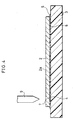
- Figure 4 in reference to an example of a manufacturing process of the semiconductor device of Figure 1(a), is a cross-sectional view showing the semiconductor element chip being secured to a board.
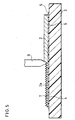
- Figure 5 in reference to an example of a manufacturing process of the semiconductor device of Figure 1(a), is a cross-sectional view showing the semiconductor element chip being processed on its back.
- Figure 6 in reference to an example of a manufacturing process of the semiconductor device of Figure 1(a), is a cross-sectional view showing the semiconductor element chip having been processed on its back.
- Figure 7 in reference to an example of a manufacturing process of the semiconductor device of Figure 1(a), is a cross-sectional view showing the semiconductor element chip having been packaged.
- Figure 8(a) is a cross-sectional view schematically showing an arrangement of a semiconductor device of a second embodiment in accordance with the present invention.
- Figure 8(b) is a cross-sectional view showing the semiconductor device of Figure 8(a) which has deformed due to removal of a semiconductor element chip from it.
- Figure 9(a) is an explanatory drawing showing a preprocessing arrangement of the semiconductor element chip of Figure 8(b).
- Figure 9(b) is a cross-sectional view showing the semiconductor element chip of Figure 8(b) which has distorted.
- Figure 10(a) is an explanatory drawing schematically showing an arrangement of a semiconductor device of a third embodiment in accordance with the present invention.
- Figure 10(b) is a cross-sectional view showing the semiconductor device of Figure 10(a) which has deformed due to removal of a semiconductor element chip from it.
- Figure 11 is a plan view schematically showing an arrangement of a lead frame in the semiconductor device of Figure 10(a).
- Figure 12 in reference to an example of a manufacturing process of the semiconductor device of Figure 10(a), is a cross-sectional view showing the semiconductor element chip having been secured to a die pad.
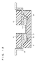
- Figure 13 in reference to an example of a manufacturing process of the semiconductor device of Figure 10(a), is a cross-sectional view showing the semiconductor element chip having been processed on its back.
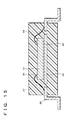
- Figure 14 in reference to an example of a manufacturing process of the semiconductor device of Figure 10(a), is a cross-sectional view showing the semiconductor element chip having been packaged.
- Figure 15 is a cross-sectional view schematically showing an arrangement of a conventional semiconductor device of a wire bonding type.
- Figure 16 is a plan view schematically showing an arrangement of a lead frame of the semiconductor device of Figure 15.
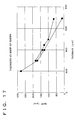
- Figure 17 is a graph showing measurements of relationships between the thickness and warp (degrees of warp) of wafers (made of chip base material) which have been thinned down from their original thickness of 725 ⁇ m by polishing.
- Figure 18 is a graph showing measurements of relationships between amounts of etching and warp of wafers whose polished surfaces have been wet etched.
- Figure 19 is a cross-sectional view schematically showing an arrangement of a conventional semiconductor device of a flipped-chip mounting type.
- a semiconductor device in accordance with the present invention (hereinafter, "the present semiconductor device") has a semiconductor element with an integrated circuit.
- the semiconductor element is secured level onto a board in, for example, a package.
- the semiconductor element is specified to operate normally only when it is level. Conversely, the semiconductor element is specified to, when it becomes no longer capable of continuing to be level, cause a change in electrical or other properties of its transistor and integrated circuit and fail to operate normally.
- the semiconductor element is receiving a stress (static stress) as a result of processing carried out on at least a part of its back and, when detached from the board in the present semiconductor device, becomes no longer capable of continuing to be level and deforms (e.g., warps) at least partially due to the stress.
- a stress static stress
- the present semiconductor device is specified in this manner, when the semiconductor element is detached from the board, the semiconductor element deforms and changes its electrical and other properties, thereby being prevented from operating normally.
- the semiconductor element, when detached, can be thus protected from property and circuit analysis.
- the present semiconductor device must be mounted to an external circuit when used.
- the present invention has an object to exploit, for various purposes, such a phenomenon that transistors, ICs (integrated circuits), and LSI (large-scale integration) circuits change their electrical properties when deformed; one of the purposes is to provide protection to the semiconductor element from analysis.
- the sensors and mounting methods which will be described in the following embodiments constitute mere examples.
- the semiconductor element being detached from the board refers to the condition in which at least a part of the semiconductor element has peeled off the board.
- a semiconductor device 1 of the present embodiment is packaged, i.e., includes a semiconductor element chip (semiconductor element; hereinafter, “chip”) 2 which is sealed in a package 8.
- chip semiconductor element chip
- the semiconductor device 1 is of a flipped-chip mounting type whereby the chip 2 is positioned so that its front faces a board 3.
- the package 8 made of epoxy resin or other material is provided in a manner to cover the chip 2 on its back, thereby sealing the chip 2.
- the board 3 formed from a glass epoxy board, has a wire section 6 made from copper foil on its side which contacts to the chip 2.
- the board 3 is fabricated by, for example, immersing epoxy resin in glass fiber.
- the chip 2 is a silicon-made semiconductor element chip and is secured onto the board 3 by a glue (anisotropic conducting glue) 5.
- the pad section 7 has a bump 4 to establish contact to a wire section 6 on the board 3.
- the back 2a of the chip 2 is subjected to rough surface processing to apply a stress to the chip 2 to deform the chip 2. Due to the processing of the back 2a, the chip 2 warps due to stress when removed from the package 8 (when detached from the board 3) as shown in Figure 1 (b) .
- a typical conventional semiconductor element has a thickness of 200 ⁇ m or more.
- the chip 2 in the semiconductor device 1 has a thickness of 50 ⁇ m or less, preferably 30 ⁇ m to 50 ⁇ m, because of the rough surface processing.
- the chip 2 is therefore thinner entirely than conventional semiconductor elements and more prone to deformation caused by the stress applied to the processed back 2a when detached from the board 3.
- FIG. 2 is an explanatory drawing showing an arrangement of the electronic circuit section.
- the electronic circuit section includes a transistor section 21, a sensor section 22 and an LSI circuit section 23.
- the transistor section 21 is a part where transistors (of an NMOS type (N-type metal oxide semiconductor)) are provided at high density.
- the sensor section 22 is a part where a detector section (detector means; will be detailed later) is provided to detect electrical properties of the transistors.
- the LSI circuit section 23 is a part where circuitry including an IC (integrated circuit) or LSI (large-scale integration) circuit is provided.
- the transistor in the transistor section 21 is specified to exhibit electrical properties according to the shape of the transistor section 21. In other words, the transistor possesses different electrical properties when the transistor section 21 is level (normal period) and when the transistor section 21 is deformed (deformed period).
- the transistor section 21 provided on the front of the chip 2 warps accordingly.
- the semiconductor device 1 is therefore specified so that when the chip 2 is detached from the board 3, the transistor in the transistor section 21 changes its electrical property.
- a stress (external force) was applied to the transistor section 21, for example, so that it warped convexly in a direction perpendicular to current flow through the transistor and normal to the front of the chip 2, and as a result, the front of the transistor section 21 actually warped due to the stress, forming a warped surface having a radius (r) of 10 mm.
- the transistor when activated, showed a 10 % increase in its channel current.
- the transistor is specified to change its electrical properties according to the shape of the transistor section 21.
- the detector section in the sensor section 22 is for detecting an electrical properties of the transistor in the transistor section 21 and controlling the LSI circuit provided in the LSI circuit section 23 according to results of the detection.
- the detector section is specified to activate the LSI circuit if it detects an electrical property exhibited by the transistor at normal period (exhibited by the transistor provided in a level part of the transistor section 21) and to deactivates the LSI circuit if it detects an electrical property exhibited by the transistor at deformed period.
- the semiconductor device 1 is specified so that the detector section detects a change in electrical properties (current, voltage, etc.) of the transistor caused by the warp of the chip 2 (transistor section 21) to utilize the results in the control of the operation of the LSI circuit.
- the detector section may OP-amplifier or another analog circuit be used for example.
- the OP-amplifier is for detecting a change in electrical properties of the transistor which occurs when the level transistor section 21 deforms.
- the electronic circuit section includes a transistor 24, a distortion sensor 25, and an LSI circuit 26.
- the distortion sensor 25 is an OP-amplifier with a resistor R and a comparator Cp, acting as the aforementioned detector section. As shown in Figure 3, in the distortion sensor 25, the resistor R is connected at one of its ends to the transistor 24 in the transistor section 21 (see Figure 2) and grounded at the other end.
- the comparator Cp has two input terminals and an output terminal. One of the input terminals is connected to a wire connecting the resistor R to the transistor 24. A predetermined voltage V 2 is applied in advance to the other input terminal. The output terminal is connected to the LSI circuit 26 in the LSI circuit section 23 (see Figure 2).
- the predetermined voltage V 2 is equal to or exceeds the characteristic voltage V 1 of the transistor 24 at normal period and is specified lower than the characteristic voltage V 1 of the transistor 24 at deformed period.
- the characteristic voltage V 1 refers to a voltage the transistor 24 generates when it receives a drive voltage. As the transistor 24 receives a drive voltage, it outputs a characteristic current I d which changes in value according to the shape of the transistor section 21. The value of the characteristic voltage V 1 is determined by the characteristic current I d and the resistor R connected to the transistor 24.
- the characteristic current I d of the transistor 24 increases in value as the transistor section 21 warps, which means that the characteristic voltage V 1 increases as the transistor section 21 warps.
- the comparator Cp compares the characteristic voltage V 1 with the predetermined voltage V 2 to determine which voltage is higher. According to its specifications, the comparator Cp outputs low signal (operation signal) from its output terminal to the LSI circuit 26 if the characteristic voltage V 1 is either lower than or equal to the predetermined voltage V 2 , and conversely, outputs high signal to the LSI circuit 26 if the characteristic voltage V 1 is higher than the predetermined voltage V 2 .
- the LSI circuit 26 has an operation prohibition circuit 27 for controlling the operation of the LSI circuit 26 itself according to an output signal of the distortion sensor 25 (comparator Cp).
- the operation prohibition circuit 27 allows the LSI circuit 26 to operate when it receives low signal from the distortion sensor 25. Meanwhile, the operation prohibition circuit 27 is specified to prohibit the operation of the LSI circuit 26 when it receives high signal or no signal at all from the distortion sensor 25. To put it differently, according to specifications, the LSI circuit 26 is allowed to operate only when it receives low signal from the distortion sensor 25.
- the transistor 24 exhibits normal electrical properties. Therefore, the predetermined voltage V 2 is equal to or exceeds the characteristic voltage V 1 (V 1 ⁇ V 2 ), causing the comparator Cp in the distortion sensor 25 to output low signal to the LSI circuit 26.
- the LSI circuit 26 hence operates normally.
- the electrical properties of the transistor 24 thereby change, and the transistor 24 outputs a characteristic current I d at an increased value. Consequently, the characteristic voltage V 1 becomes greater than the predetermined voltage V 2 (V 1 > V 2 ), and the comparator Cp in the distortion sensor 25 outputs high signal to the LSI circuit 26. Receiving the high signal, the operation prohibition circuit 27 causes the LSI circuit 26 to stop operating.
- the chip 2 is secured level onto the board 3 (with the chip being flipped). Further, the chip 2 is specified to, when detached from the board 3, deform due to the stress which develops as a result of the rough surface processing carried out on the back 2a.
- the chip 2 specified to operate normally when it is level and to fail to operate normally when it has deformed.
- the operation prohibition circuit 27 stops the LSI circuit 26 from operating.
- the LSI circuit 26 is specified to be prohibited by the operation prohibition circuit 27 from operating when it receives no signal. Therefore, the LSI circuit 26 is not operable alone (when detached from the LSI circuit section 23); in these conditions, no analysis of the circuit is ever possible by means of probing.
- a chip 2 having a thickness of 200 ⁇ m or more is prepared, including a pad section 7.
- a wire section 6 with output wiring for external connection is then provided on the board 3 at a position that matches the position of the pad section 7 of the chip 2. This is followed by fabrication of a bump 4 of gold on the pad section 7 of the chip 2.
- glue anisotropic conducting glue
- the board 3 and chip 2 are stacked so that the wire section 6 matches the bump 4 (pad section 7) in position, thereby mounting the chip 2 on the board 3.
- the chip 2 and board 3 are compressed and secured to each other, while heating at about 200 °C.
- the glue 5 solidifies due to the heating, securing the chip 2 onto the board 3.
- the chip 2 is mounted in a flipped posture to be level on the board 3.
- the board 3 on which the chip 2 is secured is loaded at a predetermined position in a dicing machine.
- the back 2a of the chip 2 is scraped (subjected to rough surface processing) entirely using a dicing blade 9 provided in the dicing machine as shown in Figure 5 and Figure 6.
- the scraping is carried out to reduce the thickness of the chip 2 to 50 ⁇ m or less, preferably to a range of 30 ⁇ m to 50 ⁇ m.
- the scraping of the back 2a by means of the dicing blade 9 is preferably carried out in a specified direction (for example, in a direction normal to the paper showing Figure 5).
- the back 2a of the chip 2 is shaped by the scraping so that the chip 2 readily deforms due to stress.
- the scrape processing carried out on the entirety of the back 2a renders the chip 2 entirely thinner, enabling predetermined stress to be applied to the chip 2 entirely.
- the chip 2 is sealed by epoxy resin using a predetermined mold to form a package 8.
- the manufacture of the semiconductor device 1 is hence completed.
- the chip 2 has its back 2a subjected to rough surface processing and therefore, has such a structure that once it is detached from the board 3 and deforms due to stress, it does not easily return to the level shape.
- the structure thereby never allows the chip 2 to completely return to the level shape even by, for example, vacuum adsorption on a level base. To put it differently, the chip 2, once deformed, by no means completely returns to the level shape. Nor can any analysis be conducted on the LSI 26 and other circuits, once the chip 2 is deformed, as described earlier.
- the chip 2 is scraped after being mounted in a flipped posture. Therefore, the chip 2 can retain its level shape inside the semiconductor device 1 even when it is thinned down and receives stress.
- the scrape processing by means of the dicing blade 9 produces no adverse effects on devices, such as the transistor 24 and LSI circuit 26 in the chip 2, which we confirmed through experiments and other methods.
- the scraping by means of the dicing blade 9 is preferably carried out so as to render the steps formed by the dicing (groove pitches formed by the scraping) as short as possible. Short steps would enable a stress to be applied to the chip 2 easily.
- the chip 2 may be thinned down entirely to some extent (for example, about 50 ⁇ m) by a typical scrape or other method, as required.
- the scraping of the back 2a of the chip 2 using the dicing blade 9 is carried out in a specified direction (for example, in a direction normal to the paper showing Figure 5); however, the scraping may be carried out in whichever direction that results in easy deformation of the chip 2 due to stress or may be carried out in two or more different directions.
- the dicing blade 9 is used in the rough surface processing of the entire back 2a of the chip 2; however, there are no particular limitations as to which part(s) of the chip 2 is(are) to be thinned down. Only the transistor section 21 may be thinned down, for example.
- the chip 2 is specified to detect electrical properties of the transistor 24 using the distortion sensor 25, as described earlier. Therefore, the chip 2 is preferably thinned down in such a manner that at least the transistor section 21 deforms due to stress.
- the present embodiment only refers to a case where the back 2a of the chip 2 is entirely scraped by dicing; however, the back 2a of the chip 2 may be scraped by a method other than dicing. Examples include physical scraping by means of sand blast or sandpaper and treatment by means of laser beam projection.
- the chip 2 is thinned down to some extent (for example, about 50 ⁇ m) by a typical scrape or other method.
- the board 3 on which the chip 2 is secured is loaded in a predetermined place in a laser marker device (laser beam projection device).
- the laser beam is preferably a converging laser beam which is a focused energy beam.
- a converging laser beam can be generated by means of, for example, a laser light source using YAG (yttrium aluminum garnet) as a solid laser medium.
- the back 2a of the chip 2 is treated by projection of a laser beam with, for example, the second harmonic wavelength of 532 nm. As a result of the treatment, numerous minute dents or irregularities are formed on the back 2a, enabling a predetermined stress to be applied to the chip 2.
- the laser beam with the above specified wavelength produces no adverse effects to devices, such as the transistor 24 and LSI circuit 26 of the chip 2, which we confirmed through experiments and other methods.
- the chip 2 is thinned down to some extent similarly to the foregoing case.
- the board 3 on which the chip 2 is secured is loaded in a predetermined place in a sand blast processing device, and the back 2a of the chip 2 is scraped so that the chip 2 has a thickness of, for example, 50 ⁇ m or less, preferably in a range of 30 ⁇ m to 50 ⁇ m.
- sand blast particles for example, #1000 (about 15 ⁇ m) are preferably used as sand blast particles (grind particles).
- the calcium carbonate particles produce no adverse effects to devices, such as the transistor 24 and LSI circuit 26 of the chip 2, which we confirmed through experiments and other methods.
- the chip 2 is thinned down to some extent similarly to the foregoing cases.
- the back 2a of the chip 2 is scraped using sandpaper so that the chip 2 has a thickness of, for example, 50 ⁇ m or less, preferably in a range of 30 ⁇ m to 50 ⁇ m.
- a thickness of, for example, 50 ⁇ m or less preferably in a range of 30 ⁇ m to 50 ⁇ m.
- the scraping by means of sandpaper is carried out manually and requires good attention. However, it is the easiest processing method.
- FIG 8(a) is an explanatory drawing showing an arrangement of a semiconductor device 11 of the present embodiment. As shown in this Figure, the semiconductor device 11 is different from the semiconductor device 1 in that the chip 2 is replaced with a chip 12.
- the chip 2 in the semiconductor device 1 has its back 2a subjected to rough surface processing.
- the chip 12 in the semiconductor device 30 is has a part of its back 12a subjected to the rough surface processing.
- the chip 12 is thinned down in the transistor section 21 (for example, to 50 ⁇ m or less) and remains at the same thickness in the sensor section 22 and LSI circuit section 23 (for example, 200 ⁇ m or more) .
- the chip 12 receives stress only in the transistor section 21 and deforms only in the transistor section 21 due to stress when detached from the board 3.
- the chip 12 only a part of the back 12a (transistor section 21) is subjected to rough surface processing, resulting in non-uniform thickness.
- the chip 12 has such a structure that once it is detached from the board 3 and deforms due to stress, it returns to the level shape only with great difficulties.
- the structure thereby never allows the chip 12 to completely return to the level shape even by, for example, vacuum adsorption on a level base. To put it differently, the chip 12, once deformed, by no means completely returns to the level shape. Nor can any analysis be conducted on the LSI 26 and other circuits, once the chip 12 is deformed, as described earlier.
- the processing may be carried out by means of, for example, scraping by dicing, or sand blast, sandpaper or treatment by laser beam projection.
- the chip 12 only needs to, when detached from the board 3, at least partially deform due to stress or preferably is such that the transistor section 21 at least partially deforms convexly or concavely.
- the package 8 may be provided only when required.
- the semiconductor device 1, 11 may not be a packaged type.
- the semiconductor device 1, 11 may not be of a flipped-chip mounting type.
- the resultant chip 2 should receive a predetermined stress so that is deforms sufficiently when detached from the board 3; and the functions of the transistor, LSI circuit, and other components on the chip 2 should not be adversely affected when the chip 2 is level. Accordingly, there are no particular limitations on the thickness of the chip 2.
- the chip preferably has a thickness of 50 ⁇ m or less and more preferably in a range of 30 ⁇ m to 50 ⁇ m.
- the chip 2 can avoid adversely affecting the functions of the transistor, LSI circuit, and other components when it is level, as well as can deform (e.g., warp) surely as desired when detached from the board 3.
- the sensor section 22 in the chip 2 is preferably interposed at least between the transistor section 21 and the LSI circuit section 23. This is because, as described earlier, the detector section is provided in the sensor section 22 so as to electrically connect the transistor to the LSI circuit.
- the sensor section 22 is not necessarily positioned between the transistor section 21 and the LSI circuit section 23, and may be positioned anywhere as long as it can electrically connect the transistor section 21 to the LSI circuit section 23. Accordingly, there is no particular limitations on the relative positions of the transistor section 21, sensor section 22, and LSI circuit section 23.
- the LSI circuit 26 shown in Figure 3 includes an operation prohibition circuit 27 which allows the LSI circuit 26 to operate only when it receives low signal from the distortion sensor 25. Accordingly, the operation prohibition circuit 27 has a function of prohibiting the LSI circuit 26 from operating when the LSI circuit 26 alone is subjected to probing for circuit analysis.
- the operation prohibition circuit 27 only needs to be arranged to have the foregoing function and is not limited in any particular manner.
- the operation prohibition circuit 27 can be assembled from a resistor, for example.
- the operation prohibition circuit 27 may be arranged so that the power source and grounding of the distortion sensor 25 are provided at a common pad with the LSI circuit 26.
- the distortion sensor 25 is not limited only to the arrangement shown in Figure 3.
- the distortion sensor 25 only needs to be arranged to be capable of detecting changes in value of the characteristic current I d of the transistor 24 caused by the deformation of the level transistor section 21.
- an arrangement may be employed which, upon detection of a characteristic current of a predetermined value (or in a predetermined range), supplies such a signal (operation signal) to the LSI circuit that causes the LSI circuit to operate normally.
- this distortion sensor Upon detection of a characteristic current of a value not equal to the predetermined value (or out of the predetermined range) or failure to detect the characteristic current, this distortion sensor preferably supplies such a signal (operation prohibit signal) to the LSI circuit that stops (prohibits) the operation of the LSI circuit.
- Another preferred arrangement is to stop the supply of the operation signal.
- a distortion sensor capable of detecting this change may be used as detector means.
- the distortion sensor is preferably arranged to detect a change in an electrical property occurring in that part and supplies a signal to the LSI circuit to prohibit the LSI circuit from operating.
- the transistor section is not the only part which deforms due to stress (in which an electrical property changes) in the chip.
- the distortion sensor may be positioned somewhere other than in the sensor section.
- FIG 10(a) is an explanatory drawing showing an arrangement of a semiconductor device 30 of the present embodiment.
- the semiconductor device 30 is of a packaged type including a silicon semiconductor element chip (semiconductor element; hereinafter, simply “chip”) 31 sealed inside an epoxy resin package 37.
- chip semiconductor element
- the chip 31 is secured onto a die pad (board) 32 interposed by a silver paste 33.
- the semiconductor device 30 On the front of the chip 31 are there provided an electronic circuit section and a pad section 35 as will be described later in detail.
- the pad section 35 is electrically connected to a lead wire 36 via a gold wire 34.
- the semiconductor device 30 has a structure of a wire bonding type.
- the back 31a of the chip 31 is subjected to rough surface processing to provide stress to the chip 31.
- the chip 31 (especially, the processed part) warps convexly due to stress when removed from the package 37 (detached from the die pad 32) as shown in Figure 10(b).
- the chip 31 has thickness of 200 ⁇ m or more, whereas the part subjected to the rough surface processing is thinned down to 50 ⁇ m or less, and preferably in a range of 30 ⁇ m to 50 ⁇ m. Accordingly, the chip 31 (especially, the processing part) readily deforms due to stress when detached from the die pad 32.
- the electronic circuit section provided on the front of the chip 31 includes a transistor section, a sensor section, and an LSI circuit section similarly to the electronic circuit section on the chip 2 shown in Figure 2.
- the transistor section is a part where transistors are provided at high density.
- the sensor section is a part where a detector section (detector means) is provided together with a comparator and other components so as to detect an electrical property of the transistors.
- the LSI circuit section is a part where circuitry including an IC (integrated circuit) or LSI (large-scale integration) circuit is provided.
- the electronic circuit section (at least the transistor section) is provided where the chip 31 is thinned down.
- a lead frame 38 is fabricated including a die pad 32 and a lead wire 36 at positions that match the mounting position of the chip 31.
- the die pad 32 has a hollow section 32a to allow internal access during the processing carried out in a later step on at least a part of the back 31a of the chip 31.
- silver paste 33 is applied onto the die pad 32.
- the chip 31 is then placed on the die pad 32 while positioning correctly.
- the die pad 32 and chip 31 are compressed and secured to each other, while heating at about 160 °C to 170 °C.
- the silver paste 33 solidifies due to the heating, securing the chip 31 onto the die pad 32.
- the pad section 35 of the chip 31 is electrically connected (wire bonded) to the lead wire 36 by the gold wire 34. Thereafter, a part of the package 37 is formed using a predetermined mold, by sealing with epoxy resin the die pad 32 except the hollow section 32a, i.e., the chip 31 except a part of the back 31a to be processed.
- the chip 31 thus secured and sealed is loaded in a predetermined place of a dicing machine.
- the back 31a of the chip 31 is scraped using a dicing blade provided in the dicing machine as shown in Figure 13.
- the scraping is carried out to reduce the thickness of the chip 31 to 50 ⁇ m or less, preferably to a range of 30 ⁇ m to 50 ⁇ m. There are no particular requirements for the scraping.
- Such scrape processing that is, the provision of a rough surface and reduction in thickness of a part of the back 31a of the chip 31 enables a predetermined stress to be applied to the chip 31 (especially, the processed part).
- the back 31a of the processed chip 31 is sealed with epoxy resin using a predetermined mold to fabricate the package 37, which completes the manufacture of the semiconductor device 30.
- the chip 31 has its back 31a subjected to rough surface processing. Therefore, once detached from the die pad 32 and deformed by stress, the chip 31 never completely returns to the level shape even by, for example, vacuum adsorption on a level base. To put it differently, the chip 31, once deformed, by no means completely returns to the level shape. Nor can any analysis be conducted on the LSI and other circuits, once the chip 31 is deformed, as described in the first embodiment.
- the chip 31 (especially, transistor section) warps convexly due to stress.
- the warp causes a property of the transistor section to change, increasing its characteristic current I d in value. Consequently, the characteristic voltage V 1 grows larger than the predetermined voltage V 2 (V 1 > V 2 ).
- the comparator Cp in the sensor section outputs high signal to the LSI circuit in the LSI circuit section, causing the operation prohibition circuit 27 to stop the operation of the LSI circuit. In these conditions, an attempt to conduct probing on the LSI circuit through application of drive voltage to the transistor 24 does not result in a successful circuit analysis.
- the chip 31 is scraped after sealed with epoxy resin. Therefore, the chip 31 can retain its level shape inside the semiconductor device 30 even when it is thinned down and receives stress.
- the chip 2, 12, and 31 have been described to warp convexly. However, this is not the only possibility. Alternatively, after the chip may be subjected to such processing that the chip deforms and takes a different shape (for example, concavely) when detached from the board.
- the transistor in the transistor section 21 are of an NMOS type (N-type metal oxide semiconductor).
- the transistor in the transistor section 21 is not limited to an NMOS type, as long as its electrical property (e.g., characteristic current I d ) changes when the transistor section 21 deforms.
- electrical property e.g., characteristic current I d
- the transistor section 21 may include a transistor of a PMOS type (P-type metal oxide semiconductor).
- the value of the characteristic current I d changes oppositely; therefore, for example, by setting the reference oppositely for the comparator Cp, an identical effect is produced with an NMOS transistor.
- a stress is applied to the transistor section 21 so that it warps convexly in a direction perpendicular to current flow through the transistor and normal to the front of the chip 2, and as a result, the transistor section 21 actually warps due to the stress, forming a warped surface having a radius (r) of 10 mm.
- the transistor when activated, shows a 10 % decrease in its channel current.
- the semiconductor element chip semiconductor element only needs to be covered all over (including the board) with a single material.
- the back of the semiconductor element chip is covered with a material having a higher rate for etchant than that of the material covering the front of the semiconductor element chip.
- the etchant reaches and etches the back of the semiconductor element chip too, thereby forcing the semiconductor element chip to deform when detached.
- the third embodiment only refers to a case where the back 31a of the chip 31 is partially scraped by dicing; however, the back 31a of the chip 31 may be scraped by a method other than dicing.
- the chip 31 is(are) to be thinned down.
- the chip 31 is preferably thinned down so that at least the transistor section deforms due to stress to enable the distortion sensor (detector section) to detect an electrical property of the transistor.
- a wafer made of chip base material e.g., silicon
- chip base material e.g., silicon
- a wafer is thinned down from its original thickness of 725 ⁇ m to about 200 ⁇ m to 300 ⁇ m, using grinding stone (#2000 to finish off the process).
- Figure 17 is a graph showing measurements of relationships between the thickness and warp (degree of warp) of wafers which have been thinned down from their original thickness of 725 ⁇ m by polishing. Measurements were made on two round wafers (distinguished by ⁇ and •) of 8 inches in diameter which had the same specifications.
- a warp of the wafer is defined as the difference (distance) between the highest and lowest points on the wafer mounted on a flat plane.
- the round wafer warps like a dome, so the warp is defined as the difference between the center and edge.
- Figure 18 is a graph showing measurements of relationships between amounts of etching and warp of wafers whose polished surfaces have been wet etched. Measurements were made on three wafers (distinguished by ⁇ , ⁇ and •) which had the same specifications.
- etching about 1 ⁇ m of the polished surface to form a mirror surface enables the warped wafer to revert to the original shape.
- a wafer made of semiconductor base material retains its normal state (non-stressed state) as long as the surface crystals are interconnected orderly. Polishing damages the wafer surface and breaks the connections linking crystals, disrupting the orderly crystalline structure. The part of the surface subjected to polishing and thereby undergoing disruption in the crystalline structure in this manner becomes a stressed (disrupted) layer.
- ⁇ (E ⁇ h 2 ) / ((1- ⁇ ) ⁇ 6 ⁇ Rt)
- E/(1- ⁇ ) is the elastic coefficient of the wafer in Pa
- h is the thickness of the wafer
- t is the thickness of the stressed layer
- R is the radius of curvature matched to the warp of the wafer
- ⁇ is the mean value of stress.
- the present invention exploits this warping caused by the stressed layer, where the polishing (scraping) is carried out by scraping (processing) by means of dicing, sand blast, or sandpaper.
- Scraping by means of dicing, sand blast, or sandpaper results in formation of a stressed layer similarly to the foregoing polishing and thereby causes the wafer to warp. If the chip is thinned down (less than or equal to 50 ⁇ m), the chip warps more readily. Laser treatment also produces a similar stressed layer.
- a semiconductor device in accordance with the present invention includes a semiconductor element secured to a board, including:
- the present semiconductor device is arranged so that when the semiconductor element has been detached (or is to detached) from the board, the operation prohibition section causes the semiconductor element to be incapable of operating. Hence, with the present semiconductor device, the semiconductor element is specified to failed to operate normally once detached from the board.
- the semiconductor element is specified to deform when detached from the board and the detector section is specified to detect the detachment of the semiconductor element from the board through detection of the deformation of the semiconductor element. This allows the use of the distortion sensor as the detector section and facilitates the realization of the semiconductor device.
- the semiconductor element includes a transistor having an electrical property changing according to the deformation of the semiconductor element and the detector section is specified to detect the deformation of the semiconductor element through detection of the change in the electrical property of the transistor.
- the NMOS and PMOS transistors change electrical properties according to their deformation. Therefore, the deformation and detachment of the semiconductor element are detectable through detection of the change. This facilitates the provision of the present semiconductor device.
- the detector section is specified to output an operation signal to the operation prohibition section when the electrical property of the transistor does not change and to stop the output of the operation signal when the electrical property of the transistor changes, and the operation prohibition section is specified not to prohibit the operation of the semiconductor element only while receiving the operation signal. This enables the operation of the operation prohibition section to be readily controllable.
- both the detector section and the operation prohibition section are formed on the semiconductor element or if the operation prohibition section is formed on the semiconductor element. This enables the operation prohibition section to continue to be in control even after the semiconductor element is completely detached from the board and separated from the present semiconductor device.
- the semiconductor element To specify the semiconductor element to deform if it is detached from the board, such stress should be applied to the semiconductor element when it is secured to the board that could otherwise deform the semiconductor element.
- the stress is provided by subjecting the semiconductor element either partially or entirely to rough surface processing when it is secured to the board.
- the semiconductor element has a reduced thickness of 50 ⁇ m or less (preferably, 30 ⁇ m to 50 ⁇ m) where the semiconductor element is subjected to the rough surface processing.
- the present invention for example, relates to a semiconductor device which can prevent analysis of the properties of the semiconductor element and circuit by making use of a change or the like that occurs to an electrical property of the transistor, integrated circuit, etc. as a result of the semiconductor element warping or otherwise deforming when the semiconductor element is detached from the board, as well as a method of manufacturing such a semiconductor device.
- the semiconductor device in accordance with the present invention may be such that the semiconductor element including an integrated circuit is secured level onto the board in, for example, a package and operates normally only when the semiconductor element is level.
- the semiconductor element is specified to be receiving a stress (static stress) as a result of processing carried out on at least a part of its back and, when detached from the board, at least partially deform due to the stress. Therefore, when the semiconductor element is detached from all the other members and is no longer capable of retain its level shape, it changes in electrical and other properties and fail to operate normally.
- the semiconductor device in accordance with the present invention is specified to prevent analysis of the properties of the semiconductor element and circuit by making use of a change or the like that occurs to an electrical property of the transistor, integrated circuit, etc. as a result of the semiconductor element warping or otherwise deforming when the semiconductor element is detached from the board.
- the chip 2 of Figures 1(a) and 1(b) may be secured via glue (anisotropic conducting glue) 5 onto a glass epoxy board (board) 3 formed by immersing, for example, epoxy resin in glass fiber. Since the bump 4 of the pad section 7 provided on the front of the chip 2 is connected to the wire section 6 made of copper film on the board 3, the semiconductor device 1 is of a flipped-chip mounting type.
- glue anisotropic conducting glue
- the back 2a of the chip 2 may be subjected to predetermined processing and thereby entirely receives stress so that the chip 2 deforms when the chip 2 is removed from the package 8, that is, when the chip 2 is detached from the board 3.
- the detector section in the sensor section 22 of Figure 2 may have a function of detecting a property of the transistor shown only when the transistor section 21 is level or an electrical property unique to a level part to control the operation of the LSI circuit in the LSI circuit section 23 and also a function of detecting a change in electrical properties of the transistor section 21 when the transistor section 21 deforms (becomes no longer level) to stop controlling the operation of the LSI circuit in the LSI circuit section 23.
- the distortion sensor 25 of Figure 3 is an example of an OP-amplifier as the detector means provided in the chip 2.
- the LSI circuit 26 of Figure 3 may include the operation prohibition circuit 27 for prohibiting the LSI circuit 26 from operating, so as not to operate unless it receives a signal from the comparator Cp.
- the provision of the operation prohibition circuit 27 prevents the LSI circuit 26 from operating unless the LSI circuit 26 receives a signal from the comparator Cp.
- the characteristic voltage V 1 develops depending on the resistor R connected to the transistor 24 and the characteristic current I d flowing through the transistor 24.
- the characteristic voltage V 1 is applied to one of the two input terminals of the comparator Cp.
- the comparator Cp compares the characteristic voltage V 1 with the predetermined voltage V 2 applied in advance to the other input terminal to determine which voltage is higher and outputs low signal from the output terminal to the LSI circuit 26 if the characteristic voltage V 1 is either lower than or equal to the predetermined voltage V 2 , and conversely, outputs high signal from the output terminal to the LSI circuit 26 if the characteristic voltage V 1 is higher than the predetermined voltage V 2 .
- the operation of the LSI circuit 26 is controlled by the low and high signal from the distortion sensor 25. The LSI circuit 26 is thus specified to operate only when it receives low signal.
- the step of mounting the chip 2 on the board 3 in the manufacture of the semiconductor device 1 of Figure 1(a) may be alternatively described as following.
- the board 3 is fabricated including external output wiring for the wire section 6 so that the wiring matches in position the pad section 7 provided on the front of the chip 2 having a thickness of 200 ⁇ m or more. Meanwhile, a bump 4 is formed of gold on the pad section 7 on the front of the chip 2.
- the chip 2 is stacked on the board 3 so that the wire section 6 of the board 3 matches the bump 4 on the chip 2 in position.
- the chip 2 and the board 3 are compressed and secured to each other, while heating at about 200 °C.
- the glue 5 solidifies due to the heating, securing the chip 2 onto the board 3.
- the chip 2 is mounted in a flipped posture so as to be level on the board 3.
- the scraping of the back 2a by means of the dicing blade 9 shown in Figure 4 to Figure 6 is preferably carried out in a specified direction (for example, in a direction normal to the paper showing Figure 5), that is, in a one direction so that the chip 2 readily deforms due to stress.
- the chip 2 can entirely receive a predetermined stress as a result of the scrape processing by means of the dicing blade 9 as shown in Figure 4 to Figure 6, that is, as a result of the rough surface processing carried out on the back 2a entirely.
- the semiconductor device 11 includes identical components as the semiconductor device 1 of the first embodiment, except the chip.
- the chip 12 described in the second embodiment only needs to receive stress by processing at least a part of its back 12a. Therefore, if the processing is to be carried out by at least one method selected from the group consisting of scraping by means of dicing, sand blast, and sandpaper and treatment by means of laser beam projection, at least a part of the back 12a of the chip 12 needs to be processed.
- the chip 12 only needs to be specified so that at least a part of the chip 12 deforms, and more preferably at least a part of the transistor section 21 deforms convexly or concavely, due to stress when detached from the board 3.
- the semiconductor device 1 (11) of the first (second) embodiment is arranged so that the chip 2 (12) is secured level onto the board 3 (for example, with the chip being flipped) and operates normally only when it is level. Consequently, the chip 2 (12), when detached from the board 3 and is deformed, causes a change in an electrical or other property of, for example, the transistor section 21 and fails to operate normally. Thus, the chip 2 (12) is protected from analysis of the integrated circuit, and the secret information on the chip 2 (12) is safely concealed.
- the chip 31 is secured onto the die pad (board) 32 interposed by the silver paste 33.
- the pad section 35 formed on the front of the chip 31 is electrically connected to the lead wire 36 via the gold wire 34. Therefore, the semiconductor device 30 has a structure of a wire bonding type.
- the back 31a of the chip 31 partially receives stress as a result of predetermined processing in such a fashion that the chip 31 deforms when the chip 31 is removed from the package 37, that is, when the chip 31 is detached from the die pad 32.
- the chip 31 includes a transistor section where transistors are provided at high density, a sensor section where detector means is provided together with a comparator and other components to detect an electrical property of the transistors, and an LSI circuit section where circuitry including an IC or LSI circuit is provided.
- the chip 31 has thickness of 200 ⁇ m or more and partially thinned down to 50 ⁇ m or less and more preferably to a range of 30 ⁇ m to 50 ⁇ m. Therefore, the chip 31 readily deforms when detached from the die pad 32 due to stress applied to a part of the back 31a which is the processed part.
- a part of the die pad 32 is omitted to make a hollow space. Consequently, the die pad 32 has a hollow section 32a to allow internal access during the processing carried out in a later step on at least a part of the back 31a of the chip 31.
- polishing results in the formation of a stressed layer on the wafer (chip) and causes the wafer to warp.
- Damaged semiconductor base material typically, silicon
- Silicon has its crystalline structure disrupted. Silicon can retain its normal state as long as crystals are interconnected orderly. But in damaged silicon, the orderly crystalline structure is disrupted and broken with the crystal connections cut off. This disrupted part presumably becomes a stressed layer.
- the present invention may be described as follows, by way of the first to sixth semiconductor devices and the first to third methods of manufacturing a semiconductor device.
- the first semiconductor device is a semiconductor device, in which a semiconductor element with an integrated circuit is secured to a board, and is arranged so that the semiconductor element is secured level and specified to operate normally only when the semiconductor element is level.
- the semiconductor element is specified to operate normally only when it is level. Therefore, if the semiconductor element is no longer capable of sustaining its level shape as a result of, for example, detachment of the semiconductor element from the board, the semiconductor element does not operate normally due to a resultant change and the like in its electrical properties. This ensures that any analysis is prohibited from being conducted on the integrated circuit on the semiconductor element. Thus, secrets can be concealed safely about the semiconductor element.
- the second semiconductor device is arranged so that, in the first semiconductor device, the semiconductor element is of a flipped-chip mounting type.
- the semiconductor element to conduct analysis on the integrated circuit on the semiconductor element, the semiconductor element must be detached from the board.
- the semiconductor element once detached from the board, is no longer capable of sustaining its level shape and fails to operate normally due to a resultant change in its electrical properties.
- secrets can be concealed safely about the semiconductor element.
- the third semiconductor device is arranged so that in either one of the first and second semiconductor devices, the semiconductor element receives such stress as a result of processing at least a part of a back thereof that when the semiconductor element is detached from the board, the semiconductor element at least partially deforms due to the stress.
- the semiconductor element is specified to at least partially deforms due to stress when detached from the board.
- a change occurs to an electrical property, and secrets can be concealed more safely.
- the fourth semiconductor device is arranged so that in any one of the first to third semiconductor devices, the semiconductor element has a thickness of 50 ⁇ m or less where the semiconductor element is processed.
- the semiconductor element having a typical thickness of 200 ⁇ m or more, is fabricated so that when the semiconductor element is detached from the board, the processed, and thereby thinned down part more readily deforms due to stress. Thus, secrets can be concealed more safely.
- the fifth semiconductor device is arranged so that in the first to fourth semiconductor devices, the semiconductor element is specified to include a transistor section where transistors are provided at high density, the transistor section at least partially deforming convexly or concavely due to the stress.
- the semiconductor element is specified so that when the semiconductor element is detached from the board, the transistor section at least partially deforms convexly or concavely due to stress.
- the transistor section at least partially deforms convexly or concavely due to stress.
- the sixth semiconductor device is arranged so that in any one of the first to fifth semiconductor devices, the semiconductor element includes detector means for detecting an electrical property developing in a level part only when the level part is level, so as to control operation of the integrated circuit.
- the semiconductor element if the semiconductor element is no longer capable of sustaining its level shape as a result of detachment from the board, a change occurs to its electrical properties.
- the detector means detecting the change occurring to the electrical properties and thereby stopping the control of the operation of the integrated circuit, the semiconductor element fails to operate normally. This further ensures that any analysis is prohibited from being conducted on the integrated circuit on the semiconductor element. Thus, secrets can be concealed more safely.
- the first method of manufacturing a semiconductor device includes, after securing a semiconductor element with an integrated circuit to a board so as to be level, the step of processing at least a part of a back of the semiconductor element to develop such stress that when the semiconductor element is detached from the board, at least a part thereof deforms.
- the semiconductor element is given such stress that when the semiconductor element is detached from the board, at least a part thereof deforms. Therefore, if the semiconductor element is detached from the board and can no longer sustain its level shape, the semiconductor element does not operate normally due to a resultant change and the like in its electrical properties. This ensures that any analysis is prohibited from being conducted on the integrated circuit on the semiconductor element. Thus, a semiconductor device can be manufactured in which secrets can be concealed safely about the semiconductor element.
- the second method of manufacturing a semiconductor device is arranged so that in the first method of manufacturing a semiconductor device, the processing step is specified to be carried out by at least one technique selected from the group consisting of scraping by means of dicing, sand blast, and sandpaper and treatment by means of laser beam projection.
- the semiconductor element is given stress using an easy, convenient technique.
- a semiconductor device can be readily manufactured in which secrets can be concealed safely.
- the third method of manufacturing a semiconductor device is arranged so that in either one of the first and second methods of manufacturing a semiconductor device, the semiconductor element is fabricated to have a thickness of 50 ⁇ m or less where the semiconductor element is processed.
- the semiconductor element having a typical thickness of 200 ⁇ m or more, is fabricated so that the processed, and thereby thinned down part more readily deforms due to stress.
- a semiconductor device can be readily manufactured in which secrets can be concealed more safely.
Landscapes
- Semiconductor Integrated Circuits (AREA)
- Wire Bonding (AREA)
Abstract
Description
Claims (21)
- A semiconductor device (1, 11, 30), in which a semiconductor element (2, 12, 31) with an integrated circuit (26) is secured to a board (3, 32),
wherein the semiconductor element (2, 12, 31) is secured level and specified to operate normally only when the semiconductor element (2, 12, 31) is level. - The semiconductor device (1, 11, 30) as defined in claim 1,
wherein the semiconductor element (2, 12, 31) is of a flipped-chip mounting type. - The semiconductor device (1, 11, 30) as defined in claim 1,
wherein the semiconductor element (2, 12, 31) receives such stress as a result of processing at least a part of a back (2a, 12a, 31a) thereof that when the semiconductor element (2, 12, 31) is detached from the board (3, 32), the semiconductor element (2, 12, 31) at least partially deforms due to the stress. - The semiconductor device (1, 11, 30) as defined in claim 3,
wherein the semiconductor element (2, 12, 31) has a thickness of 50 µm or less where the semiconductor element (2, 12, 31) is processed. - The semiconductor device (1, 11, 30) as defined in claim 3,
wherein the semiconductor element (2, 12, 31) is specified to include a transistor section (21) where transistors (24) are provided at high density, the transistor section (21) at least partially deforming convexly or concavely due to the stress. - The semiconductor device (1, 11, 30) as defined in claim 1,
wherein the semiconductor element (2, 12, 31) includes detector means (25) for detecting an electrical property developing in a level part only when the semiconductor element is level, so as to control operation of the integrated circuit (26). - A method of manufacturing a semiconductor device (1, 11, 30), comprising, after securing a semiconductor element (2, 12, 31) with an integrated circuit (26) to a board (3, 32) so as to be level, the step of processing at least a part of a back (2a, 12a, 31a) of the semiconductor element (2, 12, 31) to develop such stress that when the semiconductor element (2, 12, 31) is detached from the board (3, 32), at least a part thereof deforms.
- The method of manufacturing a semiconductor device (1, 11, 30) as defined in claim 7,
wherein the processing step is specified to be carried out by at least one technique selected from the group consisting of scraping by means of dicing, sand blast, and sandpaper and treatment by means of laser beam projection. - The method of manufacturing a semiconductor device (1, 11, 30) as defined in claim 7,
wherein the processing step is specified to render the semiconductor element (2, 12, 31) have a thickness of 50 µm or less where the semiconductor element (2, 12, 31) is processed. - A semiconductor device (1, 11, 30) including a semiconductor element (2, 12, 31) secured to a board (3, 32), comprising:a detector section (25) for detecting detachment of the semiconductor element (2, 12, 31) from the board (3, 32); andan operation prohibition section (27) for prohibiting operation of the semiconductor element (2, 12, 31) when the detector section (25) has detected the detachment of the semiconductor element (2, 12, 31) from the board (3, 32).
- The semiconductor device (1, 11, 30) as defined in claim 10,
wherein:the semiconductor element (2, 12, 31) is specified to deform when detached from the board (3, 32); andthe detector section (25) is specified to detect the detachment of the semiconductor element (2, 12, 31) from the board (3, 32) through detection of the deformation of the semiconductor element (2, 12, 31). - The semiconductor device (1, 11, 30) as defined in claim 11,
wherein:the semiconductor element (2, 12, 31) includes a transistor (24) having an electrical property changing according to the deformation of the semiconductor element (2, 12, 31); andthe detector section (25) is specified to detect the deformation of the semiconductor element (2, 12, 31) through detection of the change in the electrical property of the transistor (24). - The semiconductor device (1, 11, 30) as defined in claim 12,
wherein:the detector section (25) is specified to output an operation signal to the operation prohibition section (27) when the electrical property of the transistor (24) does not change and to stop the output of the operation signal when the electrical property of the transistor (24) changes; andthe operation prohibition section (27) is specified not to prohibit the operation of the semiconductor element (2, 12, 31) only while receiving the operation signal. - The semiconductor device (1, 11, 30) as defined in claim 12,
wherein the transistor (24) is of either an NMOS or PMOS type. - The semiconductor device (1, 11, 30) as defined in claim 10,
wherein the operation prohibition section (27) is specified to prohibit operation of an integrated circuit (26) provided in the semiconductor element (2, 12, 31). - The semiconductor device (1, 11, 30) as defined in claim 10,
wherein the detector section (25) and the operation prohibition section (27) are formed on the semiconductor element (2, 12, 31). - The semiconductor device (1, 11, 30) as defined in claim 11,
wherein the semiconductor element (2, 12, 31), when secured to the board (3, 32), receives such stress that could otherwise deform the semiconductor element (2, 12, 31). - The semiconductor device (1, 11, 30) as defined in claim 17,
wherein the semiconductor element (2, 12, 31) is at least partially subjected to rough surface processing when the semiconductor element (2, 12, 31) is secured to the board (3, 32). - The semiconductor device (1, 11, 30) as defined in claim 18,
wherein the semiconductor element (2, 12, 31) has a thickness of 50 µm or less where the semiconductor element (2, 12, 31) is subjected to the rough surface processing. - The semiconductor device (1, 11, 30) as defined in claim 18,
wherein the semiconductor element (2, 12, 31) has a thickness of 30 µm to 50 µm where the semiconductor element (2, 12, 31) is subjected to the rough surface processing. - A semiconductor device including a semiconductor element having an integrated circuit, and a support to which the semiconductor element is fixed in a predetermined configurational state required for it to operate normally, the semiconductor element being adapted to assume a different configurational state when detached from said support.
Applications Claiming Priority (2)
| Application Number | Priority Date | Filing Date | Title |
|---|---|---|---|
| JP2000098431 | 2000-03-31 | ||
| JP2000098431A JP3553457B2 (en) | 2000-03-31 | 2000-03-31 | Semiconductor device and manufacturing method thereof |
Publications (2)
| Publication Number | Publication Date |
|---|---|
| EP1139424A2 true EP1139424A2 (en) | 2001-10-04 |
| EP1139424A3 EP1139424A3 (en) | 2003-10-22 |
Family
ID=18612913
Family Applications (1)
| Application Number | Title | Priority Date | Filing Date |
|---|---|---|---|
| EP01302597A Withdrawn EP1139424A3 (en) | 2000-03-31 | 2001-03-21 | Semiconductor device and method of manufacturing the same |
Country Status (5)
| Country | Link |
|---|---|
| US (1) | US6759722B2 (en) |
| EP (1) | EP1139424A3 (en) |
| JP (1) | JP3553457B2 (en) |
| KR (1) | KR100497054B1 (en) |
| TW (1) | TW495932B (en) |
Cited By (4)
| Publication number | Priority date | Publication date | Assignee | Title |
|---|---|---|---|---|
| WO2003088354A3 (en) * | 2002-04-15 | 2004-03-25 | Schott Glas | Method for producing a copy protection for an electronic circuit and corresponding component |
| EP1533842A3 (en) * | 2003-11-18 | 2006-02-08 | Matsushita Electric Industrial Co., Ltd. | Semiconductor device with protection against unauthorized analysis |
| WO2013011705A1 (en) * | 2011-07-21 | 2013-01-24 | Sintokogio, Ltd. | Processing method of substrate for semiconductor elements |
| US9136192B2 (en) | 2012-03-30 | 2015-09-15 | Sintokogio, Ltd. | Warp correction device and warp correction method for semiconductor element substrate |
Families Citing this family (21)
| Publication number | Priority date | Publication date | Assignee | Title |
|---|---|---|---|---|
| DE10106836B4 (en) | 2001-02-14 | 2009-01-22 | Infineon Technologies Ag | Integrated circuit arrangement of a flat substrate |
| US7709754B2 (en) * | 2003-08-26 | 2010-05-04 | Allegro Microsystems, Inc. | Current sensor |
| US7476816B2 (en) * | 2003-08-26 | 2009-01-13 | Allegro Microsystems, Inc. | Current sensor |
| US20060219436A1 (en) * | 2003-08-26 | 2006-10-05 | Taylor William P | Current sensor |
| US7390688B2 (en) | 2005-02-21 | 2008-06-24 | Casio Computer Co.,Ltd. | Semiconductor device and manufacturing method thereof |
| US20070279053A1 (en) * | 2006-05-12 | 2007-12-06 | Taylor William P | Integrated current sensor |
| TWI309880B (en) | 2006-09-11 | 2009-05-11 | Siliconware Precision Industries Co Ltd | Semiconductor chip and package structure and fabrication method thereof |
| US8093670B2 (en) | 2008-07-24 | 2012-01-10 | Allegro Microsystems, Inc. | Methods and apparatus for integrated circuit having on chip capacitor with eddy current reductions |
| US20110133732A1 (en) * | 2009-12-03 | 2011-06-09 | Allegro Microsystems, Inc. | Methods and apparatus for enhanced frequency response of magnetic sensors |
| US8629539B2 (en) | 2012-01-16 | 2014-01-14 | Allegro Microsystems, Llc | Methods and apparatus for magnetic sensor having non-conductive die paddle |
| US9494660B2 (en) | 2012-03-20 | 2016-11-15 | Allegro Microsystems, Llc | Integrated circuit package having a split lead frame |
| US10234513B2 (en) | 2012-03-20 | 2019-03-19 | Allegro Microsystems, Llc | Magnetic field sensor integrated circuit with integral ferromagnetic material |
| US9666788B2 (en) | 2012-03-20 | 2017-05-30 | Allegro Microsystems, Llc | Integrated circuit package having a split lead frame |
| US9812588B2 (en) | 2012-03-20 | 2017-11-07 | Allegro Microsystems, Llc | Magnetic field sensor integrated circuit with integral ferromagnetic material |
| US10345343B2 (en) | 2013-03-15 | 2019-07-09 | Allegro Microsystems, Llc | Current sensor isolation |
| US9190606B2 (en) | 2013-03-15 | 2015-11-17 | Allegro Micosystems, LLC | Packaging for an electronic device |
| US9411025B2 (en) | 2013-04-26 | 2016-08-09 | Allegro Microsystems, Llc | Integrated circuit package having a split lead frame and a magnet |
| DE102016121732A1 (en) * | 2016-10-28 | 2018-05-03 | First Sensor Lewicki GmbH | Method for removing an electronic component from a housing and device for this purpose |
| US10991644B2 (en) | 2019-08-22 | 2021-04-27 | Allegro Microsystems, Llc | Integrated circuit package having a low profile |
| US11800813B2 (en) | 2020-05-29 | 2023-10-24 | Allegro Microsystems, Llc | High isolation current sensor |
| US11768230B1 (en) | 2022-03-30 | 2023-09-26 | Allegro Microsystems, Llc | Current sensor integrated circuit with a dual gauge lead frame |
Family Cites Families (16)
| Publication number | Priority date | Publication date | Assignee | Title |
|---|---|---|---|---|
| US4467342A (en) * | 1982-07-15 | 1984-08-21 | Rca Corporation | Multi-chip imager |
| JPS6415957A (en) | 1987-07-10 | 1989-01-19 | Hitachi Ltd | Package |
| JPH0593659A (en) | 1990-10-29 | 1993-04-16 | Matsushita Electric Ind Co Ltd | Strain sensor and manufacturing method thereof |
| US5264699A (en) * | 1991-02-20 | 1993-11-23 | Amber Engineering, Inc. | Infrared detector hybrid array with improved thermal cycle reliability and method for making same |
| US5389738A (en) * | 1992-05-04 | 1995-02-14 | Motorola, Inc. | Tamperproof arrangement for an integrated circuit device |
| TW278212B (en) * | 1992-05-06 | 1996-06-11 | Sumitomo Electric Industries | |
| FR2727226B1 (en) * | 1994-11-17 | 1996-12-20 | Schlumberger Ind Sa | ACTIVE SECURITY DEVICE WITH ELECTRONIC MEMORY |
| FR2727227B1 (en) | 1994-11-17 | 1996-12-20 | Schlumberger Ind Sa | ACTIVE SECURITY DEVICE WITH ELECTRONIC MEMORY |
| US5960319A (en) | 1995-10-04 | 1999-09-28 | Sharp Kabushiki Kaisha | Fabrication method for a semiconductor device |
| US5861652A (en) * | 1996-03-28 | 1999-01-19 | Symbios, Inc. | Method and apparatus for protecting functions imbedded within an integrated circuit from reverse engineering |
| US6060773A (en) * | 1997-05-15 | 2000-05-09 | Nippon Telegraph And Telephone Corporation | Semiconductor chip and method of manufacturing the same |
| US6015462A (en) * | 1997-09-30 | 2000-01-18 | Semitool, Inc. | Semiconductor processing workpiece position sensing |
| US5986316A (en) * | 1997-11-26 | 1999-11-16 | Denso Corporation | Semiconductor type physical quantity sensor |
| JP4130706B2 (en) | 1998-02-23 | 2008-08-06 | ソニー株式会社 | Bump manufacturing method and semiconductor device manufacturing method |
| US6352073B1 (en) * | 1998-11-12 | 2002-03-05 | Kabushiki Kaisha Toshiba | Semiconductor manufacturing equipment |
| US6441396B1 (en) * | 2000-10-24 | 2002-08-27 | International Business Machines Corporation | In-line electrical monitor for measuring mechanical stress at the device level on a semiconductor wafer |
-
2000
- 2000-03-31 JP JP2000098431A patent/JP3553457B2/en not_active Expired - Lifetime
-
2001
- 2001-03-20 TW TW090106503A patent/TW495932B/en not_active IP Right Cessation
- 2001-03-21 EP EP01302597A patent/EP1139424A3/en not_active Withdrawn
- 2001-03-30 US US09/820,671 patent/US6759722B2/en not_active Expired - Fee Related
- 2001-03-31 KR KR10-2001-0017199A patent/KR100497054B1/en not_active Expired - Fee Related
Cited By (8)
| Publication number | Priority date | Publication date | Assignee | Title |
|---|---|---|---|---|
| WO2003088354A3 (en) * | 2002-04-15 | 2004-03-25 | Schott Glas | Method for producing a copy protection for an electronic circuit and corresponding component |
| US7495348B2 (en) | 2002-04-15 | 2009-02-24 | Schott Ag | Process for producing copy protection for an electronic circuit |
| EP1533842A3 (en) * | 2003-11-18 | 2006-02-08 | Matsushita Electric Industrial Co., Ltd. | Semiconductor device with protection against unauthorized analysis |
| CN1320640C (en) * | 2003-11-18 | 2007-06-06 | 松下电器产业株式会社 | Semiconductor wafer |
| US7242080B2 (en) | 2003-11-18 | 2007-07-10 | Matsushita Electric Industrial Co., Ltd. | Semiconductor wafer with information protection function |
| WO2013011705A1 (en) * | 2011-07-21 | 2013-01-24 | Sintokogio, Ltd. | Processing method of substrate for semiconductor elements |
| US9136192B2 (en) | 2012-03-30 | 2015-09-15 | Sintokogio, Ltd. | Warp correction device and warp correction method for semiconductor element substrate |
| US9230868B2 (en) | 2012-03-30 | 2016-01-05 | Sintokogio, Ltd. | Warp correction device and warp correction method for semiconductor element substrate |
Also Published As
| Publication number | Publication date |
|---|---|
| KR20010095216A (en) | 2001-11-03 |
| JP2001284402A (en) | 2001-10-12 |
| TW495932B (en) | 2002-07-21 |
| US20010028115A1 (en) | 2001-10-11 |
| JP3553457B2 (en) | 2004-08-11 |
| KR100497054B1 (en) | 2005-06-27 |
| EP1139424A3 (en) | 2003-10-22 |
| US6759722B2 (en) | 2004-07-06 |
Similar Documents
| Publication | Publication Date | Title |
|---|---|---|
| US6759722B2 (en) | Semiconductor device and method of manufacturing the same | |
| KR0143951B1 (en) | How to recover the original semiconductor chip from a module packaged with plastic | |
| EP0862134B1 (en) | Chip card and fabrication method | |
| US7427811B2 (en) | Semiconductor substrate | |
| US5480842A (en) | Method for fabricating thin, strong, and flexible die for smart cards | |
| Landesberger et al. | New dicing and thinning concept improves mechanical reliability of ultra thin silicon | |
| US20070278678A1 (en) | Semiconductor device and method for fabricating the same | |
| CN101118838A (en) | Method, chip or wafer for preventing the formation of backside microcracks in semiconductor chips or wafers and their propagation to the front side thereof | |
| EP1026735A2 (en) | Method of dividing a wafer and method of manufacturing a semiconductor device | |
| EP1022778A1 (en) | Method of dividing a wafer and method of manufacturing a semiconductor device | |
| US20080217791A1 (en) | Semiconductor device | |
| US20070259509A1 (en) | Method of thinning a wafer | |
| JP2000011129A (en) | IC card and manufacturing method thereof | |
| US6043100A (en) | Chip on tape die reframe process | |
| JP2001085453A (en) | Method of manufacturing semiconductor device | |
| EP0987652A2 (en) | IC card and its manufacturing method | |
| CN101075559A (en) | Methods of Thinning Wafers | |
| US6309899B1 (en) | Method and system for removing a die from a semiconductor package | |
| US7696609B2 (en) | Semiconductor device comprising a memory portion and a peripheral circuit portion | |
| EP0884778B1 (en) | Semiconductor chip and method of manufacturing the same | |
| US20050161787A1 (en) | Integrated circuit arrangement | |
| JP3659151B2 (en) | Semiconductor acceleration sensor | |
| CN107895716A (en) | For manufacturing the method and semiconductor packaging structure of semiconductor chip | |
| KR100513412B1 (en) | Semiconductor device equipped with a substrate bonded to the support | |
| JPH02158156A (en) | Semiconductor device and manufacture thereof and identification card using same |
Legal Events
| Date | Code | Title | Description |
|---|---|---|---|
| PUAI | Public reference made under article 153(3) epc to a published international application that has entered the european phase |
Free format text: ORIGINAL CODE: 0009012 |
|
| AK | Designated contracting states |
Kind code of ref document: A2 Designated state(s): AT BE CH CY DE DK ES FI FR GB GR IE IT LI LU MC NL PT SE TR |
|
| AX | Request for extension of the european patent |
Free format text: AL;LT;LV;MK;RO;SI |
|
| PUAL | Search report despatched |
Free format text: ORIGINAL CODE: 0009013 |
|
| AK | Designated contracting states |
Kind code of ref document: A3 Designated state(s): AT BE CH CY DE DK ES FI FR GB GR IE IT LI LU MC NL PT SE TR |
|
| AX | Request for extension of the european patent |
Extension state: AL LT LV MK RO SI |
|
| 17P | Request for examination filed |
Effective date: 20040121 |
|
| 17Q | First examination report despatched |
Effective date: 20040224 |
|
| AKX | Designation fees paid |
Designated state(s): DE FR GB |
|
| GRAP | Despatch of communication of intention to grant a patent |
Free format text: ORIGINAL CODE: EPIDOSNIGR1 |
|
| RIC1 | Information provided on ipc code assigned before grant |
Ipc: H01L 21/60 20060101AFI20081002BHEP Ipc: H01L 29/06 20060101ALI20081002BHEP Ipc: H01L 23/58 20060101ALI20081002BHEP |
|
| GRAC | Information related to communication of intention to grant a patent modified |
Free format text: ORIGINAL CODE: EPIDOSCIGR1 |
|
| GRAC | Information related to communication of intention to grant a patent modified |
Free format text: ORIGINAL CODE: EPIDOSCIGR1 |
|
| STAA | Information on the status of an ep patent application or granted ep patent |
Free format text: STATUS: THE APPLICATION IS DEEMED TO BE WITHDRAWN |
|
| 18D | Application deemed to be withdrawn |
Effective date: 20090328 |