The present invention relates to the fabrication of integrated circuits.
More particularly, the invention provides a technique, including a method and
apparatus, for depositing tungsten (W) films.
Deposition of tungsten over a semiconductor substrate is a common step
in the formation of some integrated circuit (IC) structures. For example, tungsten
deposited by a chemical vapor deposition (CVD) technique is commonly used to
provide electrical contact to portions of a semiconductor substrate. These electrical
contacts are usually provided through openings in an insulation layer, such as a silicon
oxide layer, formed over the substrate. One common vertical interconnect film stack
includes a titanium (Ti) film for the contact, followed by a thin titanium nitride (TiN)
diffusion barrier film, and a thicker CVD tungsten film to fill the majority of the via
and serve as the conducting film. Tungsten CVD provides excellent step coverage,
particularly in high aspect ratio (HAR) vias, and a high deposition rate for the deposited
tungsten film.
One CVD technique that has been employed to deposit tungsten films in
the semiconductor industry uses tungsten hexafluoride (WF6) and a hydrogen reducing
agent, as precursor gases. One known process that uses this deposition technique
includes two main steps: nucleation and bulk deposition. The nucleation step grows a
thin layer of silane-reduced (SiH4) tungsten which acts as a growth site for subsequent
film. In addition to WF6 and SiH4, the process gas used in the nucleation step may
include molecular hydrogen (H2), nitrogen (N2) and argon. A bulk deposition step is
then used to form the tungsten film from a process gas including WF6, H2, N2 and Ar.
As advances in integrated circuit technology lead to a scaling down of
device dimensions and an increase in chip size and complexity, issues which were not
previously considered problematic are becoming a concern. Once such issue is fluorine
contamination during the tungsten deposition process. Fluorine contamination in a
tungsten via is a consequence when WF6 is used for tungsten CVD. Fluorine
contamination in the film stack is undesirable due its' ability to increase resistivity of
the films and its' reactivity with other elements, particularly titanium. Fluorine can
also diffuse out of the via and into the transistor device during subsequent thermal
processing. Increased fluorine levels in the gate oxide have been correlated with
increased penetration of boron dopant in the gate oxide and channel regions with
negative implications for device performance.
One method of reducing fluorine contamination in the titanium film is
by increasing the thickness of the TiN diffusion barrier. However, this approach
increases resistance in the via because of the higher resistivity of TiN relative to
tungsten. Also, the TiN film may have reduced step coverage relative to tungsten CVD
meaning a thicker TiN film may result in lower overall step coverage in the via. The
continuing decrease in via diameter has made the use of thinner, not thicker, diffusion
barriers desirable.
Accordingly, improvements in the deposition of tungsten films that
result in reduced fluorine contamination are desirable.
The present invention provides a method and apparatus for forming an
improved tungsten film having reduced fluorine contamination film. Embodiments of
the invention result in minimal fluorine penetration into underlying liner/barrier films
and can be used for via applications requiring void free, 100% step coverage.
One embodiment of the method of the present invention includes a
chemical vapor deposition process for depositing a tungsten film on a substrate
disposed in a substrate processing chamber. This embodiment includes depositing a
first layer of the tungsten film by flowing a first process gas comprising tungsten
hexafluoride, silane, molecular hydrogen and argon into the substrate processing
chamber, where a flow ratio of the molecular hydrogen to argon is at least 1.5:1 and the
partial pressure of tungsten hexafluoride is less than or equal to 0.5 Torr. The second
layer of the tungsten film is then deposited over the first layer by flowing a second
process gas comprising tungsten hexafluoride and a reduction agent into the substrate
processing chamber.
These and other embodiments of the present invention, as well as its
advantages and features are described in more detail in conjunction with the text below
and attached figures.
The following drawings are provided by way of example:
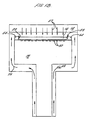
Fig. 1A is a vertical, cross-sectional view of one embodiment of a
simplified chemical vapor deposition apparatus according to the present invention;
Fig. 1B is a vertical, cross-sectional view of one embodiment of a
resistively heated susceptor used in the chamber of Fig. 1 to secure a substrate being
processed in chamber;
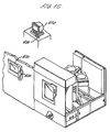
Fig. 1C is a simplified diagram of system monitor and CVD system 100
in a multi-chamber system, which may include one or more chambers;
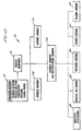
Fig. 1D shows an illustrative block diagram of the hierarchical control
structure of the system control software, computer program 170, according to a specific
embodiment;
Fig. 2 is a flowchart illustrating the steps of one embodiment of the
present invention;
Fig. 3A is a simplified cross-sectional view of a HAR contact gap for
which embodiments of the present invention may be used to fill;
Fig. 3B is an enlarged view of the gap shown in Fig. 3A partially filled
with titanium and titanium nitride layers; and
Fig. 4 is a chart illustrating the effect of the hydrogen:argon flow ratio
used during deposition of a tungsten nucleation layer on the fluorine concentration of a
W/TiN/Ti film stack; and
Figs. 5A and 5B are SIMS depth profiles comparing the fluorine
concentration in W/TiN/Ti film stacks having tungsten layers deposited with and
without the benefits of deposition techniques according to the embodiments of the
present invention.
I. Introduction
Embodiments of the present invention allow for deposition of an
improved tungsten film by flowing a relatively high ratio of hydrogen to argon into the
chamber during deposition of a tungsten nucleation layer and keeping the partial
pressure of WF6 relatively low. The present inventors discovered that when a tungsten
film is deposited in this manner, less fluorine contamination results in the underlying
TiN/Ti film stack than it does if the tungsten film is deposited according to a previously
known tungsten CVD process. Films deposited by the method of the present invention
are suitable for use in the fabrication of integrated circuits having feature sizes of 0.25
microns or less and can be used to completely fill vias and contacts having an aspect
ratio of 8:1 with a 0.25 µm diameter opening in a void free manner. Also, the present
invention can be used to deposit tungsten films in CVD chambers of conventional
design.
II. Exemplary CVD Reactor Chamber
Figs. 1A and 1B illustrate one embodiment of a parallel plate, cold-wall
chemical vapor deposition system 10 having a vacuum chamber 12 in which the
tungsten film according to the present invention can be deposited. CVD System 10
contains a gas distribution manifold 14 for dispersing deposition gases to a wafer 16
that rests on a resistively-heated pedestal 18.
Chamber 12 may be part of a vacuum processing system having multiple
processing chambers connected to a central transfer chamber and serviced by a robot.
Substrate 16 is brought into chamber 12 by a robot blade through a slit valve in a
sidewall of the chamber (not shown). Pedestal 18 is moveable vertically by means of a
motor 20. Substrate 16 is brought into the chamber when pedestal 18 is in a first
position 13 opposite the slit valve. At position 13, substrate 16 is supported initially by
a set of pins 22 that pass through and are coupled to susceptor 18. Pins 22 are driven
by a single motor assembly.
As the pedestal is brought to a processing position 32 opposite gas
distribution manifold 14 as shown by the dotted line, pins 22 sink into pedestal 18 and
substrate 16 is deposited onto the pedestal. Once positioned on pedestal 18, substrate
16 is affixed to the pedestal by a vacuum clamping system (shown in Fig. 1B as
grooves 50).
As it moves upward toward processing position 32, substrate 16 contacts
purge guide 54, which centers the substrate on the pedestal. Edge purge gases 23 are
flowed through purge guide 54 across the edge of substrate 16 to prevent deposition
gases from contacting the edge and backside of the substrate. Purge gases 25 are also
flowed around heater/pedestal 18 to minimize deposition on an around the
heater/pedestal. These purge gases are supplied from a purge line (Fig. 1A, 24) and are
also employed to protect stainless steel bellows 26 from damage by corrosive gases
introduced into the chamber during processing.
Deposition and carrier gases are supplied to a deposition zone of the
chamber through gas lines 19 to manifold 14 in response to the control of valves 17.
During processing, gas supplied to manifold 14 is distributed uniformly across the
surface of the substrate as shown by arrows 27. Spent processing gases and by-product
gases are exhausted from the chamber by means of exhaust system 36. The rate at
which gases are released through exhaust system 36 into an exhaust line is controlled
by a throttle valve (not shown). During deposition, a second purge gas through gas
channels in the susceptor (not shown) and feed line 38 feeds purge gas against the edge
of wafer 16 as previously described. An RF power supply 48 can be coupled to
manifold 14 to provide for plasma-enhanced CVD (PECVD) cleaning of the chamber.
The throttle valve, gas supply valves 17, motor 20, resistive heater
coupled to susceptor 18, RF power supply 48 and other aspects of CVD system 10 are
controlled by a processor 42 over control lines 44 (only some of which are shown).
Processor 42 operates under the control of a computer program stored in a computer-readable
medium such as a memory 46. The computer program dictates the
temperature, chamber pressure, timing, mixture of gases, RF power levels, susceptor
position, and other parameters of a particular process.
In a preferred embodiment, the system controller includes a hard disk
drive (memory 46 a floppy disk drive and a processor 42. The processor contains a
single-board computer (SBC), analog and digital input/output boards, interface boards
and stepper motor controller boards. Various parts of CVD system 10 conform to the
Versa Modular European (VME) standard which defines board, card cage, and
connector dimensions and types. The VME standard also defines the bus structure as
having a 16-bit data bus and a 24-bit address bus.
System controller 42 controls all of the activities of the CVD machine.
The system controller executes system control software, which is a computer program
stored in a computer-readable medium such as a memory 46. Preferably, memory 46 is
a hard disk drive, but memory 46 may also be other kinds of memory. The computer
program includes sets of instructions that dictate the timing, mixture of gases, chamber
pressure, chamber temperature, RF power levels, susceptor position, and other
parameters of a particular process. Other computer programs stored on other memory
devices including, for example, a floppy disk or other another appropriate drive, may
also be used to operate controller 42.
The interface between a user and controller 42 is via a CRT monitor 60a
and light pen 60b, shown in Fig. 1C which is a simplified diagram of the system
monitor and CVD system 10 in a substrate processing system, which may include one
or more chambers. In the preferred embodiment two monitors 60a are used, one
mounted in the clean room wall for the operators and the other behind the wall for the
service technicians. The monitors 60a simultaneously display the same information,
but only one light pen 60b is enabled. A light sensor in the tip of light pen 60b detects
light emitted by CRT display. To select a particular screen or function, the operator
touches a designated area of the display screen and pushes the button on the pen 60b.
The touched area changes its highlighted color, or a new menu or screen is displayed,
confirming communication between the light pen and the display screen. Other
devices, such as a keyboard, mouse, or other pointing or communication device, may
be used instead of or in addition to light pen 60b to allow the user to communicate with
controller 42.
The process for depositing the film can be implemented using a
computer program product that is executed by controller 42. The computer program
code can be written in any conventional computer readable programming language: for
example, 68000 assembly language, C, C++, Pascal, Fortran or others. Suitable
program code is entered into a single file, or multiple files, using a conventional text
editor, and stored or embodied in a computer usable medium, such as a memory system
of the computer. If the entered code text is in a high level language, the code is
compiled, and the resultant compiler code is then linked with an object code of
precompiled Windows™ library routines. To execute the linked, compiled object code
the system user invokes the object code, causing the computer system to load the code
in memory. The CPU then reads and executes the code to perform the tasks identified
in the program.
Fig. 1D is an illustrative block diagram of the hierarchical control
structure of the system control software, computer program 70, according to a specific
embodiment. Using the light pen interface, a user enters a process set number and
process chamber number into a process selector subroutine 73 in response to menus or
screens displayed on the CRT monitor. The process sets are predetermined sets of
process parameters necessary to carry out specified processes, and are identified by
predefined set numbers. The process selector subroutine 73 identifies (i) the desired
process chamber and (ii) the desired set of process parameters needed to operate the
process chamber for performing the desired process. The process parameters for
performing a specific process relate to process conditions such as, for example, process
gas composition and flow rates, temperature, pressure, plasma conditions such as RF
power levels and the low frequency RF frequency, cooling gas pressure, and chamber
wall temperature. These parameters are provided to the user in the form of a recipe,
and are entered utilizing the light pen/CRT monitor interface.
The signals for monitoring the process are provided by the analog and
digital input boards of the system controller, and the signals for controlling the process
are output on the analog and digital output boards of CVD system 10.
A process sequencer subroutine 75 comprises program code for
accepting the identified process chamber and set of process parameters from the
process selector subroutine 73, and for controlling operation of the various process
chambers. Multiple users can enter process set numbers and process chamber numbers,
or a user can enter multiple process set numbers and process chamber numbers, so the
sequencer subroutine 75 operates to schedule the selected processes in the desired
sequence. Preferably, the sequencer subroutine 75 includes a program code to perform
the steps of (i) monitoring the operation of the process chambers to determine if the
chambers are being used, (ii) determining what processes are being carried out in the
chambers being used, and (iii) executing the desired process based on availability of a
process chamber and type of process to be carried out. Conventional methods of
monitoring the process chambers can be used, such as polling. When scheduling which
process is to be executed, sequencer subroutine 75 takes into consideration the present
condition of the process chamber being used in comparison with the desired process
conditions for a selected process, or the "age" of each particular user entered request, or
any other relevant factor a system programmer desires to include for determining
scheduling priorities.
Once the sequencer subroutine 75 determines which process chamber
and process set combination is going to be executed next, the sequencer subroutine 75
initiates execution of the process set by passing the particular process set parameters to
a chamber manager subroutine 77a-c, which controls multiple processing tasks in a
process chamber 12 according to the process set determined by the sequencer
subroutine 75. For example, the chamber manager subroutine 77a comprises program
code for controlling CVD process operations in the process chamber 12. The chamber
manager subroutine 77 also controls execution of various chamber component
subroutines that control operation of the chamber components necessary to carry out
the selected process set. Examples of chamber component subroutines are substrate
positioning subroutine 80, process gas control subroutine 83, pressure control
subroutine 85, heater control subroutine 87 and plasma control subroutine 90 in some
embodiments. A person having ordinary skill in the art will readily recognize that other
chamber control subroutines can be included depending on what processes are to be
performed in the process chamber 12. In operation, the chamber manager subroutine
77a selectively schedules or calls the process component subroutines in accordance
with the particular process set being executed. The chamber manager subroutine 77a
schedules the process component subroutines much like the sequencer subroutine 75
schedules which process chamber 12 and process set are to be executed next.
Typically, the chamber manager subroutine 77a includes steps of monitoring the
various chamber components, determining which components need to be operated
based on the process parameters for the process set to be executed, and causing
execution of a chamber component subroutine responsive to the monitoring and
determining steps.
Operation of particular chamber component subroutines will now be
described with reference to Fig. 1D. The substrate positioning subroutine 80 comprises
program code for controlling chamber components that are used to load the substrate
onto pedestal 18 and, optionally, to lift the substrate to a desired height in the chamber
12 to control the spacing between the substrate and the gas distribution manifold 14.
When a substrate is loaded into the process chamber 12, pedestal 18 is lowered to
receive the substrate, and thereafter, the pedestal 18 is raised to the desired height in the
chamber, to maintain the substrate at a first distance or spacing from the gas
distribution manifold during the CVD process. In operation, the substrate positioning
subroutine 80 controls movement of pedestal 18 in response to process set parameters
related to the support height that are transferred from the chamber manager subroutine
77a.
The process gas control subroutine 83 has program code for controlling
process gas composition and flow rates. The process gas control subroutine 83 controls
the open/close position of the safety shut-off valves, and also ramps up/down the mass
flow controllers to obtain the desired gas flow rate. The process gas control subroutine
83 is invoked by the chamber manager subroutine 77a, as are all chamber component
subroutines, and receives from the chamber manager subroutine process parameters
related to the desired gas flow rates. Typically, the process gas control subroutine 83
operates by opening the gas supply lines and repeatedly (i) reading the necessary mass
flow controllers. (ii) comparing the readings to the desired flow rates received from the
chamber manager subroutine 77a, and (iii) adjusting the flow rates of the gas supply
lines as necessary. Furthermore, the process gas control subroutine 83 includes steps to
monitor the gas flow rates for unsafe rates and for activating the safety shut-off valves
when an unsafe condition is detected.
In some processes, an inert gas such as helium or argon is flowed into
the chamber 12 to stabilize the pressure in the chamber before reactive process gases
are introduced. For these processes, the process gas control subroutine 83 is
programmed to include steps that flow the inert gas into the chamber 12 for an amount
of time necessary to stabilize the pressure in the chamber, and then the steps described
above would be carried out.
The pressure control subroutine 85 comprises program code for
controlling the pressure in the chamber 12 by regulating the size of the opening of the
throttle valve in the exhaust system of the chamber. The size of the opening of the
throttle valve is set to control the chamber pressure to the desired level in relation to the
total process gas flow, size of the process chamber, and pumping setpoint pressure for
the exhaust system. When the pressure control subroutine 85 is invoked, the desired, or
target, pressure level is received as a parameter from the chamber manager subroutine
77a. The pressure control subroutine 85 operates to measure the pressure in the
chamber 12 by reading one or more conventional pressure manometers connected to the
chamber, to compare the measure value(s) to the target pressure, to obtain PID
(proportional, integral, and differential) values from a stored pressure table
corresponding to the target pressure, and to adjust the throttle valve according to the
PID values obtained from the pressure table. Alternatively, the pressure control
subroutine 85 can be written to open or close the throttle valve to a particular opening
size to regulate the chamber 12 to the desired pressure.
The heater control subroutine 87 comprises program code for controlling
the current to a heating unit that is used to heat the substrate 20. The heater control
subroutine 87 is also invoked by the chamber manager subroutine 77a and receives a
target, or set-point, temperature parameter. The heater control subroutine 87 measures
the temperature by measuring voltage output of a thermocouple located in pedestal 12,
comparing the measured temperature to the set-point temperature, and increasing or
decreasing current applied to the heating unit to obtain the set-point temperature. The
temperature is obtained from the measured voltage by looking up the corresponding
temperature in a stored conversion table, or by calculating the temperature using a
fourth-order polynomial. When an embedded loop is used to heat susceptor 18 the
heater control subroutine 87 gradually controls a ramp up/down of current applied to
the loop. Additionally, a built-in fail-safe mode can be included to detect process
safety compliance, and can shut down operation of the heating unit if the process
chamber 12 is not properly set up.
In some embodiments, chamber 12 is outfitted with an RF power supply
48 that is used for chamber cleaning or other operations. When a chamber cleaning
plasma process is employed, plasma control subroutine 90 comprises program code for
setting the frequency RF power levels applied to the process electrodes in the chamber
12. Similar to the previously described chamber component subroutines, the plasma
control subroutine 90 is invoked by the chamber manager subroutine 77a.
The above CVD system description is mainly for illustrative purposes
and should not be considered as limiting the scope of the present invention. Variations
of the above described system, such as variations of pedestal design, heater design,
location of RF power connections and others are possible. The method for depositing a
tungsten layer according to the present invention is not limited to any specific
processing apparatus.
III. Depositing Tungsten Films
The method of the present invention may be employed to deposit
improved tungsten films in a substrate processing chamber, such as the exemplary
CVD chamber described above. Fig. 2 illustrates one embodiment of the invention that
is used to deposit a tungsten film over a semiconductor substrate. The process is for
exemplary purposes and is not intended to limit the scope of the claims of the present
invention. Where applicable, reference numbers in the description below are used to
refer to appropriate components of the exemplary chamber of Figs. 1A-1D. This
process may be implemented and controlled using a computer program stored in the
memory 46 of CVD system 10.
The embodiment of the invention shown in Fig. 2 includes a silane soak
step 100 in which a silane gas, such as dichlorosilane (SiCl2H2) or monosilane (SiH4),
and a carrier gas, such as argon and hydrogen, are flowed into chamber 12 for between
5 and 30 seconds to provide silane adsorption on the TiN surface before nucleation. In
one particular embodiment, silane soak step 100 flows 75 sccm of SiH4 into chamber
12 along with 500 sccm of H2 and 1000 sccm of argon for 10 seconds at a chamber
pressure of 90 Torr.
After completion of silane soak step 100, a nucleation step 105 is
performed. Nucleation step 105 flows a process gas including WF6, SiH4, H2, argon
and optionally nitrogen into chamber 12 to grow a thin tungsten layer that acts as a
growth site for subsequent tungsten film. Generally the nucleation gas is flowed into
the chamber for between 4 to 60 seconds. During this time the pedestal temperature is
set to between 350 and 475°C and chamber pressure is set to a level between 1 and 50
Torr. As discussed in more detail below, the present inventors have discovered that
flowing H2 and argon into chamber 12 in a ratio of at least 1.5:1 (H2:Ar) and setting gas
flows such that the partial pressure of WF6 is less than or equal to 0.5 Torr during step
105 results in less fluorine being incorporated into the tungsten layer than would result
if lower H2:Ar ratios were employed. Lower levels of fluorine in the tungsten layer, in
turn, results in improved electrical characteristics of transistors formed on substrate 16.
Bulk deposition step 110 then completes deposition of the tungsten layer
by flowing a process gas including WF6, H2, argon and optionally N2 into chamber 12.
Chamber pressure during step 110 is maintained between 50 and 760 Torr while the
pedestal temperature is set to between 350 and 475°C. The length of the bulk
deposition step depends on the desired thickness of the tungsten film. While not
necessary in all embodiments, some embodiments of the invention also employ a H2:Ar
flow ratio of at least 1.5:1 in bulk deposition step 110.
Tungsten films deposited according to the above process can achieve
void free (100% step coverage) of HAR, narrow diameter vias (e.g., 0.25 µm vias
having an aspect ratio of 8:1). The films also have reduced fluorine content as
compared to films deposited using a H2:Ar flow ratio of less than 1.5:1 in the
nucleation step. Minimizing fluorine content in the tungsten film is particularly useful
since fluorine from the tungsten film can diffuse into a neighboring titanium nitride
and/or titanium layer thereby increasing the resistance of those layers.
In order to better appreciate the fluorine diffusion problem, reference is
made to Figs. 3A and 3B, which are simplified cross-sectional views of an integrated
circuit having a tungsten contact. In Fig. 3A, an HAR gap 120 has been etched in a
dielectric layer 122, such as a borophosphorus silicate glass (BPSG) layer, deposited
over a transistor 124 formed in a substrate 126. Transistor 124 includes a gate 128 and
source/drain regions 130. Electrical contact is made to source/drain regions 130 in
HAR gap 120 by depositing a W/TiN/Ti film stack as is known to those of ordinary
skill in the art. Because of the shrinking transistor size and the use of structures such as
tall, three dimensional capacitors in dynamic access memories (DRAMs), some HAR
gaps 120 in modern integrated circuits have increased depth to diameter (or aspect
ratios) measurements than such gaps did in previous generations of integrated circuits.
Fig. 3B is an enlarged view of HAR gap 120 shown in Fig. 3A. As
shown in Fig. 3B, deposition of a titanium contact layer 132 and a titanium nitride
diffusion barrier layer 134 precedes deposition of a tungsten film within the gap and
further narrows the opening of gap 120 prior to tungsten deposition. Fluorine from a
CVD tungsten film 136 deposited within gap 120 can diffuse into the titanium nitride
layer 134 and titanium contact layer 132 during deposition of the tungsten layer or
during subsequent processing. Such fluorine diffusion may increase the resistivity of
the TiN/Ti layers and thereby increase the resistance of the contact. The inventors have
found that even a small increase in fluorine concentration in the TiN/Ti layers can have
a significant impact on the electrical characteristics of the contact. This in turn may
result in an adverse impact on device yield because of failures due to the high contact
resistance. For example, in a DRAM circuit the increased resistance may result in an
overall decrease in circuit speed such that the timing requirements for accessing or
refreshing individual cells cannot be met. The inventors have also found that because
of the diffusivity of fluorine in tungsten (measured to be approximately
4 × 10-14 cm2/sec at 425°C) the majority of fluorine that migrates to the TiN/Ti layers
comes from tungsten nucleation layer 138.
Realizing the significance that reducing fluorine concentration in the
tungsten film may have on device performance, the inventors developed the method
discussed above with respect to Fig. 2 to minimize fluorine incorporation into the
tungsten film and thereby minimize the source of fluorine diffusion into the titanium
nitride/titanium layers. One way to reduce fluorine levels in the tungsten film is to
employ a WF6 to SiH4 ratio of around 1:1. Tungsten film step coverage is adversely
affected at WF6:SiH4 ratios this low, however, and the deposited film may become
silicon-rich and exhibit low reflectivity. For these and other reason it is preferred that
the WF6:SiH4 ratio be between about 1.5:1 and 4:1 and preferably be between 2:1 and
3:1 inclusive.
The inventors thus developed a different method of reducing fluorine
content. This goal was accomplished by increasing the flow of molecular hydrogen
used during the deposition of the tungsten nucleation layer. In one embodiment, the
ratio of H2 to argon is at least 1.5:1 while the partial pressure of WF6 is less than or
equal to 0.5 Torr. It is desirable to have a total gas flow of H2 and Ar sufficiently high
so that WF6 partial pressure is 0.5 Torr or less in order to achieve high uniformity and
reduce fluorine attack on the underlying layer during the tungsten deposition process as
well as to reduce the fluorine attack on chamber components. In other embodiments,
the ratio of H2 to Argon is preferably at least 2:1.
The inventors unexpectedly discovered that when a tungsten nucleation
layer was deposited over a TiN/Ti film stack under these conditions, the contact
resistance was improved as compared to the contact resistance measured when the
tungsten nucleation layer was deposited at lower H2 to Ar ratios. The inventors
discovered this to be the case under all tested deposition temperatures (from 400°C to
475°C) but noticed that contact resistance decreased the most at the higher deposition
temperatures.
In order to reach the above conclusions, the inventors ran numerous tests
and studies comparing the fluorine concentration of W/TiN/Ti film stacks having
tungsten layers deposited with and without the benefits of the present invention. One
of these tests, set forth in Table 1 and described below, was performed on 200 mm
silicon (100) wafers having a W/TiN/Ti film stack deposited over a 3000 Å thermally
grown oxide film grown thereon. The W/TiN/Ti film stack was formed as follows.
First, the oxidized wafers were loaded into an Applied Materials Endura™ cluster tool
and deposited with 750 Å of titanium by biased sputtering, followed by 80 Å of TiN by
metalorganic chemical vapor deposition (MOCVD). The source gas for TiN was
tetrakis demethylamido titanium (TDMat), and the film was plasma treated subject to a
plasma densification treatment using 250 W of 13.56 MHz radio frequency to form a
plasma from N
2 to densify the film and reduce the concentration of organic
contaminants. After plasma treatment, the TiN film was approximately 50 Å thick.
The wafers were then loaded into an Applied Materials WxZ Centura™ tool for
tungsten deposition. Prior to tungsten nucleation film deposition, the wafers were
exposed to an
in situ SiH
4 treatment step resulting in SiH
4 adsorption on the TiN
surface. This SiH
4 exposure provides for a more homogeneous tungsten deposition, as
previously described. Nucleation film deposition was performed at a pressure of 30
Torr and a wafer pedestal temperature of 475°C (wafer temperature approximately
10-15°C less). The WF
6 and SiH
4 flows were 30 and 10 standard cubic centimeters per
minute (sccm), respectively. Deposition times for the wafers shown were adjusted to
produce approximately 500 Å of tungsten nucleation film on all wafers.
| EXPERIMENTS VARYING THE RATIO OF H2 FLOW TO AR FLOW |
| Wafer | WF6:SiH4 (sccm) | H2 (sccm) | Ar (sccm) | H2/Ar ratio | Total H2/Ar flow (seem) | WF6 partial pressure (Torr) |
| 1 | 30:10 | 500 | 2500 | .2:1 | 3000 | 0.3 |
| 2 | 30:10 | 1000 | 2000 | .5:1 | 3000 | 0.3 |
| 3 | 30:10 | 1500 | 1500 | 1:1 | 3000 | 0.3 |
| 4 | 30:10 | 2000 | 1000 | 2:1 | 3000 | 0.3 |
| 5 | 30:10 | 2250 | 750 | 3:1 | 3000 | 0.3 |
| 6 | 30:10 | 2500 | 500 | 5:1 | 3000 | 0.3 |
As shown in Table 1, these experiments varied the H2:Ar flow ratio from
0.2:1 to 5:1 while the total H2 + Ar flow was kept at 3000 sccm during deposition of the
tungsten nucleation layer. After deposition of the tungsten layer, the fluorine
concentration in the TiN/Ti film stack was measured. The results of these
measurements are shown in Fig. 4.
As shown in Fig. 4, the fluorine dose in the TiN/Ti film stack over
which the tungsten layers detailed in Table 1 is deposited decreases dramatically as an
initial amount of hydrogen is included in the deposition gas, then increases somewhat at
a ratio of 1:1 and decreases again as the H2:Ar flow ratio reaches about 1.5:1. The
fluorine dose levels obtained at H2:Ar flow levels of 1.5:1 and higher result in
significantly improved electrical characteristics of the TiN/Ti contact structure and
higher product yield. As used herein, fluorine dose is calculated from a SIMS plot by
integrating the area beneath the F concentration curve as is known to those of skill in
the art. The actual fluorine dose is thus specific to the chosen TiN/Ti film stack,
nucleation film thickness, and other variables.
Figs. 5A and 5B show representative SIMS depth profiles from wafers 1
and 4 in the Table 1 set of experiments. Depth profile analysis for these figures was
done by sputtering SIMS using quadrapole spectrometer analysis. Sputtering was done
by 3 keV Cs+ beam. Film thickness was checked by cross sectional scanning electron
microscopy (SEM). As evident from comparison of Fig. 5A to Fig. 5B, considerably
less fluorine is incorporated into the TiN/Ti film stack represented in Fig. 5B. Step
coverage of tungsten nucleation films using the deposition conditions for wafers 4-6 in
Table 1 was checked on wafers with 0.3 µm diameter vias etched into 2.4 µm thick
oxide films (8:1 aspect ratio) with 50 Å TiN/250 Å Ti film stacks and determined to be
100%.
Other experiments performed by the inventors confirmed these results.
From some of these experiments the inventors were also able to determine that
increasing the total H2 + Ar flows above 3000 sccm resulted in further improvements to
fluorine dose. For example, improvements were found in a 30 sccm WF6, 15 sccm
SiH4, 4:1 H2:Ar flow ratio process when total H2 + Ar flow was increased to 5000 sccm
and to 10,000 sccm. Specifically, the concentration of fluorine in the tungsten
nucleation film is reduced by half when 10,000 sccm of H2 + Ar is flowed (2 × 10¹⁹
atoms/cm3) compared with 2,500 sccm (4 × 10¹⁹ atoms/cm3). Fluorine penetration into
the TiN/Ti films shows similar decreases with increasing H2 + Ar flows.
In summary, based on the above test results and other work performed
by the inventors, the inventors have determine that fluorine content in a TiN/Ti film
stack underlying a tungsten layer can be reduced by setting H2 and Ar flow so that the
ratio of H2:Ar is at least 1.5:1 and the partial pressure of WF6 is less than or equal to 0.5
Torr. The reduction is more pronounced at higher tungsten deposition temperatures
such as 475°C but can still have a noticeable impact on device yield at lower tungsten
deposition temperatures such as 400°C.
The process parameters set forth above with respect to the preferred
embodiments are optimized for one particular deposition process run in a resistively
heated WxZ chamber outfitted for 200 mm wafers and manufactured by Applied
Materials. In addition to varying processing parameters described above to deposit
tungsten layers according to specific applications, a person of ordinary skill in the art
will recognize that these preferred parameters are in part chamber specific and will vary
if chambers of other design and/or volume are employed. It should also be noted that
various purge gases may be flowed into the substrate processing chamber during
deposition of the tungsten layer as is known to those of skill in the art. Such purge
gases may include argon but they are not intended to be calculated into the 1.5:1 H2:Ar
ratio set forth above. Instead, that ratio is calculated based on deposition and carrier
gases; it does not include purge gases.
The parameters listed in the above preferred processes and the above-described
experiments should not be limiting to the claims as described herein. One of
ordinary skill in the art can also use parameters and conditions other than those
described with respect to the preferred embodiment. As such, the above description is
illustrative and not restrictive. For example, while not described above, a person of
ordinary skill in the art will appreciate that various intermediary steps can be included
before and after each of steps 100, 105 and 110 to optimize film characteristics such as
uniformity, reflectivity and film stress. For example, substrate 16 can be heated to a
desired temperature in the presence of an inert gas prior to step 100. Similarly,
chamber 12 can be brought to the desired pressure level of step 105 or step 110 while
flowing argon and H2 into the chamber without flowing WF6. Also, WF6 can be purged
from chamber 12 after the bulk deposition step by a flow of argon and H2. Also, other
process temperature and pressure values and other gas flow rates can be employed.
Similarly, other variations in a tungsten deposition process can be made
without departing from the scope of the invention. For example, some embodiments of
the present invention do not include silane soak step 100. Also, other embodiments
may include a multiple step nucleation process in which one step deposits a tungsten
nucleation film as described above but not all steps. The scope of the invention should,
therefore, be determined not with reference to the above description, but instead should
be determined with reference to the appended claims along with their full scope of
equivalents.