Technical Field
-
This invention relates to a manufacturing process for a
semiconductor wafer (hereinafter also referred to as a "wafer")
including surface grinding, followed by planarization or polishing.
Background of Art
-
In a manufacturing process for a semiconductor wafer of this
kind, a semiconductor wafer has been surface-ground according to a
process described below, shown in FIG. 10(a)(b)(c) and thereafter, a
single side surface or double side surfaces thereof are processed for
planarization according to a CMP (Chemical Mechanical Polishing)
method, or a PACE (Plasma Assisted Chemical Etching) method (for
example, see JP 2565617) for purposes of removal of a work damage
layer caused by the grinding, and improvements on flatness and
smoothness.
- (1) First, a chuck table 12 for fixing a semiconductor wafer W
thereon rotates on its rotation axis 12a with a prescribed slight tilt
angle to the rotation axis 14a of a rotary shaft 14 of a cup shaped
grinding wheel (hereinafter also simply referred to as a "grinding
wheel") 16. Then, the grinding wheel 16 in rotation moves down and
is into contact with the chuck table 12 to grind the chuck table 12
(FIG. 10(a)), with the result that a grinding finished surface of the
chuck table 12 assumes an outwardly extending circular cone surface
having a vertical angle (180 - 2) with a vertex thereof being the
rotation axis of the chuck table 12.
- (2) Then, a semiconductor wafer W is fixed on the surface
ground chuck table 12 and the chuck table 12 is forced to rotate (FIG.
10(b)).
- (3) Furthermore, the grinding wheel 16 moves down to a
surface of the semiconductor wafer W and is into contact with the
wafer W, thereby the wafer W being surface-ground (FIG.10(c)).
-
-
In recent years, a trend that surface grinding, as a
processing method to obtain higher flatness, is introduced into a
wafer processing step has been increasingly enhanced due to the
demand for higher flatness of a semiconductor wafer. In the
surface-grinding step of the semiconductor wafer, as shown in FIG.
10(a) to (c), the grinding is performed such that the cup shaped
grinding wheel 16 cuts into the wafer W at an outer peripheral edge
thereof and moves away from the wafer at a central portion, wherein
the grinding proceeds while the grinding wheel 16 keeps in contact
with the wafer over a length corresponding to a radius of the wafer W.
-
As schematically shown in FIG. 11, a removal by grinding is
low due to a surface slipping phenomenon from elasticity of the
grinding wheel 16 at a start position for cutting-in of the grinding
wheel 16 in contacting the wafer as a work and as a result, a grinding
finished surface comes to have a slight rise at the start position,
while at a terminating position for cutting, the grinding finished
surface comes to have a recess because a grinding removal increases
due to rapid reduction in resistance to cutting. These rise and recess
characteristic of a finished surface obtained by surface-grinding have
been obstacles against manufacturing a wafer having higher flatness.
-
For example, in the case where surface-grinding is effected
using a resinoid bonded cup shaped grinding wheel including diamond
abrasive powder and furthermore, the grinding is performed toward
the center of the wafer from an outer peripheral edge thereof, as was
in the prior art, such that the grinding wheel cuts into the wafer at
the outer peripheral edge thereof and moves away from the wafer at
the center thereof, there occur a recess in the vicinity of the center of
the surface-ground wafer, of the order of 2 to 10 mm in diameter and
of the order of 0.2 to 0.5 µm in depth, and a rise of the same order as
the recess in size in the outer peripheral edge portion thereof.
-
The surface-ground wafer proceeds into a planarization or
polishing step to come next, where a work damage layer on the
surface-ground surface of the wafer caused by the surface-grinding is
removed and the above described rise and recess portions are
corrected to achieve increased flatness and enhanced smoothness.
-
In a polishing method using a polishing cloth, that is a CMP
method, which is currently a main stream as a planarization or
polishing method, the polishing cloth is made of a soft material,
therefore, there is a tendency that a polishing surface of the cloth
follows geometric features of a to-be-polished surface of a work and as
a result, a polishing action is exercised to even a recess portion in the
vicinity of the center of the wafer, therefore, correction of the recess
portion is hard to be effected. In contrast to this, a polishing action
is easy to act at a rise portion occurring locally in the outer
peripheral edge portion, therefore, a rise in the outer peripheral edge
portion is corrected.
-
On the other hand, in a PACE method newly developed for
planarization, stock can be removed from a to-be-ground surface
locally to a prescribed depth by an etching action of a plasma;
therefore, a surface material is removed from part other than the
recess portion, whereby flatness all over the surface can be improved.
-
The invention has been made in light of the above described
prior art problem and it is accordingly an object of the invention to
provide a manufacturing process for a semiconductor wafer capable of
manufacturing the semiconductor wafer having higher flatness
efficiently from a wafer work having passed through a surface
grinding step by suppressing the above-noted reductions in flatness
occurring in the vicinity of the center of the wafer work and in the
outer peripheral edge portion thereof as much as possible and further,
enabling correction of the reductions in flatness for planarization in a
planarization or polishing step with ease.
Disclosure of the Invention
-
In order to solve the above problem, a first aspect of the
invention is directed to a manufacturing process for a semiconductor
wafer wherein when the semiconductor wafer is surface ground using
a cup shaped grinding wheel, the semiconductor wafer is ground
toward the center thereof such that the cup shaped grinding wheel
cuts into the semiconductor wafer at an outer peripheral edge thereof
and moves away from the semiconductor wafer at a central portion
thereof and the ground semiconductor wafer is planarized according
to a PACE method.
-
That is, since in a surface grinding operation, the grinding
wheel cuts into the semiconductor wafer at the outer peripheral edge
portion and moves away from the semiconductor wafer at the central
portion, there occur a rise in the outer peripheral edge portion of a
finish surface of the wafer after the grinding and a recess in the
central portion thereof. However, by use of the PACE method, there
is corrected the recess in the central portion of the wafer, which in
the prior art was difficult to be corrected by means of a method for
polishing the wafer using a CMP method after the surface grinding,
thereby enabling manufacture of a polished wafer having higher
flatness.
-
A surface of the semiconductor wafer which has been
planarized using the PACE method has very fine rises and recesses
thereon remaining after the planarization; therefore, it is desirable to
improve flatness and smoothness of the surface by further polishing
the surface using a CMP method.
-
A method to force the grinding wheel to cut into the
semiconductor wafer at the outer peripheral edge thereof can be
performed such that rotation directions of the semiconductor wafer
and the grinding wheel can be either of the same sense as each other
or of the opposite senses from each other.
-
A chuck table, as described above, has a finished surface of a
slightly inclined circular cone whose vertex is on the rotation axis of
the chuck table. The wafer is held on the chuck table and surface
grinding is performed so as to act over a radius of the wafer surface
while holding a state of the wafer in which a central portion of a
to-be-ground surface of the wafer slightly protrudes from a plane
including a grinding surface of the grinding wheel; therefore, an angle
formed between the rotation axis of the rotary shaft of the grinding
wheel and the rotation axis of the chuck table is necessary to be
adjusted according to whether rotation directions of the
semiconductor wafer, that is the chuck table, and the grinding wheel
are the same sense as each other, or the opposite sense from each
other.
-
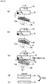
That is, as shown in FIG. 5, in the case where rotation
directions of the grinding wheel and the chuck table are the same
sense as each other, the rotation axis of the chuck table has to be
inclined by along a clockwise direction, as shown in the figure, to
the rotation axis of the rotary shaft of the grinding wheel, while to
the contrary, in the case of FIG. 6 where rotation directions of the
grinding wheel and the chuck table are opposite from each other, the
rotation axis of the chuck table has to be inclined by along a
counterclockwise direction to the rotation axis of the rotary shaft of
the grinding wheel, whereby grinding can be performed such that the
grinding wheel is cut into the wafer at the outer peripheral edge
portion and moves away from the wafer at the central portion.
-
A second aspect of the present invention is directed to a
manufacturing process for a semiconductor wafer wherein when the
semiconductor wafer is surface ground using a cup shaped grinding
wheel, the semiconductor wafer is ground toward the outer periphery
thereof such that the cup shaped grinding wheel cuts into the
semiconductor wafer at the center thereof and moves away from the
semiconductor wafer at an outer peripheral edge thereof and the thus
ground semiconductor wafer is planarized by means of a CMP method.
-
That is, in this case, since when the semiconductor wafer is
surface ground, the grinding wheel cuts into the semiconductor wafer
at the center thereof and moves away from the semiconductor wafer
at an outer peripheral edge portion thereof, there occur a rise in the
central portion of the grinding finished surface of the wafer and sag
in the outer peripheral edge portion. Hence, in this case, since the
rise in the central portion can be corrected by a polishing action of the
CMP method with ease, the prior art problem is solved and thus a
wafer having high flatness all over the polishing finished surface
thereof can be manufactured. Note that since the wafer rotates
about a rotation axis passing substantially through the center of a
ground surface being held by a chuck, a peripheral velocity due to
rotation thereof is larger at a point on the ground surface closer to the
outer periphery; therefore, a contact time of the ground surface of the
wafer per unit area of the surface with the grinding wheel in the
outer peripheral edge portion is shorter and accordingly an edge sag
in the outer peripheral edge portion due to grinding is relatively
small. Since in a CMP method the surface of a polishing cloth
deforms in conformity with geometrical features of the ground surface
of the wafer, an edge sag in the outer peripheral edge portion of the
polished surface of the wafer has almost no difference in dimension
from that under a polishing action of a normal CMP method.
-
A method to force the grinding wheel to cut into the
semiconductor wafer at the center thereof can be performed such that
rotation directions of the semiconductor wafer and the grinding wheel
can be either of the same sense as each other or of the opposite senses
from each other.
-
In order that the grinding wheel cuts into the wafer at the
center thereof and moves away from the wafer at the outer peripheral
portion thereof, it is necessary to adjust an angle of the rotation
axis of the chuck table to the rotation axis of the rotary shaft of the
grinding wheel according to whether rotation directions of the chuck
table and the grinding wheel is of the same sense or of the opposite
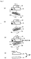
senses. The purpose can be achieved such that in the case of the
same sense the rotation axis of the chuck table is, as shown in FIG. 7,
inclined counterclockwise by relative to the rotation axis of the
rotary shaft of the grinding wheel, while on the other hand, in the
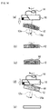
case of the opposite senses the rotation axis of the chuck table is, as
shown in FIG. 8, inclined clockwise by relative to the rotation axis
of the rotary shaft of the grinding wheel.
-
Moreover, it has been found that in order that, as is in a
method of the invention, a wafer with extremely high flatness is
manufactured with good efficiency by combining surface grinding with
a planarization or polishing method following the surface grinding,
there is a preferable combination between a cutting-in position on the
chuck table by the grinding wheel when a chuck surface of the chuck
table is surface ground in advance of surface grinding of the wafer
and a cutting-in position on the wafer of the grinding wheel when the
wafer is surface ground.
-
That is, when the chuck surface is ground to slightly form a
circular cone surface by surface grinding of the chuck table in
advance on which the semiconductor wafer is fixed as well, there
occur a small rise in the vicinity of a cutting-in position of the
grinding wheel on the chuck surface after the surface grinding and a
recess in the vicinity of a position at which the grinding wheel moves
away from the chuck table. Therefore, when the grinding wheel cuts
into the wafer at the outer peripheral edge portion and moves away
from the wafer at the central portion thereof in a surface grinding
operation of the wafer, it is preferable that in a surface grinding
operation of the chuck table, the grinding wheel, likewise, cuts into
the chuck table at the outer peripheral edge portion thereof and
moves away therefrom at the central portion thereof (FIG. 12(a)).
-
That is, in this case, as shown in FIG. 12(b), there occur a
small rise on a circular cone surface in the outer peripheral edge
portion of the chuck table and a recess in the vicinity of the vertex of
the circular cone, which is the center of the chuck table; therefore,
when a wafer is fixed on such a chuck table, a to-be-ground surface of
the wafer comes to have a recess corresponding to that in the central
portion of the chuck table, while having a small rise in the outer
peripheral edge portion of the to-be-ground surface of the wafer
corresponding to the rise in the outer peripheral edge portion of the
chuck surface of the chuck table (FIG. 12(c)).
-
When the wafer held in this state is ground after the
grinding wheel cuts into the wafer at the outer peripheral edge
portion thereof as described above (FIG. 12(d)), the wafer ends up
with grinding finish in a state where there occur a small rise in the
outer peripheral edge portion and a recess in the central portion of
the wafer as held on the chuck table, with the result that thicknesses
in the outer peripheral edge portion and the central portion of the
wafer are almost the same as those in the other portions; therefore,
the wafer retains a high level of flatness in a state after the wafer is
separated from the chuck table (FIG.12(e)) and correction in a
following planarization or polishing step is thus effectively realized.
-
Contrary to this, in the case where a chuck table is ground
similar to FIG. 12(a) (FIG. 13(a)) and there occur a small rise in the
peripheral edge portion of the chuck table and a recess in the vicinity
of the vertex of a circular cone, which is the center of the chuck table
(FIG. 13(b)), a wafer is fixed on the chuck table (FIG. 13(c)), surface
grinding of the wafer is performed such that the grinding wheel cuts
into the wafer in rotation at the central portion thereof, proceeds
toward the outer peripheral edge portion of the wafer in rotation and
then, moves away from the wafer at the outer peripheral edge portion
(FIG. 13(d)). In this case, a rise is observed in the central portion of
the wafer even in a chucked state since a removal is less in the
central portion of the wafer, while an edge sag is observed in the
outer peripheral edge portion of the wafer even in the chucked state
since an excessive removal occurs in the outer peripheral edge portion,
with the result that the surface-ground wafer has a sectional profile
in which degradation of flatness in the central portion and outer
peripheral edge portion, as shown schematically in FIG. 13(e), is
further exaggerated up to a state that the following planarization or
polishing is unpreferably performed.
-
This leads as follows. When surface grinding of a wafer is
performed such that a grinding wheel, likewise, cuts into the wafer at
the central portion thereof and moves away from the wafer at the
outer peripheral edge portion thereof (FIG. 14(d)), surface grinding is
preferably applied to a chuck surface of the chuck table such that the
grinding wheel, likewise, cuts into the chuck table at the central
portion thereof and moves away from the chuck table at the outer
peripheral edge portion thereof (FIG. 14(a)).
-
Note that as a cup shaped grinding wheel used in a surface
grinding operation on the chuck table, a metal bonded grinding wheel
is preferable and as a cup shaped grinding wheel used in a surface
grinding operation on the wafer, a resinoid bonded grinding wheel or
a vitrified grinding wheel is preferable.
-
The ground surface finished by surface grinding in such a
way as described above has currently inevitably grinding striations
thereon caused as shown in Fig. 9 by alterations in a contact state
between an acting surface of the grinding wheel and a ground surface
of a to-be-ground work in grinding affected by a tiny displacement or
vibrations of a drive section in operation of an apparatus, flatness of
an acting surface of a grinding wheel, distribution in particulate
shape of abrasive powder and others.
-
In addition, it has been found in the course of development
maturing to the invention that shapes of the grinding striations are
related with polishing efficiency in CMP polishing performed later
and a lifetime of a polishing cloth.
-
As shown schematically in FIGs. 9(a) and 9(b), each grinding
striation is produced in a state that the grinding wheel 16 drawn with
a broken line is put into contact with a wafer at a solid line portion
thereof and grinds the surface of the wafer. A detailed study was
conducted on a relationship between a shape of a grinding striation
and grinding conditions providing good working efficiency, with the
result that it is preferable that the semiconductor wafer is surface
ground such that grinding striations produced on a ground surface of
the semiconductor wafer each assumes a convex toward a direction of
rotation of the semiconductor wafer in a following polishing step,
along a circular arc line starting from the center of the ground surface
and having an arbitrary radius.
-
That is, when grinding striations are produced on the ground
surface of a wafer as shown in FIG. 9(a), which rotates by friction
between the wafer and the polishing cloth in CMP, the direction of the
rotation is preferably in the direction of an arrow as viewed from the
to-be-ground surface, while in the case of FIG. 9(b) the rotation
direction of the wafer is in the direction of an arrow as well, and it is
preferable that the grinding striations each assumes a convex along a
circular arc line starting from the center of the wafer and having an
arbitrary radius.
-
In such a way, when grinding striations produced on a
semiconductor wafer are each convex toward the rotation direction of
the semiconductor wafer in a later coming polishing step, a resistance
to polishing is less; therefore, vibrations of the wafer during polishing
are on a small scale, leading to an advantage of a longer lifetime of a
polishing cloth.
-
To the contrary, when grinding striations produced on a
semiconductor wafer are each concave toward the rotation direction of
the semiconductor wafer in a later coming polishing step, a resistance
to polishing increases and the wafer vibrates vigorously during the
polishing, resulting in an adverse influence on a lifetime of a
polishing cloth.
Brief Description of the Drawings
-
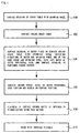
- FIG. 1 is a flow chart showing an exemplary process of a first
embodiment of the method of the invention;
- FIG. 2 is a flow chart showing an exemplary process of a
second embodiment of the method of the invention;
- FIG. 3 is a flow chart showing an exemplary process of a
third embodiment of the method of the invention;
- FIG. 4 is a flow chart showing an exemplary process of a
fourth embodiment of the method of the invention;
- FIG. 5 is an explanatory diagram showing steps of an
exemplary process of a first embodiment of a method of the invention;
- FIG. 6 is an explanatory diagram showing steps of an
exemplary process of a second embodiment of a method of the
invention;
- FIG. 7 is an explanatory diagram showing steps of an
exemplary process of a third embodiment of a method of the
invention;
- FIG. 8 is an explanatory diagram showing steps of an
exemplary process of a fourth embodiment of the method of the
invention;
- FIG. 9 shows patterns of grinding striations produced when a
wafer is surface ground, (a) shows a case of surface grinding of a
wafer in Examples 1 and 2, and (b) a case of surface grinding of a
wafer in Example 3;
- FIG. 10 is an explanatory diagram schematically showing
steps of a prior art surface grinding method for a wafer according to a
process flow thereof, (a) shows surface grinding on a chuck table, (b)
fixing of a wafer on a surface ground chuck table and (c) surface
grinding of a wafer;
- FIG. 11 is an explanatory diagram conceptually showing
variations in grinding removal in a surface grinding operation for a
work by a cup shaped grinding wheel;
- FIG. 12 is an explanatory diagram showing steps of an
exemplary process of a fifth embodiment of a method of the invention;
- FIG. 13 is an explanatory diagram showing steps of an
exemplary process of a sixth embodiment of a method of the
invention;
- FIG. 14 is an explanatory diagram showing steps of an
exemplary process of a seventh embodiment of a method of the
invention; and
- FIG. 15 is an explanatory diagram showing steps of an
exemplary process of an eighth embodiment of a method of the
invention.
-
Best Mode for Carrying Out the Invention
-
Description will be given of embodiments of the invention
below based on FIGs. 1 to 8 and FIGs. 12 to 15 among the
accompanying drawings and it is needless to say that various
modifications or alterations of the embodiments may be possible as
far as not departing from the technical concept of the invention.
-
FIGs. 1 to 4 are flow charts showing exemplary processes of
first to fourth embodiments of a method of the invention. FIGs. 5 to 8
are explanatory diagrams showing steps of the exemplary processes of
the first to fourth embodiments of a method of the invention. FIGs.
12 to 15 are explanatory diagrams showing steps of exemplary
processes of fifth to eighth embodiments of a method of the invention.
-
In the first embodiment of the invention shown in FIG.1, a
chuck table 12 is surface ground by a cup shaped grinding wheel 16 as
shown in FIG. 5(a) (the step 100 of FIG. 1) and the surface ground
chuck table 12 is obtained (the step 102 of FIG.1).
-
A wafer W is fixed on the surface ground chuck table 12 (FIG.
5(b)) and the grinding wheel 16 cuts into the wafer W at the outer
peripheral edge portion and grinds the wafer toward the center
thereof, thus performing surface grinding (the step 104 of FIG. 1 and
FIG. 5(c)).
-
In the first embodiment, a grinding operation to cut into the
wafer W from the outer peripheral edge portion toward the center
thereof is performed by rotating the grinding wheel 16 and the chuck
table 12, that is the wafer W in the same sense of direction in a state
where the rotation axis 14a of the grinding wheel 16 and the rotation
axis 12a of the chuck table 12 form an prescribed inclination of
therebetween. The surface grinding is performed to a removal of the
order of 1 to 50 µm in thickness on one side thereof.
-
The ground surface of the wafer having been surface-ground
in the first embodiment has surface features thereon that there occur
a rise in the outer peripheral edge portion of the wafer and a recess in
the central portion thereof as the section thereof is shown
schematically in FIG. 5(d)) (step 106 of FIG. 1 and FIG. 5(d)).
-
The wafer W surface ground in the first embodiment is
applied in succession with a PACE method to planarize (the step 108
of FIG. 1) to obtain the wafer with improved flatness (the step 110 of
FIG. 1).
-
A difference between the first embodiment and the second
one of the invention shown in FIG. 2 is in that in step 104 of FIG. 1, a
prescribed inclination of shown in FIG. 5(c) formed between the
rotation axis 14a of the grinding wheel 16 and the rotation axis 12a of
the chuck table 12 is replaced with an inclination - in the opposite
direction, and the grinding wheel 16 and the chuck table 12, that is
the wafer W rotate in opposite senses of rotating direction (the step
104a of FIG. 2, FIG. 6(c)) and the rest of the procedures are similar to
each other.
-
A sectional shape of the ground surface of the surface ground
wafer in the second embodiment has a recess similar to FIG. 5(d) (the
step 106 of FIG. 2, FIG. 6(d)). Accordingly, by applying a PACE
method to the wafer with a recess as in the case of the first
embodiment, the wafer W with improved flatness can be obtained (the
step 110 of FIG. 2).
-
FIG. 12 shows steps of an exemplary process of a fifth
embodiment of a method of the invention. In the first and second
embodiments as shown in FIG. 12 (a), surface grinding proceeds
toward the center of the chuck table 12 such that the grinding wheel
16 cuts into the chuck table 12 at the outer peripheral edge thereof
and moves away from the chuck table 12 at the center thereof in the
surface grinding operation for the chuck table 12 (step 100 of FIGs. 1
and 2). Since, in this case, there occur a recess in the vicinity of the
center of the chuck table 12 and a rise in the peripheral edge portion
thereof (FIG. 12(b)), when a wafer W is surface ground using this
chuck table (FIG. 12(c)(d)), there arises an advantage of flatness
improvement in the outer peripheral edge portion and central portion
of the wafer as described previously (FIG. 12(e)).
-
FIG. 15 shows steps of an exemplary process of a eighth
embodiment of a method of the invention. On the contrary, when
surface grinding is performed toward the outer peripheral edge
portion from the central portion on a chuck table such that a grinding
wheel 16 cuts into the chuck table 12 at the center thereof and moves
away from the chuck table 12 at the outer peripheral edge portion
(FIG. 15(a)), there occur a rise in the vicinity of the center of the
chuck table 12 and a sag in the outer peripheral edge portion (FIG.
15(b)); therefore, when a wafer W is surface ground using the chuck
table 12 (FIG. 15(c)(d)), there arises a disadvantage that reduction in
the flatness in the central portion and outer peripheral edge portion
of the wafer W is further exaggerated (FIG. 15(e)). Note that even
this wafer W can be a wafer of having improved flatness when the
wafer W is planarized by applying a PACE method.
-
In the third embodiment of the invention shown in FIG. 3,
the wafer W is fixed on a surface ground chuck table 12 (FIG. 7(b)),
and surface-grinding is performed such that the cup shaped grinding
wheel 16 cuts into the wafer W at the center thereof to grind the
wafer W toward the outer peripheral edge (the step 104b of FIG. 3
and FIG.7(c)).
-
In this third embodiment, surface grinding is performed in a
state that an angle of the rotation axis 12a of the chuck table 12 to
the rotation axis 14a of the grinding wheel 16 is inclined by in the
counterclockwise direction and the grinding wheel 16 and the chuck
table 12, that is the wafer W, rotate in the same rotating direction.
-
The ground surface of the wafer W surface ground in the
third embodiment has a rise produced in the vicinity of the center
thereof and a sag produced in the outer peripheral edge portion
thereof as the section thereof is shown schematically in FIG. 7(d) (the
step 106a of FIG. 3 and FIG. 7(d)).
-
The ground surface of the wafer W surface ground in the
third embodiment is applied in succession with a polishing method,
that is a CMP method, suited for correcting and planarizing the rise
(the step 108a of FIG. 3), thereby enabling achievement of the wafer
with improved flatness (the step 110 of FIG. 3).
-
A difference between the third embodiment shown in FIG. 3
and the fourth one shown in FIG. 4 is only in that in step 104b of FIG.
3, an angle formed between the rotation axis 12a of a rotary shaft of
the chuck table 12 to the rotation axis 14a of the grinding wheel 16 is
adjusted so as to be an inclination in the direction opposite to the
prescribed inclination shown in FIG. 7(c) as well as the grinding
wheel 16 and the chuck table 12, that is the wafer W rotate in
opposite rotating directions (the step 104c of FIG.4 and FIG. 8(c)) and
both embodiments are similar to each other in the rest of the
procedures.
-
The wafer W surface ground in the fourth embodiment has a
rise in the vicinity of the center thereof similar to the case of FIG.
7(d)(the step 106a of FIG. 4 and FIG. 8(d)).
-
The wafer W surface ground in the fourth embodiment is also
polished by CMP in the similar manner to the third embodiment (the
step 108a of FIG. 4), thereby enabling achievement of the wafer with
improved flatness (the step 110 of FIG. 4).
-
FIG. 14 shows steps of an exemplary process of a seventh
embodiment of a method of the invention. In the third and fourth
embodiments as shown in FIG. 14(a), the chuck table 12 is ground and
finished toward the outer peripheral edge thereof from the center
thereof such that the grinding wheel 16 cuts into the chuck table 12
at the center thereof and moves away from the chuck table 12 at the
outer peripheral edge portion thereof in a surface grinding operation
of the chuck table 12 (the step 100 of FIGs. 3 and 4), and on the thus
ground chuck table 12, there occur a rise in the vicinity of the center
thereof and a sag in the outer peripheral edge portion thereof (FIG.
14(b)); therefore, when a wafer W is surface ground using this chuck
table 12 (FIG. 14(c)(d)), an advantage is enjoyed in that a rise in the
vicinity of the center of the ground wafer and a sag in the outer
peripheral edge portion thereof are improved as described previously
(FIG. 14(e)).
-
FIG. 13 shows steps of an exemplary process of a sixth
embodiment of a method of the invention. On the contrary, when the
chuck table 12 is ground and finished toward the center thereof from
the outer peripheral edge thereof such that the grinding wheel 16 cuts
into the chuck table 12 at the outer peripheral edge portion thereof
and moved away from the chuck table 12 at the center thereof (FIG.
13(a)), on the chuck table 12 there occur a recess in the vicinity of the
center thereof and a rise in the outer peripheral edge portion thereof
(FIG. 13(b)); therefore, when the wafer W is surface ground using this
chuck table 12 (FIG. 13(c)(d)), there arises a disadvantage that
reduction in the flatness in the vicinity of the center of the wafer W
and in the outer peripheral edge portion is further exaggerated (FIG.
13(e)). Note that by applying CMP to this wafer W to polish as well,
the wafer with improved flatness can be achieved.
-
Note again that when the chuck table 12 is in a state that the
table 12 is suited for use in surface grinding of a wafer W by having
been surface ground once, there may be no need for surface grinding
of the chuck table 12 each time a wafer W is surface ground; therefore,
the steps 100 and 102 are omitted in some cases.
-
While description will be given of the invention in a concrete
manner below with reference to examples, needless to say that
descriptions of the examples are shown by way of exemplification but
should not be construed as any limitation on the invention. Note
that while etched silicon wafers each of 300 mm in diameter were
employed as specimen wafers in the following examples and
comparative examples, it has been confirmed that results of the
examples and comparative examples apply to etched silicon wafers
each of 200 mm in diameter in a similar way.
(Example 1)
-
Wafers W were surface ground according to the method
shown in FIGs. 1 and 5. Grinding conditions this time are as follows.
A chuck table was used of a type of a circular cone.
- Grinding wheel: a resinoid bonded cup shaped grinding wheel using #
2000 diamond abrasive powder,
- Peripheral velocity of the grinding wheel: 60 m/sec,
- Peripheral velocity of the wafer in rotation: 0.06 to 0.5 m/sec at the
outer peripheral edge thereof,
- Rotating direction of the grinding wheel and the wafer: the same
direction,
- Feed rate of the grinding wheel: 0.1 to 0.3 µm/sec.
-
-
In this method, the cup shaped grinding wheel 16 and each
wafer W are put into contact with each other at the outer peripheral
edge and the cup shaped grinding wheel cuts into the wafer W thereat.
The grinding wheel 16 thus cut in is moved, while rotating, toward
the center of the wafer and the cutting is completed at the center and
moves away from the wafer thereat. Removals of the ground
surfaces of the wafers W were in the range of 10 to 20 µm in thickness.
Grinding striations of each wafer W surface ground according to the
method of FIG. 5 were as shown in FIG. 9(a).
-
A flatness of each of the wafers W surface ground was
measured using a measuring instrument of a capacitive sensing type
(made by ADE Co., Model: Galaxy AFS 300) and as a result, a
thickness variation across a wafer surface was 0.5 µm or less
excluding the central portion and outer peripheral edge portion.
Measured values of the recess were observed at 0.5 µm as the
maximum depth in a circular area of 5 mm in radius from the center,
while measured values of the rise were observed at 0.3 µm as the
maximum height in an annular area of 5 mm in width inward from
the outer peripheral edge. The wafers W were planarized with a
PACE method (Plasma Assisted Chemical Etching: made by IPEC
Precision, Inc., Model: PWS 300). The ground surface other than a
recess in the central portion of each wafer W was removed by means
of the PACE method by about 1 µm and a rise in the outer peripheral
edge portion was also effectively removed, with the result that
flatness of the wafer was globally improved and values of flatness
SBIR (Site Back-side Ideal Range, which is the same definition as
LTV = Local Thickness Variation) in the vicinity of the center of each
of the wafers W were in the range of 0.10 µm or less, which range was
equal to that in a region other than an area in the vicinity of the
center of each wafer. Note that the measurements of SBIR were
performed in a cell size of 25 mm x 25mm with edge exclusion of 3mm
for each measurement including other examples and comparative
examples.
(Comparative Example 1)
-
Wafers W were surface grounded in the procedure similar to
that of Example 1. There were observed a recess and a rise in the
vicinity of the center and in the outer peripheral edge portion,
respectively, of each wafer W. The wafers W were CMP polished by
a stock removal of about 5 µm using a polishing cloth of a hard
urethane type or a urethane-impregnated type. In this polishing
step, a recess in the vicinity of the center of each wafer W was
polished to the same extent as in the other area of the wafer;
therefore, no correction was achieved on the recess after the polishing.
As a result, a flatness in an area other than in the vicinity of the
center of each wafer was 0.10 µm or less in SBIR, while a flatness in
the vicinity of the center thereof fell in the range of 0.25 to 0.50 µm
on each wafer.
(Example 2)
-
Wafers were surface ground according to the method shown
in FIGs. 4 and 8. Conditions for grinding are the same as in Example
1 with the exception that rotating directions of a grinding wheel and a
wafer are opposite from each other. A chuck table was almost in the
shape of a circular cone. In this method, a cup shaped grinding
wheel 16 and a wafer W are put into contact with each other at the
center of the wafer and the grinding wheel 16 cuts into the wafer
thereat. The grinding wheel completed the cutting at the outer
peripheral edge of each wafer and moves away from the wafer there.
The ground surface of each wafer was ground off by 10 to 20 µm in
thickness. Grinding striations on each wafer surface ground
according to a method of FIGS. 4 and 8 were the same as shown in Fig.
9(a).
-
Flatness of each wafer W surface ground was measured and
as a result, a thickness variation across each wafer surface was 0.5
µm or less except for the central portion and outer peripheral edge
portion of the wafer. There were recognized on each wafer W a rise
of 0.5 µm in height at the maximum in a circular area of a radius of
about 5 mm from the center, and a sag of 0.3 µm in depth at the
maximum in an annular area of 5 mm in width inward from the outer
_peripheral edge. Each of the wafers surface ground was CMP
polished using a polishing cloth of a hard urethane type or a urethane
impregnated type by a stock removal of about 5 µm and flatness was
measured on each wafer, with the result that values of flatness SBIR
in the vicinity of the center and the outer peripheral portion of each
wafer were in the range of 0.10 µm or less, which range was almost
equal to that in an area other than the vicinity of the center and the
outer peripheral portion of each wafer.
(Example 3)
-
As shown in FIG. 7, wafers W were surface ground such that
the cup shaped grinding wheel 6 cuts into each wafer at the central
portion thereof and moves away from the wafer at the outer
peripheral edge portion thereof in conditions that the rotating
direction of a cup shaped grinding wheel 16 was the same as in the
case of FIG. 5, while an inclination of the rotation axis of the chuck
table 12 to the rotation axis of the grinding wheel 16 is altered to the
opposite directions from that in the case of FIG. 5. A chuck table in
use was almost in the shape of a circular cone. The wafers W were
surface ground according to the method shown in FIGs. 3 and 7 and
as a result, there was recognized on each wafer a characteristic rise
in the vicinity of the center thereof (FIG. 7(d)) in the similar manner
to the wafers W in Example 2 (according to the method of FIGs. 4 and
8). Grinding striations on each wafer W surface ground this time
were as shown in FIG. 9(b). The wafers W surface ground in such a
way were CMP polished by a stock removal of about 5 µm similar to
Example 2 and as a result, each wafer achieved good flatness.
(Example 4)
-
A chuck table 12 for use in fixing a semiconductor wafer
thereon was surface ground according to the method shown in FIG.
12(a) using the cup shaped grinding
wheel 16. In this method, the
cup shaped grinding
wheel 16 is put into contact with the outer
peripheral edge of the chuck table 12 and cuts into the chuck table 12
thereat. The grinding wheel cut in is moved while rotating toward
the center of the chuck table 12, the cutting is completed at the center
thereof and the grinding wheel moves away from the chuck table 12
thereat.
Conditions for the grinding at this time were as follows.
- Grinding wheel: a metal bonded cup shaped grinding wheel using #
600 diamond abrasive powder,
- Peripheral velocity of the grinding wheel: 50 m/sec,
- Speed of rotation of the chuck table: 0.6 m/sec at the outer peripheral
edge,
- Feed rate of the grinding wheel: 0.3 µm/sec,
- Rotating direction of the grinding wheel and the chuck table: the
same direction.
-
-
In this surface grinding, the chuck table 12 was finished so
as to be in the shape of a slightly inclined circular cone with the
center thereof as a vertex of the circular cone. The chuck table 12
was surface ground according to the method in FIG. 12(a) and on the
conical surface, there were recognized a rise of 0.2 µm in height in an
annular region of 5 mm in width inward from the outer peripheral
edge of the chuck table 12 and a recess of about 0.5 µm in depth in a
circular area with a radius of about 5 mm from the center of the chuck
table 12 and in the vicinity of the vertex of the circular cone (FIG.
12(b)).
-
Each wafer was vacuum chucked on the chuck table (FIG.
12(c)) and the cup shaped grinding wheel 16 was put into contact with
the outer peripheral edge and cuts into the wafer thereat; then, the
wafer was surface ground in the conditions similar to those in
Example 1 (FIG. 12(d)). The grinding wheel cut in was moved while
rotating toward the center of the wafer, completed the cutting at the
center of the wafer and then moves away from the wafer thereat. In
this surface grinding, a resinoid bonded cup shaped grinding wheel
was used as the cup shaped grinding wheel 16. All the wafers were
surface grounded according to this method and as a result, extremely
good flatness of 0.2 µm or less in GBIR (Global Back-side Ideal Range,
which is the same definition as TTV = Total Thickness Variation) was
obtained on each wafer (FIG. 12(e)).
(Example 5)
-
A chuck table surface ground (FIG. 13(a)) similar to Example
4 was obtained (FIG. 13(b)). Each wafer was vacuum chucked on
this chuck table (FIG. 13(c)) and ground in the conditions similar to
those in Example 4 except that rotating directions of a grinding wheel
16 and the wafer were opposite from each other, wherein the cup
shaped grinding wheel 16 was put into contact with the center of the
wafer and cuts into the wafer thereat (FIG. 13(d)). The grinding
wheel cut in was moved while rotating toward the outer peripheral
edge of the wafer to complete the cutting thereat and moved away
from the wafer there. In this surface grinding, a resinoid bonded cup
shaped grinding wheel was used as the cup shaped grinding wheel 16.
All the wafers were surface ground and as a result, on each wafer,
there occurred an exaggerated rise as high as about 0.8 µm in height
in the vicinity of the center of the wafer and an exaggerated sag in an
annular area of about 5 mm in width inward from the outer
peripheral edge thereof, a depth of which sag amounted to 0.6 µm.
The wafers were CMP polished similar to Example 2 and good flatness
was achieved on each of them.
(Example 6)
-
A chuck table 12 on which a semiconductor wafer is fixed was
surface ground using a cup shaped grinding wheel 16 according to the
method shown in FIG. 14(a). Grinding conditions at this time were
similar to those in Example 4 except that rotating directions of the
grinding wheel and the chuck table were opposite from each other.
In this method, the cup shaped grinding wheel 16 was put into
contact with the chuck table 12 in the vicinity of the center thereof
and cuts into the chuck table thereat. The grinding wheel cut in is
moved while rotating toward the outer peripheral edge of the chuck
table to complete the cutting at the outer peripheral edge thereof and
moved away from the chuck table thereat. In this surface grinding,
a metal bonded cup shaped grinding wheel was used as the cup
shaped grinding wheel 16 and the chuck table 12 was shaped as a
circular cone whose surface is inclined slightly from its original
surface of the chuck table, the vertex of the cone being the center of
the chuck table surface. On the chuck table 12 surface ground
according to the method shown in FIG. 14(a), there occurred sag of
about 0.2 µm in depth extending from the conical surface in an annual
area of 5 mm in width inward from the outer peripheral edge of the
chuck table 12 and a rise of about 0.5 µm in height in a circular area
of about 5 mm in radius from the center thereof, the circular area
being the central portion of the chuck table 12 in the vicinity of the
vertex of the circular cone (FIG. 14(b)).
-
Each wafer was vacuum chucked on the chuck table (FIG.
14(c)) and ground in the conditions similar to those in Example 1
except that rotating directions of the grinding wheel and the wafer
are opposite from each other, wherein the cup shaped grinding wheel
16 cuts into the wafer at the center thereof (FIG. 14(d)). The
grinding wheel cut in was moved while rotating toward the outer
peripheral edge of the wafer to complete the cutting at the outer
peripheral edge and moved away from the wafer thereat. In this
surface grinding, a resinoid bonded cup shaped grinding wheel was
used as the cup shaped grinding wheel 16. All the wafers were
surface ground and as a result, extremely good flatness equal to or
less than 0.2 µm or less in GBIR (the same as TTV) was able to be
obtained on each wafer (FIG. 14(e)).
(Example 7)
-
A chuck table surface-ground (FIG. 15(a)) in the procedure
similar to that of Example 6 was obtained (FIG. 15(b)). Each wafer
was vacuum chucked on this chuck table (FIG. 15(c)) and ground in
the conditions similar to those of Example 6 except that rotating
directions of the grinding wheel and the wafer are of the same sense,
wherein the cup shaped grinding wheel 16 was put into contact with
the outer peripheral edge of the wafer and cut into the wafer thereat
(FIG. 15(d)). The grinding wheel cut in was moved while rotating
toward the center of the wafer to complete the cutting thereat and
move away from the wafer thereat. In this surface grinding, a
resinoid bonded cup shaped grinding wheel was used as the cup
shaped grinding wheel 16. All the wafers were surface ground
according to this method and as a result, on each wafer, there
occurred an exaggerated recess (about 0.8 µm in depth) in the central
portion thereof and a rise having an exaggerated profile of an upward
slope with the top at the outer peripheral edge, as high as about 0.6
µm in height in the vicinity of the outer peripheral edge (FIG. 15(e)).
Each wafer was planarized by means of the PACE method similar to
that of Example 1, enabling achievement of good flatness on the
wafer.
(Example 8)
-
Each of surface ground wafers was CMP polished and
polishing was performed such that a sense of rotating direction of the
wafer was in a direction toward which grinding striations on the
wafer are convex. A polishing cloth of a hard urethane type or a
urethane impregnated type was used in the CMP. In this case, a
resistance to polishing became smaller and vibrations of the wafer
during polishing were less, with the result that a lifetime of the
polishing cloth was longer than when etched wafers without surface
grinding, produced in the prior art were polished by about 20 %.
(Comparative Example 3)
-
In a step where each surface ground wafer was CMP polished,
the wafer was polished such that rotating direction of the wafer was
in a direction toward which grinding striations on the wafer are
concave. A polishing cloth of a hard urethane type or a urethane
impregnated type was used. In this case, a resistance to polishing
became larger and vibrations of the wafer during polishing were more,
with the result that a lifetime of the polishing cloth was shorter
compared with Example 8 by as large as 30 to 50 %.
Capability of Exploitation in Industry
-
As described above, according to the invention, abnormalities
in flatness occurring in the vicinity of the center and in the peripheral
edge portion of a ground surface of a wafer are restricted at the
possible lowest level and a planarization or polishing method suited
for correcting such abnormalities in flatness is used to correct and
planarize the wafer and thereby a large effect can be achieved that
semiconductor wafers each with high flatness are manufactured with
good efficiency.