EP1137187A2 - Phase locked loop - Google Patents
Phase locked loop Download PDFInfo
- Publication number
- EP1137187A2 EP1137187A2 EP00310711A EP00310711A EP1137187A2 EP 1137187 A2 EP1137187 A2 EP 1137187A2 EP 00310711 A EP00310711 A EP 00310711A EP 00310711 A EP00310711 A EP 00310711A EP 1137187 A2 EP1137187 A2 EP 1137187A2
- Authority
- EP
- European Patent Office
- Prior art keywords
- equation
- phase
- vco
- circuit
- loop
- Prior art date
- Legal status (The legal status is an assumption and is not a legal conclusion. Google has not performed a legal analysis and makes no representation as to the accuracy of the status listed.)
- Withdrawn
Links
Images







Classifications
-
- H—ELECTRICITY
- H03—ELECTRONIC CIRCUITRY
- H03L—AUTOMATIC CONTROL, STARTING, SYNCHRONISATION OR STABILISATION OF GENERATORS OF ELECTRONIC OSCILLATIONS OR PULSES
- H03L7/00—Automatic control of frequency or phase; Synchronisation
- H03L7/06—Automatic control of frequency or phase; Synchronisation using a reference signal applied to a frequency- or phase-locked loop
- H03L7/08—Details of the phase-locked loop
- H03L7/099—Details of the phase-locked loop concerning mainly the controlled oscillator of the loop
- H03L7/0991—Details of the phase-locked loop concerning mainly the controlled oscillator of the loop the oscillator being a digital oscillator, e.g. composed of a fixed oscillator followed by a variable frequency divider
- H03L7/0994—Details of the phase-locked loop concerning mainly the controlled oscillator of the loop the oscillator being a digital oscillator, e.g. composed of a fixed oscillator followed by a variable frequency divider comprising an accumulator
-
- H—ELECTRICITY
- H03—ELECTRONIC CIRCUITRY
- H03L—AUTOMATIC CONTROL, STARTING, SYNCHRONISATION OR STABILISATION OF GENERATORS OF ELECTRONIC OSCILLATIONS OR PULSES
- H03L7/00—Automatic control of frequency or phase; Synchronisation
- H03L7/06—Automatic control of frequency or phase; Synchronisation using a reference signal applied to a frequency- or phase-locked loop
-
- H—ELECTRICITY
- H03—ELECTRONIC CIRCUITRY
- H03L—AUTOMATIC CONTROL, STARTING, SYNCHRONISATION OR STABILISATION OF GENERATORS OF ELECTRONIC OSCILLATIONS OR PULSES
- H03L7/00—Automatic control of frequency or phase; Synchronisation
- H03L7/06—Automatic control of frequency or phase; Synchronisation using a reference signal applied to a frequency- or phase-locked loop
- H03L7/08—Details of the phase-locked loop
-
- H—ELECTRICITY
- H03—ELECTRONIC CIRCUITRY
- H03L—AUTOMATIC CONTROL, STARTING, SYNCHRONISATION OR STABILISATION OF GENERATORS OF ELECTRONIC OSCILLATIONS OR PULSES
- H03L7/00—Automatic control of frequency or phase; Synchronisation
- H03L7/06—Automatic control of frequency or phase; Synchronisation using a reference signal applied to a frequency- or phase-locked loop
- H03L7/08—Details of the phase-locked loop
- H03L7/085—Details of the phase-locked loop concerning mainly the frequency- or phase-detection arrangement including the filtering or amplification of its output signal
- H03L7/093—Details of the phase-locked loop concerning mainly the frequency- or phase-detection arrangement including the filtering or amplification of its output signal using special filtering or amplification characteristics in the loop
Definitions
- the present invention relates to phase locked loop topology including and, more particularly, but not exclusively, the phase locked loop technology for compensating for the effects of loop latency in a read channel.
- phase locked loops for hard disk drives (HDD) data recovery has been used by implementing decision directed algorithms to adjust the frequency and phase of the recovered clock in order to optimize the sampling instants (timing instants) of the received signals.
- decision directed algorithms which, by their very nature, depend on a reliable estimate (decision) of the current sample, have grown in complexity as the read channel signal processing has moved to higher partial response polynomials.
- One way of obtaining reliable phase error estimates relies on obtaining decision (binning) information from the Viterbi detector. Because of the complexity associated with this block, these topologies are characterized by latencies, usually symbolized by the term mD, which can be easily in excess of 20 clock cycles.
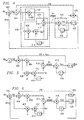
- Figure 1 illustrates one such circuit.
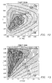
- FIGS. 2 and 3 show how one such region varies as the latency increases from one clock cycle (ideal) to 19 clock cycles (representative of a medium latency digital PLL).
- the loop gain reduction needs to be larger. Under most circumstances, this causes poor performance and sluggish response within the PLL.
- Loop latency also has a significant impact on the design of the time base generator, which is a circuit that generates the reference clock for the PLL.
- the present invention provides a circuit that eliminates or at least reduces the latency associated with external delays.
- a feedback loop is provided to eliminate or reduce these delays.
- An embodiment of the present invention provides a substantially zero steady state error in the presence of offsets between the frequency of the input signal and the frequency of the reference clock.
- Figures 19 and 20 show a side and top view, respectively, of the disk drive system designated by the general reference 100 within an enclosure 110.
- the disk drive system 100 includes a plurality of stacked magnetic recording disks 112 mounted to a spindle 114.
- the disks 112 may be conventional particulate or thin film recording disk or, in other embodiments, they may be liquid-bearing disks.
- the spindle 114 is attached to a spindle motor 116 which rotates the spindle 114 and disks 112.
- a chassis 120 is connected to the enclosure 110, providing stable mechanical support for the disk drive system.
- the spindle motor 116 and the actuator shaft 130 are attached to the chassis 120.
- a hub assembly 132 rotates about the actuator shaft 130 and supports a plurality of actuator arms 134.
- the stack of actuator arms 134 is sometimes referred to as a "comb.”
- a rotary voice coil motor 140 is attached to chassis 120 and to a rear portion of the actuator arms 134.
- a plurality of head suspension assemblies 150 are attached to the actuator arms 134.
- a plurality of inductive transducer heads 152 are attached respectively to the suspension assemblies 150, each head 152 including at least one inductive write element.
- each head 152 may also include an inductive read element or a MR (magneto-resistive) read element.
- the heads 152 are positioned proximate to the disks 112 by the suspension assemblies 150 so that during operation, the heads are in electromagnetic communication with the disks 112.
- the rotary voice coil motor 140 rotates the actuator arms 134 about the actuator shaft 130 in order to move the head suspension assemblies 150 to the desired radial position on disks 112.
- a controller unit 160 provides overall control to the disk drive system 100, including rotation control of the disks 112 and position control of the heads 152.
- the controller unit 160 typically includes (not shown) a central processing unit (CPU), a memory unit and other digital circuitry, although it should be apparent that these aspects could also be enabled as hardware logic by one skilled in the computer arts.
- Controller unit 160 is connected to the actuator control/drive unit 166 which is in turn connected to the rotary voice coil motor 140.
- a host system 180 typically a computer system or personal computer (PC), is connected to the controller unit 160. The host system 180 may send digital data to the controller unit 160 to be stored on the disks, or it may request that digital data at a specified location be read from the disks 112 and sent back to the host system 180.
- a read/write channel 190 is coupled to receive and condition read and write signals generated by the controller unit 160 and communicate them to an arm electronics (AE) unit shown generally at 192 through a cut-away portion of the voice coil motor 140.
- the AE unit 192 includes a printed circuit board 193, or a flexible carrier, mounted on the actuator arms 134 or in close proximity thereto, and an AE module 194 mounted on the printed circuit board 193 or carrier that comprises circuitry preferably implemented in an integrated circuit (IC) chip including read drivers, write drivers, and associated control circuitry.
- the AE module 194 is coupled via connections in the printed circuit board to the read/write channel 190 and also to each read head and each write head in the plurality of heads 152.
- the read/write channel 190 includes the PLL circuit of the present invention.
- Equation (3) implies that the PLL loop would process the same correction twice, once at time index n-1 and once at time index n-m-2. Since this is not desirable, it is more desirable to eliminate the ⁇ vco n-m -2 term. This operation can be accomplished by redifining ⁇ as illustrated in Equation (4).
- ⁇ n is input to adder circuit 402. Additionally, ⁇ vco is input to the negative input of adder circuit 402.
- the output signal ⁇ of adder circuit 402 is input to adder circuit 404.
- signal ⁇ is input to adder circuit 404.
- Output from adder circuit 404 is the signal ⁇ which is input both to multiplier 406 and multiplier 408.
- the multiplier 406 amplifies ⁇ by ⁇ and is output to adder circuit 410.
- the multiplier circuit 408 multiplies ⁇ by ⁇ and outputs ⁇ to the adder circuit 412.
- the output of adder circuit 412 is delayed by delay circuit 414 and input to adder circuit 412.
- the output of adder circuit 412 is additionally input to adder circuit 410.
- the output of adder circuit 410 is signal phUpdate n-1 and input to adder circuit 416.
- the output of adder circuit 416 is ⁇ vco which is input to delay circuit 418.
- the output of delay circuit 418 is input to adder circuit 416.
- the output of adder circuit 416 ⁇ vco is input both to adder circuit 420 and delay circuit 422.
- the delay circuit 422 represents the delay associated with the sampling (A/D), equalization (FIR) and phase detector circuits.
- the output of delay circuit 422 is input to adder circuit 420 and also as ⁇ vco to adder circuit 402.
- the output of adder circuit 420 ⁇ is input to adder circuit 404.
- the proportional branch 432 includes multiplier 406, and the integral branch 434 includes multiplier 408, adder 412 and delay 414. Adder 412 in conjunction with delay 414 is also an integral accumulator.
- the Vco accumulator 436 includes adder 416 and delay 418.
- the Pll filter 430 includes the porportional branch 432 and the integral branch 434.
- ⁇ n the delay compensation feedback
- the delay compensation gain ⁇ is a parameter which allows to turn on and turn off the effects of the delay compensating network.
- ⁇ vco is the delayed version of ⁇ vco
- Equation (6) Equation (6): where m is the portion of the overall loop latency due to the sampling network (e.g. AID), equalization circuits (e.g. FIR) and phase detector (inclusive of Viterbi processing latency) of the read channel 190.
- ⁇ vco is the phase of the sampling clock.
- Equation (7) The fundamental Vco update equation is shown in Equation (7):
- Equation (9) For a traditional PI filter, we have Equation (9):
- Equation (12) From Equations (5) and (10) we obtain Equation (12):
- Equation (13) Taking the z-transform of (12), we obtain an open loop transfer function in Equation (13):
- the open loop transfer functions contain a z -m factor associated with loop latency.
- Equation (14) can be manipulated to yield Equation (15):
- Equation (16) Taking the z-transform of (15), the following closed loop transfer function in Equation (16) is obtained:
- Equation (18) Equation (18):
- Equation (19) Taking the z-transform of Equation (18), we can obtain the following closed loop transfer function, expressed by Equation (19):
- Equation (23) The steady state errors to some common inputs, for example the steady state error to a phase step ⁇ , is given by Equation (23):
- Equation (24) The steady state error to a frequency step w 0 is given by Equation (24):
- Equation (24) leads us to a limitation of the present scheme, as shown in Figure 4, that the steady state error due to a frequency step is non-zero and depends on the latency of the loop m.
- Equation (25) indicates that the feedback loop as shown in Figure 5 is aligning the current phase of the Vco to the phase of the input signal m clock cycles earlier. Equation (24) is then the result.
- Equation (26) has to go to zero faster than (z-1) for the limit in Equation (24) to yield zero.
- the coefficient of the integral gain ⁇ in the numerator must be either 0 or contain a (z-1) term. When either condition is met, the system should be able to track a frequency step with zero steady state error.
- Equation (27) ⁇ ( ⁇ n-m-3 - ⁇ n-m-4 ) + ⁇ ⁇ err n-m-5
- Equation (27) reflects the fact that the integral path is being driven by ⁇ err (scheme A).
- Equation (27a) yields the open loop transfer function in the z-domain, expressed as Equation (28):
- Equation (27) in view of Equation (11) is transformed to Equation (29):
- Equation (30) The closed loop transfer function in the z-domain is illustrated in Equation (30).
- Equation (30) If we compare Equation (30) to the one obtained for the topology of Figure 4, Equation (19), the term z -m can no longer be factored out. The consequence of this is that the loop latency will be only partially compensated, but the system will deal with the frequency uncertainties as discussed above.
- Equation (31) The error gain is illustrated in Equation (31):
- Equation (31) is no longer dependent on ⁇ in the numerator.
- Equation (32) The steady state error in response to a phase step is defined by Equation (32):
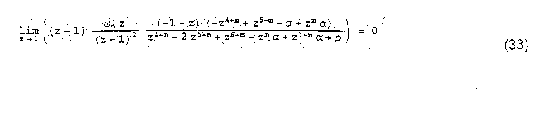
- Equation (33) The steady state error to a frequency step ⁇ 0 is Equation (33):
- Delay compensation approach includes removing the phase correction due to the vco phase update of time index n-m-2 as illustrated in Equation (4) and replacing it with the correction due to the phase update of time index n-2.
- the cancellation may not be complete.
- m is the sum of two terms
- a term associated with an analog delay and a term associated with a digital delay The first term will, in general, pose a problem because it is not a well-defined multiple of the clock period due to its dependency on process and operating conditions.
- Equation (36) (z -m ( ⁇ (z -5 - z -6 ) + ⁇ z -6 )) / (1 - 2 z -1 + z -2 + ⁇ ((z -m-5 + z -5- ⁇ - z -m-5- ⁇ ) - (z -m-6 + z -6- ⁇ - z -m-6- ⁇ )) + ⁇ z -m-6 )
- the error gain becomes Equation (37): ((-1 + z) (-z 4+m+ ⁇ + z 5+m+ ⁇ - ⁇ + z m ⁇ )) / (z 4+m+ ⁇ - 2 z 5+m+ ⁇ + z 6+m+ ⁇ + ⁇ - z ⁇ - z m ⁇ + z 1+m ⁇ - z ⁇ ⁇ + z 1+ ⁇ ⁇ + z ⁇ ⁇ )
- Equation (38) The steady state error in response to a phase step is Equation (38): while the steady state error to a frequency step ⁇ 0 is Equation (39):
- Equations 41, 42 and 43 apply:
- Equations (44), (45) and (46) in the z-domain allow Equations (44), (45) and (46) in the z-domain:
- Equation 49 The open loop gain is shown in Equation 49.
- Equation (51) The steady state error in response to a phase step is shown in Equation (51): while the steady state error to a frequency step is Equation (52): which vanishes for m ⁇ ⁇ .
- Equation (53) The steady state error to a frequency ramp of slope 1 / 2 is Equation (53):
- Figure 9 shows a modified version of the block diagram in Figure 1.
- Figure 9 illustrates a split latency m in two terms j and k, delay backs 902 and 904.
- the first one, delay back 904 represents the delay from the time the input signal is sampled to the time the corresponding phase error is computed and outputted from the phase detector.
- the second term k, delay back 902 represents the time that elapses between a Vco phase update and the time the sampling position moves accordingly.
- Figure 10 shows the corresponding delay compensated version (scheme A).
- An embodiment of the present invention increases the system stability region. Because the stability region is significantly larger than in the uncompensated case, the tracking optimization is improved.
- This contour plot has been generated by compiling, for a given ⁇ and ⁇ , the poles of Equation (16) and reporting the magnitude of the pole further from the origin.
- ⁇ 1 those settings for which such value is ⁇ 1 will correspond to stable operating points.
- the ranges of the loop parameters ⁇ (x-axis) and ⁇ (y-axis) have been adjusted to maximize the operating region, which is the region in which the system is stable.
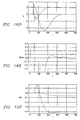
- Figures 13 and 14 show the stability region when using the topologies presented in Figures 6 and 7. When compared to Figure 12, it can be concluded that the stability region has increased by a factor of 20.
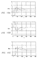
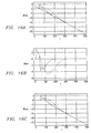
- the loop bandwidth is no longer limited by the loop latency and can be optimized on the basis of input noise and reference clock noise characteristics.
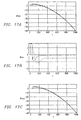
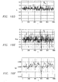
- the compensated topology presents a clear advantage, as illustrated in Figure 18.
Landscapes
- Stabilization Of Oscillater, Synchronisation, Frequency Synthesizers (AREA)
- Signal Processing For Digital Recording And Reproducing (AREA)
Abstract
Description
PLL circuit and is based upon the concept that every time the PLL Vco phase is updated, it obeys the following equation (Figure 1):











The compensated system, γ = 1 is now discussed.
























Claims (2)
- A phase locked loop circuit for reducing loop latency, comprising:an input circuit for inputting a phase signal corresponding to phase changes and an actual phase signal corresponding to actual phase sampling of a sampling clock;a filter circuit for connecting said phase signal and said actual phase signal to a phase update signal; anda feedback circuit to reduce said loop latency by feeding back to said filter circuit a portion of said phase update signal.
- A phase locked loop circuit according to claim 1, for eliminating loop latency, wherein said feedback circuit is configured to eliminate said loop latency.
Applications Claiming Priority (2)
| Application Number | Priority Date | Filing Date | Title |
|---|---|---|---|
| US16890399P | 1999-12-03 | 1999-12-03 | |
| US168903P | 1999-12-03 |
Publications (2)
| Publication Number | Publication Date |
|---|---|
| EP1137187A2 true EP1137187A2 (en) | 2001-09-26 |
| EP1137187A3 EP1137187A3 (en) | 2004-04-21 |
Family
ID=22613430
Family Applications (1)
| Application Number | Title | Priority Date | Filing Date |
|---|---|---|---|
| EP00310711A Withdrawn EP1137187A3 (en) | 1999-12-03 | 2000-12-01 | Phase locked loop |
Country Status (5)
| Country | Link |
|---|---|
| EP (1) | EP1137187A3 (en) |
| JP (1) | JP2001202721A (en) |
| KR (1) | KR20010067376A (en) |
| SG (1) | SG94352A1 (en) |
| TW (1) | TW498620B (en) |
Cited By (1)
| Publication number | Priority date | Publication date | Assignee | Title |
|---|---|---|---|---|
| US9559836B1 (en) | 2015-08-31 | 2017-01-31 | Renesas Electronics Corporation | Clock data recovery circuit |
Families Citing this family (1)
| Publication number | Priority date | Publication date | Assignee | Title |
|---|---|---|---|---|
| JP5251759B2 (en) * | 2009-07-01 | 2013-07-31 | ソニー株式会社 | PLL circuit |
Family Cites Families (6)
| Publication number | Priority date | Publication date | Assignee | Title |
|---|---|---|---|---|
| JP3241079B2 (en) * | 1992-02-24 | 2001-12-25 | 株式会社日立製作所 | Digital phase locked loop |
| US5428317A (en) * | 1994-09-06 | 1995-06-27 | Motorola, Inc. | Phase locked loop with low power feedback path and method of operation |
| EP0718963A1 (en) * | 1994-12-22 | 1996-06-26 | AT&T Corp. | Method and apparatus for broadband frequency modulation of a phase-locked frequency synthesizer |
| JP3639000B2 (en) * | 1995-06-13 | 2005-04-13 | 富士通株式会社 | Phase matching device and delay control circuit |
| US5859550A (en) * | 1995-12-19 | 1999-01-12 | Cisco Technology, Inc. | Network switching system including a zero-delay output buffer |
| JPH1174787A (en) * | 1997-08-27 | 1999-03-16 | Sony Corp | Phase locked loop circuit |
-
2000
- 2000-11-29 SG SG200007081A patent/SG94352A1/en unknown
- 2000-12-01 EP EP00310711A patent/EP1137187A3/en not_active Withdrawn
- 2000-12-02 KR KR1020000072666A patent/KR20010067376A/en not_active Withdrawn
- 2000-12-04 JP JP2000369087A patent/JP2001202721A/en not_active Abandoned
-
2001
- 2001-02-12 TW TW089125690A patent/TW498620B/en not_active IP Right Cessation
Cited By (1)
| Publication number | Priority date | Publication date | Assignee | Title |
|---|---|---|---|---|
| US9559836B1 (en) | 2015-08-31 | 2017-01-31 | Renesas Electronics Corporation | Clock data recovery circuit |
Also Published As
| Publication number | Publication date |
|---|---|
| TW498620B (en) | 2002-08-11 |
| SG94352A1 (en) | 2003-02-18 |
| EP1137187A3 (en) | 2004-04-21 |
| KR20010067376A (en) | 2001-07-12 |
| JP2001202721A (en) | 2001-07-27 |
Similar Documents
| Publication | Publication Date | Title |
|---|---|---|
| US6236343B1 (en) | Loop latency compensated PLL filter | |
| US5847890A (en) | Magnetic disk apparatus and a thermal asperity compensation method of the same | |
| CN101930750B (en) | Systems and methods for hard disk drive data storage | |
| KR100518553B1 (en) | Apparatus and method for suppressing mechanical resonance using an adaptive notch filter | |
| JP2003281831A (en) | Information recording / reproducing apparatus, signal decoding circuit and method | |
| US6950274B2 (en) | Disk storage apparatus and disk storage apparatus control method | |
| US8406351B1 (en) | Method and device to compensate for baseline wander | |
| JP2011030204A (en) | System and method for two tier sampling correction in data processing circuit | |
| KR100260549B1 (en) | Read channel circuit for optical disc reproduction device | |
| JP4480191B2 (en) | Phase locked loop system | |
| JP3129156B2 (en) | Phase detection method and its implementation device | |
| US8773808B2 (en) | Magnetic disk device and head-position control method | |
| JP4016143B2 (en) | Reproduction signal waveform processing apparatus and reproduction signal waveform processing method | |
| JPH08147887A (en) | Decoding circuit and reproducing device | |
| US20060181975A1 (en) | Cross-talk cancellation scheme for rll-based storage systems | |
| US6831884B2 (en) | Clock adjusting device for use with data reproducing apparatus, offset detecting device, and data reproducing apparatus | |
| US7773324B2 (en) | Phase acquisition loop for a read channel and related read channel, system, and method | |
| US6252733B1 (en) | Method and apparatus for acquiring a preamble signal in a hard disk drive | |
| US20040105294A1 (en) | Center frequency adjustment for a notch filter | |
| US6636120B2 (en) | Decimated digital phase-locked loop for high-speed implementation | |
| US11018842B1 (en) | Dynamic timing recovery bandwidth modulation for phase offset mitigation | |
| JP3317333B2 (en) | Actuator control device and magnetic disk device | |
| US6738206B2 (en) | Decision error compensation technique for decision-directed timing recovery loop | |
| JP2001202721A (en) | Phase locked loop using delay compensation technology | |
| US20040252395A1 (en) | Signal processing in a disc drive |
Legal Events
| Date | Code | Title | Description |
|---|---|---|---|
| PUAI | Public reference made under article 153(3) epc to a published international application that has entered the european phase |
Free format text: ORIGINAL CODE: 0009012 |
|
| AK | Designated contracting states |
Kind code of ref document: A2 Designated state(s): AT BE CH CY DE DK ES FI FR GB GR IE IT LI LU MC NL PT SE TR |
|
| AX | Request for extension of the european patent |
Free format text: AL;LT;LV;MK;RO;SI |
|
| PUAL | Search report despatched |
Free format text: ORIGINAL CODE: 0009013 |
|
| AK | Designated contracting states |
Kind code of ref document: A3 Designated state(s): AT BE CH CY DE DK ES FI FR GB GR IE IT LI LU MC NL PT SE TR |
|
| AX | Request for extension of the european patent |
Extension state: AL LT LV MK RO SI |
|
| 17P | Request for examination filed |
Effective date: 20041013 |
|
| AKX | Designation fees paid |
Designated state(s): DE FR GB IT NL |
|
| 17Q | First examination report despatched |
Effective date: 20050310 |
|
| RBV | Designated contracting states (corrected) |
Designated state(s): DE FR GB |
|
| STAA | Information on the status of an ep patent application or granted ep patent |
Free format text: STATUS: THE APPLICATION IS DEEMED TO BE WITHDRAWN |
|
| 18D | Application deemed to be withdrawn |
Effective date: 20050712 |