EP1137065A2 - Semiconductor device and manufacturing method thereof - Google Patents
Semiconductor device and manufacturing method thereof Download PDFInfo
- Publication number
- EP1137065A2 EP1137065A2 EP01107266A EP01107266A EP1137065A2 EP 1137065 A2 EP1137065 A2 EP 1137065A2 EP 01107266 A EP01107266 A EP 01107266A EP 01107266 A EP01107266 A EP 01107266A EP 1137065 A2 EP1137065 A2 EP 1137065A2
- Authority
- EP
- European Patent Office
- Prior art keywords
- electrode
- semiconductor chip
- semiconductor device
- connection electrode
- header
- Prior art date
- Legal status (The legal status is an assumption and is not a legal conclusion. Google has not performed a legal analysis and makes no representation as to the accuracy of the status listed.)
- Withdrawn
Links
Images




Classifications
-
- H—ELECTRICITY
- H10—SEMICONDUCTOR DEVICES; ELECTRIC SOLID-STATE DEVICES NOT OTHERWISE PROVIDED FOR
- H10W—GENERIC PACKAGES, INTERCONNECTIONS, CONNECTORS OR OTHER CONSTRUCTIONAL DETAILS OF DEVICES COVERED BY CLASS H10
- H10W72/00—Interconnections or connectors in packages
-
- H—ELECTRICITY
- H10—SEMICONDUCTOR DEVICES; ELECTRIC SOLID-STATE DEVICES NOT OTHERWISE PROVIDED FOR
- H10W—GENERIC PACKAGES, INTERCONNECTIONS, CONNECTORS OR OTHER CONSTRUCTIONAL DETAILS OF DEVICES COVERED BY CLASS H10
- H10W70/00—Package substrates; Interposers; Redistribution layers [RDL]
- H10W70/40—Leadframes
- H10W70/481—Leadframes for devices being provided for in groups H10D8/00 - H10D48/00
-
- H—ELECTRICITY
- H10—SEMICONDUCTOR DEVICES; ELECTRIC SOLID-STATE DEVICES NOT OTHERWISE PROVIDED FOR
- H10W—GENERIC PACKAGES, INTERCONNECTIONS, CONNECTORS OR OTHER CONSTRUCTIONAL DETAILS OF DEVICES COVERED BY CLASS H10
- H10W72/00—Interconnections or connectors in packages
- H10W72/01—Manufacture or treatment
- H10W72/0198—Manufacture or treatment batch processes
-
- H—ELECTRICITY
- H10—SEMICONDUCTOR DEVICES; ELECTRIC SOLID-STATE DEVICES NOT OTHERWISE PROVIDED FOR
- H10W—GENERIC PACKAGES, INTERCONNECTIONS, CONNECTORS OR OTHER CONSTRUCTIONAL DETAILS OF DEVICES COVERED BY CLASS H10
- H10W72/00—Interconnections or connectors in packages
- H10W72/50—Bond wires
- H10W72/531—Shapes of wire connectors
- H10W72/536—Shapes of wire connectors the connected ends being ball-shaped
-
- H—ELECTRICITY
- H10—SEMICONDUCTOR DEVICES; ELECTRIC SOLID-STATE DEVICES NOT OTHERWISE PROVIDED FOR
- H10W—GENERIC PACKAGES, INTERCONNECTIONS, CONNECTORS OR OTHER CONSTRUCTIONAL DETAILS OF DEVICES COVERED BY CLASS H10
- H10W72/00—Interconnections or connectors in packages
- H10W72/50—Bond wires
- H10W72/531—Shapes of wire connectors
- H10W72/5363—Shapes of wire connectors the connected ends being wedge-shaped
-
- H—ELECTRICITY
- H10—SEMICONDUCTOR DEVICES; ELECTRIC SOLID-STATE DEVICES NOT OTHERWISE PROVIDED FOR
- H10W—GENERIC PACKAGES, INTERCONNECTIONS, CONNECTORS OR OTHER CONSTRUCTIONAL DETAILS OF DEVICES COVERED BY CLASS H10
- H10W72/00—Interconnections or connectors in packages
- H10W72/50—Bond wires
- H10W72/541—Dispositions of bond wires
- H10W72/5449—Dispositions of bond wires not being orthogonal to a side surface of the chip, e.g. fan-out arrangements
-
- H—ELECTRICITY
- H10—SEMICONDUCTOR DEVICES; ELECTRIC SOLID-STATE DEVICES NOT OTHERWISE PROVIDED FOR
- H10W—GENERIC PACKAGES, INTERCONNECTIONS, CONNECTORS OR OTHER CONSTRUCTIONAL DETAILS OF DEVICES COVERED BY CLASS H10
- H10W72/00—Interconnections or connectors in packages
- H10W72/50—Bond wires
- H10W72/541—Dispositions of bond wires
- H10W72/547—Dispositions of multiple bond wires
- H10W72/5475—Dispositions of multiple bond wires multiple bond wires connected to common bond pads at both ends of the wires
-
- H—ELECTRICITY
- H10—SEMICONDUCTOR DEVICES; ELECTRIC SOLID-STATE DEVICES NOT OTHERWISE PROVIDED FOR
- H10W—GENERIC PACKAGES, INTERCONNECTIONS, CONNECTORS OR OTHER CONSTRUCTIONAL DETAILS OF DEVICES COVERED BY CLASS H10
- H10W72/00—Interconnections or connectors in packages
- H10W72/50—Bond wires
- H10W72/551—Materials of bond wires
- H10W72/552—Materials of bond wires comprising metals or metalloids, e.g. silver
- H10W72/5522—Materials of bond wires comprising metals or metalloids, e.g. silver comprising gold [Au]
-
- H—ELECTRICITY
- H10—SEMICONDUCTOR DEVICES; ELECTRIC SOLID-STATE DEVICES NOT OTHERWISE PROVIDED FOR
- H10W—GENERIC PACKAGES, INTERCONNECTIONS, CONNECTORS OR OTHER CONSTRUCTIONAL DETAILS OF DEVICES COVERED BY CLASS H10
- H10W72/00—Interconnections or connectors in packages
- H10W72/90—Bond pads, in general
- H10W72/921—Structures or relative sizes of bond pads
- H10W72/926—Multiple bond pads having different sizes
-
- H—ELECTRICITY
- H10—SEMICONDUCTOR DEVICES; ELECTRIC SOLID-STATE DEVICES NOT OTHERWISE PROVIDED FOR
- H10W—GENERIC PACKAGES, INTERCONNECTIONS, CONNECTORS OR OTHER CONSTRUCTIONAL DETAILS OF DEVICES COVERED BY CLASS H10
- H10W74/00—Encapsulations, e.g. protective coatings
-
- H—ELECTRICITY
- H10—SEMICONDUCTOR DEVICES; ELECTRIC SOLID-STATE DEVICES NOT OTHERWISE PROVIDED FOR
- H10W—GENERIC PACKAGES, INTERCONNECTIONS, CONNECTORS OR OTHER CONSTRUCTIONAL DETAILS OF DEVICES COVERED BY CLASS H10
- H10W90/00—Package configurations
- H10W90/701—Package configurations characterised by the relative positions of pads or connectors relative to package parts
- H10W90/751—Package configurations characterised by the relative positions of pads or connectors relative to package parts of bond wires
- H10W90/756—Package configurations characterised by the relative positions of pads or connectors relative to package parts of bond wires between a chip and a stacked lead frame, conducting package substrate or heat sink
Definitions
- the present invention relates to a semiconductor device and a manufacturing method thereof, especially to a semiconductor device having large electrodes on primary planes for letting large currents pass through, such as source and drain electrode of the power MOSFET, which will be termed as current passage electrodes hereinafter, and a manufacturing method for assembling the same semiconductor device.
- the protecting circuit board for the management of charging and discharging the lithium-ion battery has to be small in order to meet the need for total weight reduction of the mobile computing/communication terminal and to withstand short circuits due to excessive loads.
- the protecting circuit board it was required that the protecting circuit board be small, as the board was housed inside the container of the lithium-ion battery.
- This size reduction has been accomplished by use of COB (Chip on Board) technology using multiple chip components.
- COB Chip on Board
- the switching devices are connected to the lithium-ion battery in series, there was also a need for reducing the on-state resistance of the switching devices. This is an indispensable ingredient in mobile telephone applications for extending the calling period and the stand-by period.
- FIG. 11 is a cross-sectional view of a power MOSFET mounted on the conventional protecting circuit board described above.
- MOSFET bare chip 23 is fixed on a header 21 of a frame punched out from a copper material through a pre-form 22 made of a solder or a silver paste.
- a gold electrode (not shown in the figure) is formed as a drain electrode by sputtering on the bottom face of the power MOSFET bare chip 23, and a gate electrode and a source electrode are formed on the top face by evaporating aluminum.
- the drain terminals 25 of the frame and the header 21 are joined for making direct connection with the drain electrode.
- the gate terminal 26 and source terminal 27 are electrically connected to the gate electrode and source electrode, respectively, by ball bonding using a gold bonding wire 24.
- a gold bonding wire 24 is electrically connected to the gate electrode and source electrode, respectively, by ball bonding using a gold bonding wire 24.
- FIG. 12 and FIG. 13 are plan views that depict conventional designs of the bonding wires used for reducing the on-state resistance.
- the design shown in FIG. 12 is supposed to improve the electric current capacity by increasing to four the number of the bonding wires 24 which connect the source electrode and the source terminal 27.
- the design shown in FIG. 13 with two short and two long bonding wires connecting the source electrode and the source terminal 27 is supposed to improve the electric current capacity and, at the same time, to reduce the electrical resistance of the source electrode by expanding the region for the bonding.
- FIG. 9 is a table that compares the on-state resistance depending on the assembling structure of the conventional power MOSFET with this invention.
- Both samples A and B are of a conventional SOP8 type mold structure, with sample A having the structure shown in FIG. 12 and sample B having the structure shown in FIG. 13. It is seen that changing the bonding wire configuration from a four short wire combination to a two short and two long wire combination reduced the on-state resistance from 13.43 m ⁇ to 12.10 m ⁇ , by 1.33 m ⁇ .
- connection electrode an electrode integral with a lead on the electrodes including the current passage electrode, which will hereinafter be termed a "connection electrode.”
- the semiconductor device of this invention includes:
- the semiconductor chip can be die-bonded onto the header, and the connection electrode can be large enough to cover most of the current passage electrode of the semiconductor chip when the connection electrode is fixed on the current passage electrode. This makes it possible to reduce the on-state resistance by as much as 30% in comparison with the conventional configuration where wire bonding is used for the connection between the current passage electrode and the corresponding leads.
- this configuration provides a structure with extremely high heat dissipation, as the bottom face of the semiconductor chip is fixed on the header of the lower frame and the most of the top face of the semiconductor chip is connected to the connection electrode.
- the connection electrode can avoid melting and dissipate heat rapidly in the event of excessive current flow or short circuit due to excessive charge.
- this configuration provides an assembling structure for semiconductor devices with extremely high durability.
- this configuration provides low enough on-state resistance as well as high enough heat dissipation, it is possible to make the size of the semiconductor chip even smaller, provided that the target specifications remain the same as the conventional ones.
- this invention makes it possible to meet the increasing demand for size reduction of the protecting circuit boards.
- the method of manufacturing the semiconductor device of this invention includes:
- position-determining index holes formed at respective positions in the upper and the lower frames and guiding portions formed at the index holes of the lower frame can be used for positioning automatically both the connection electrode of the upper frame and the current passage electrode of the semiconductor chip.
- the assembly of the two frames can be treated as one frame assembly. It should be also mentioned that the efficiency of assembly can be improved as the process of bonding to the current passage electrode is dispensed with.
- the wire bonding process can be dispensed with altogether using a configuration where the upper frame has another connection electrode to be fixed on another electrode of the semiconductor chips, such as gate electrode, and has another external lead extending to the frame which is combined with the connection electrode as one unit.
- this configuration will further improve efficiency of assembly.
- the semiconductor device of the present invention is composed of two frames
- the semiconductor device can be assembled using the manufacturing lines designed for the device composed of one frame, and packaged into the same size as the package for the device composed of one frame.
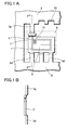
- FIG. 1 depicts collectively a semiconductor device of this invention, with FIG. 1A being a plan view of the semiconductor device and FIG. 1B being a cross-sectional view along line X-X of FIG. 1A.
- FIG. 2 depicts collectively a semiconductor device of this invention, with FIG. 2A being a plan view of the semiconductor device and FIG. 2B being a cross-sectional view along line Y-Y of FIG. 2A.
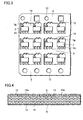
- FIG. 3 is a plan view showing a lower frame of a semiconductor device of this invention.
- FIG. 4 is a plan view showing one whole lower frame of a semiconductor device of this invention.
- FIG. 5 is a plan view showing an upper frame of a semiconductor device of this invention.
- FIG. 6 is a plan view showing one whole upper frame of a semiconductor device of this invention.
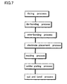
- FIG. 7 shows the process flow of a manufacturing method of this invention.
- FIG. 8 depicts collectively a positioning procedure for a manufacturing method of this invention.
- FIG. 8A is a plan view of an index hole for the positioning formed in the lower frame
- FIG. 8B is a cross-sectional view along line Z-Z in FIG. 8A
- FIG. 8C is a plan view of an index hole for positioning formed in the upper frame.
- FIG. 9 is table of relevant characteristics of the semiconductor devices based on this invention and conventional technology.
- FIG. 10 is a plan view of another embodiment of this invention.
- FIG. 11 depicts an assembling structure of a conventional power switching MOSFET device.
- FIG. 12 depicts an assembling structure of a conventional switching device.
- FIG. 13 depicts another assembling structure of a conventional switching device.
- FIG. 1 and FIG. 2 show an assembling structure of a semiconductor device of this invention.
- the semiconductor device of this invention includes:
- FIG. 1A shows the arrangement of the lower frame 4 and the semiconductor chip 1
- FIG. 1B is a cross-sectional view along line X-X of FIG. 1A of the lower frame 4.
- the lower frame 4 itself is punched out from a copper material.
- the lower frame 4 includes a header 2 located in the center of the lower frame 4, three external leads 3d combined with the header 2 as one unit and extending from the header 2 to the outer frame 9, and an external lead 3g for another electrode 10 with one end being close to the header 2 and another end being connected to the outer frame 9.
- the header 2 and the free end of the external lead 3g for another electrode 10 are lifted a little above the external leads 3d and other portion of the external lead 3g. This is to approximately level all three surfaces of the external leads 3d, 3g, and 3s.
- the small controlling electrode and the current passage electrode 5 occupy most of the surface area of the top face of semiconductor chip 1.
- the bottom face also has a current passage electrode (not shown in the figure) covering the entire surface area.
- the semiconductor chip 1 used can be a power MOSFET as an insulated gate type semiconductor device or an IGBT (Insulated Gate Bipolar Transistor), which is a composite device combining a power MOSFET and transistors.
- a gold electrode is formed as a drain electrode (not shown in the figure) by sputtering on the bottom face of the power MOSFET.
- An aluminum/titanium/nickel/(gold or silver) thin film is evaporated onto the top face of the device to form the gate electrode 10 and source electrode 5.
- the drain electrode and source electrode serve as the current passage electrodes 5, while the gate electrode 10 serves as a controlling electrode for controlling the switching on and off of the channel.
- a bare chip power MOSFET 1 is fixed on a predetermined position within the header 2 of the lower frame 4 using a pre-form material made of solder or silver paste.
- the gate electrode 10 is electrically connected to the external lead 3g, which later becomes a gate terminal, by ball bonding using gold bonding wires 11.
- FIG. 2A shows the arrangement of the upper frame 7 and the semiconductor chip 1
- FIG. 2B is a cross-sectional view along line Y-Y of FIG. 2A of the upper frame 7.
- the upper frame is punched out from a copper material.
- the upper frame 7 includes the connection electrode 6 that is to be fixed on the current passage electrode 5, such as the source electrode, formed on the top face of the semiconductor chip 1 and the external leads 3s combined with the connection electrode 5 as one unit.
- connection electrode 6 It is desirable that the connection electrode 6 have the same shape as the source electrode or the current passage electrode 5 and cover almost all the surface area of the source electrode. However, the surface area covered by the connection electrode 6 may be decided taking positioning accuracy into consideration.
- Two external leads 3s extend from the connection electrode 6 and reach the outer frame 9. The external leads 3s are configured not to contact the four external leads 3d, 3g of the lower frame 4 or the bonding wires 11. At the completion of the manufacturing process, the semiconductor device of this invention will take the form of a SOP6 package.
- the cross-sectional view of the upper frame is shown in FIG. 2B.
- the external leads 3s extending from the connection electrode 6 first bend upwardly, then bend downwardly so that the portion extruding from the resin mold 8 level with the four external leads 3d, 3g of the lower frame 4, and bend upwardly again by the thickness of the lower frame 4 at the portion overlapping with the outer frame 9 of the lower frame 4. Accordingly, cuts 12 are made in the lower frame 4 at the locations where the external leads 3s of the upper frame 7 extend level with other leads.
- connection electrode 6 is then fixed on the source electrode 5 using a pre-form material made of solder or silver paste, with the connection electrode 6 covering the most of the surface area of the source electrode 5.
- the adhesion between the two electrodes improves as the connection electrode 6 is pressed against the source electrode 5 by the spring function of the external leads 3s.
- the resin mold 8 covers the header 2 and a portion of the external leads 3d, 3g of the lower frame 4, and the connection electrode 6 and a portion of the external leads 3s of the upper frame 7.
- the finished semiconductor device of this embodiment has six external leads 3d, 3g, 3c extruding from the resin mold 8 and can be considered as a device composed of one frame.
- FIG. 9 shows the measured on-state resistances of samples C and D of this embodiment.
- the difference of the on-state resistance between the semiconductor device made with solder pre-form fixing the connection electrode 6 of the upper frame 7 and the device made with silver paste pre-form is merely 0.07 m ⁇ , and is not reflected in the difference in material characteristics of the pre-form materials. This is because the pre-form material is extremely thin in comparison to its surface area.
- the method of manufacturing a semiconductor device of this invention includes:
- FIG. 7 shows a process flow of the manufacturing method of this embodiment. It includes from upstream to downstream, a dicing procedure, a die bonding procedure, a wire bonding procedure, an electrode placement procedure, a molding procedure, a solder plating procedure, and a cut and bend procedure.
- a semiconductor wafer (not shown in the figure) having a large number of power MOSFET as the insulating gate type semiconductor component, or IGBTs, as the composite device of a combination of power MOSFETs and transistors, is cut by a dicing saw along the scribing lines into individual semiconductor chips 1.
- the current passage electrode 5 occupying most of the surface area of the semiconductor chip 1 and the small controlling electrode 10 are already formed on the top face of the semiconductor chip 1.
- the whole bottom face of the semiconductor chip 1 is also covered by the current passage electrode.
- a gold electrode is formed by sputtering on the bottom face as a drain electrode (not shown in the figure).
- gate electrode 10 and source electrode 5 An aluminum/titanium/nickel/(gold or silver) thin film is evaporated onto the top face to form the gate electrode 10 and source electrode 5.
- the drain electrode and source electrode 5 serve as the current passage electrodes while the gate electrode 10 serves as a controlling electrode for controlling on and off of the channel.
- the semiconductor chip 1 is fixed on the header 2 of the lower frame 4.
- FIG. 3 and FIG. 4 are the plan views showing the whole lower frame structure 4.
- the lower frame itself is punched out from a copper material.
- the lower frame 4 includes a header 2 located in the center of the lower frame 4, three external leads 3d combined with the header 2 as one unit and extending from the header 2 to the outer frame 9, and an external lead 3g for another electrode 10 with one end being close to the header 2 and another end being connected to the outer frame 9.
- the header 2 and the free end of the external lead 3g for another electrode 10 are lifted a little above the external leads 3d and other portion of the external lead 3g.
- round index holes 12 are formed at both side edges of the outer frame 9 of the lower frame 4 with a constant interval for each side. These index holes are used for the positioning and the pitch-by-pitch transportation in the procedures of the manufacturing method.
- a square position-determining index hole 13m (shown in FIG. 4) for positioning the upper and lower frames 4, 7 is formed next to each round index hole 12 along the top side edge of the outer frame 9 of the lower frame.
- the round index holes 12 are formed at the locations corresponding to the lines connecting the centers of the headers 2 with a constant interval along the bottom side edge of the outer frame 9 of the lower frame 4.
- Two headers 2 and the corresponding external leads 3d are formed in one cell area 14 surrounded by the outer frame 9.
- the lower frame 4 has a 3 x 20 matrix of cell areas 14 between the top and bottom rows of index holes 12.
- one lower frame 4 has 60 cell areas and 120 headers 2 for fixing the semiconductor chips 1.
- the headers 2 and the external leads 3d are omitted from the cell areas 14.
- the semiconductor chips 1 are then fixed on each of the headers 2 in the cell areas 14 of the lower frame 4 by die bonding. That is, the semiconductor chips 1, such as power MOSFET bare chips, are fixed on the headers 2 of the lower frame 4 through the pre-form made of solder or silver paste using a die bonding instrument. During this procedure, the index holes 12 in the top and bottom side edges are used for the positioning of the headers 2 and for transporting the lower frame 4 by one pitch at a time. At the end, all the headers 2 of the lower frame 4 have a semiconductor chip fixed on themselves.
- molten solder is applied on the header 2 by melting a solder wire, then, the semiconductor chip 1 is placed on the header 2 and cooled down for completing the fixing.
- a viscous silver paste is applied on the header 2, then, the semiconductor chip 1 is temporarily fixed on the header 2 and later heated in a non-oxidation atmosphere for curing of the paste and completing the fixing.
- another electrode 10, such as the gate electrode, of the semiconductor chip 1 is bonded to the corresponding external lead 3g with a metal wire 11.
- Another electrodes 10 including the gate electrodes are electrically connected by ball bonding with gold bonding wires using a bonding instrument with automatic recognition.
- the index holes 12 in the top and bottom side edges are also used for the positioning of the headers 2 and for transporting the lower frame 4 by one pitch at a time.
- all of another electrodes 10 including the gate electrodes of the semiconductor chip 1 of the lower frame 4 are automatically bonded to the corresponding external leads 3g.
- the electrode placement procedure includes preparing an upper frame 7 having a connection electrode 6 to be fixed on a current passage electrode 5 formed on the top face of the semiconductor chip 1 and having external leads 3s combined with the connection electrode 6 as one unit, and positioning the lower frame 4 and the upper frame 7 and for fixing the connection electrode 6 of the upper frame 7 on the current passage electrode 5 of the semiconductor chip 1.
- FIG. 5 and FIG. 6 are plan views showing the whole upper frame structure 7.
- the upper frame 7 itself is punched out from a copper material.
- the upper frame 7 includes the connection electrode 6 to be fixed on the current passage electrode 5, such as the source electrode, formed on the top face of the semiconductor chip 1 and the external leads 3s combined with the connection electrode 5 as one unit.
- connection electrode 6 It is desirable that the connection electrode 6 have the same shape as the source electrode, or the current passage electrode 5, and cover almost all the surface area of the source electrode. However, the surface area covered by the connection electrode 6 may be decided taking positioning accuracy into consideration.
- Two external leads 3s extend from the connection electrode 6 and reach the outer frame 9. The external leads 3s are configured not to contact the four external leads 3d, 3g of the lower frame 4 or the bonding wires 11.
- the semiconductor device of the present invention will take the form of a SOP6 configuration.
- the cross-sectional view of the upper frame is shown in FIG. 2B.
- the external leads 3s extending from the connection electrode 6, first bend upwardly, then bend downwardly so that the portion protruding from the resin mold 8 level with the four external leads 3d, 3g of the lower frame 4, and bend upwardly again by the thickness of the lower frame 4 at the portion overlapping with the outer frame 9 of the lower frame 4. Accordingly, cuts 12 are made in the lower frame 4 at the locations where the external leads 3s of the upper frame 7 extend leveling with other leads.
- round index holes 12 are also formed at both side edges of the outer frame 9 of the upper frame 7 with a constant interval for each side, as in the case with the lower frame 4. These index holes are used for the positioning and the pitch-by-pitch transportation in the manufacturing method.
- a square position-determining index hole 13u for positioning the upper and lower frames 4, 7 is formed next to each round index hole 12 along the top side edge of the outer frame 9 of the upper frame 7.
- the two position-determining index holes 13m, 13u have an identical size and shape. The role of the two position-determining index holes in the positioning procedure will be described in detail later in this description of the manufacturing method.
- Two connection electrodes 6 and the corresponding external leads 3s are formed in one cell area 14 surrounded by the outer frame 9.
- the upper frame 7 also has a 3 x 20 matrix of cell areas 14 between the top and bottom rows of index holes 12 in accordance with the alignment in the lower frame 4.
- one upper frame 7 has 60 cell areas and 120 connection electrodes 6.
- the connection electrodes 6 and the external leads 3s are omitted from the cell areas 14.
- the lower frame 4 and the upper frame 7 are brought to a proper position for the assembling. That is, the upper frame 4 is put over the lower frame 7 so that the two position-determining index holes 13m, 13u coincide.
- FIG. 8A and 8B are plan and side views, respectively, of the position-determining index hole 13m formed in the lower frame 4.
- the position-determining index hole 13m in the lower frame 4 has four guiding portions 13G bent upward at the four edges of the square hole.
- the guiding portions 13G are inserted into the position-determining index holes 13u of the upper frame 7, which is shown in FIG. 8C and has the same size and shape as the position-determining index holes 13m of the lower frame 4.
- the height of the guiding portion 13G is designed to be small enough to prevent malfunctions during the pitch-by-pitch transportation of the lower frame 4 in the manufacturing procedures such as die bonding and wire bonding.
- guiding pins (not shown in the figure) as separate parts from the frames can be used for positioning the upper and lower frames 4, 7, replacing the guiding portions 13G. That is, the guiding pins are inserted into the round index hole 12 of the two frames or the square position-determining index holes 13m, 13u which have, in this case, exactly same shape and size, for positioning the upper and lower frames 4, 7. Since this configuration is free from the guiding portion 13G, there will not be any malfunctions due to the guiding portion 13G during the pitch-by-pitch transportation of the lower frame 4 in the manufacturing procedures such as die bonding and wire bonding.
- connection electrodes 6 of the upper frame 7 are located right above the current passage electrodes 5 including the source electrode, and are fixed on the current passage electrodes 5 through the pre-form made of solder or silver paste.
- the adhesion between the two electrodes improves as the connection electrode 6 is pressed against the current passage electrode 5 by the spring function of the external leads 3s.
- Other processing conditions are similar to those of the die bonding procedure.
- the insulating resin 8 such as epoxy resin, covers the header 2 and a portion of the external leads 3d, 3g of the lower frame 4, the connection electrode 6 and a portion of the external leads 3s of the upper frame 7, and the semiconductor chip 1, using the transfer molding technique.
- the finished semiconductor device of this embodiment has six external leads 3d, 3g, 3c extruding from the resin mold 8 and can be considered as a device composed of one frame, taking the form of a SOP6 package.
- the external leads 3d, 3g, 3s extruding from the resin mold 8 are coated with solder metals such as tin using the solder plating, in preparation for mounting on a circuit board.
- the individual semiconductor devices are separated by cutting the external leads 3d, 3g, 3s of the two frames 4, 7 from the outer frames 9 of the two frames 4, 7, by using cutting metal dies. Later, if needed, the external leads 3d, 3g, 3s extruding from the resin mold 8 are pressed into predetermined shapes.
- FIG. 10 Another embodiment of the method of manufacturing a semiconductor device of this invention is shown in FIG. 10.
- the wire bonding is completely eliminated from the manufacturing process.
- the upper frame 7 has another connection electrode 15 that is to be fixed on another electrode 10, such as a gate electrode, of the semiconductor chips 1, and has another external lead 3g extending to the frame which is combined with the connection electrode as one unit.
- the gate connection electrode 15 is fixed, together with the fixing of the connection electrode, on the gate electrode 10 using the pre-form during the electrode placement procedure. Because of the need for a larger gate electrode 10 than the gate electrode 10 used with the wire bonding technique due to the accuracy of the positioning, in this embodiment the surface area of the current passage electrode 5 becomes smaller, resulting in an on-state resistance that is higher by a small amount.
- this manufacturing method of a semiconductor device has a significant advantage in that the total manufacturing process is shortened by eliminating all the wire bonding processes.
- this invention is not confined to the SOP6 type package, and can also be applied to a SOP8 package and the configuration where two semiconductor chips are housed inside one package.
Landscapes
- Wire Bonding (AREA)
- Lead Frames For Integrated Circuits (AREA)
- Connection Of Batteries Or Terminals (AREA)
Abstract
Description
Claims (17)
- A semiconductor device comprising:characterized in that it further comprises:a lower frame (4) having a header (2) for fixing a semiconductor chip (1) thereon and having external leads (3d) combined with said header (2) as one unit; anda semiconductor chip (1) fixed on said header (2);an upper frame (7) having a connection electrode (6) fixed on a current passage electrode (5) formed on the top face of said semiconductor chip (1) and having external leads (3s) combined with said connection electrode (6) as one unit; anda resin mold (8) covering said header (2) and a portion of said external leads (3d) of said lower frame (4) , and covering said connection electrode (6) and a portion of said external leads (3s) of said upper frame (7).
- A semiconductor device according to claim 1, characterized in that said semiconductor chip (1) is composed of insulated gate type semiconductor components.
- A semiconductor device according to claim 1, characterized in that said semiconductor chip (1) is composed of MOSFET or IGBT.
- A semiconductor device according to anyone of claims 1-3, characterized in that said header (2) and said external leads (3d) of said lower frame (4) are formed from a single frame material.
- A semiconductor device according to anyone of claims 1-4, characterized in that said connection electrode (6) and said external leads (3s) of said upper frame (7) are formed from a single frame material.
- A semiconductor device according to anyone of claims 1-5, characterized in that said lower frame (4) has an external lead (3g) for the electric connection to a gate electrode (10).
- A semiconductor device according to anyone of claims 1-6, characterized in that said upper frame (7) has a gate connection electrode (15) fixed on a gate electrode (10) and an external lead (3g) combined with said gate connection electrode (15) as one unit.
- A manufacturing method of semiconductor device comprising:preparing a lower frame having a header for fixing a semiconductor chip thereon and having external leads combined with said header as one unit; andfixing a semiconductor chip on said header; characterized in that the manufacturing method further comprises:preparing an upper frame having a connection electrode fixed on a current passage electrode formed on the top face of said semiconductor chip and having external leads combined with said connection electrode as one unit;positioning said lower frame and said upper frame and for fixing said connection electrode of said upper frame on said current passage electrode of said semiconductor chip;creating a mold with an insulating resin covering said header and a portion of said external leads of said lower frame, covering said connection electrode and a portion of said external leads of said upper frame, and covering said semiconductor chip.
- A manufacturing method of semiconductor device according to claim 8, characterized in that said positioning of said lower frame and said upper frame is performed by inserting protruding portions made from surrounding portion of holes formed as indices in said lower frame into index holes in said upper frame
- A manufacturing method of semiconductor device according to claim 8 or 9, wherein an external lead for another electrode of said semiconductor chip is formed close to said header in said lower frame.
- A manufacturing method of semiconductor device according to claim 10, wherein said another electrode of said semiconductor chip and said external lead are wire-bonded with metal wires after fixing said semiconductor chip on said header.
- A manufacturing method of semiconductor device according to anyone of claims 8-11, characterized in that in parallel with said connection electrode and said external leads combined with said connection electrode as one unit are formed in said upper frame another connection electrode for another electrode of said semiconductor chip and another external lead combined with said another connection electrode as one unit.
- A manufacturing method of semiconductor device according to claim 12, characterized in that said another connection electrode of said upper frame is fixed on said another electrode of said semiconductor device at the same time as said connection electrode is fixed on said current passage electrode of said semiconductor chip.
- A manufacturing method of semiconductor device according to claim 8, 9, 10, 11, 12, or 13, characterized in that said semiconductor chip is composed of insulated gate type semiconductor components.
- A manufacturing method of semiconductor device according to claim 8, 9, 10, 11, 12, or 13, characterized in that said semiconductor chip is composed of MOSFET or IGBT.
- A manufacturing method of semiconductor device according to anyone of claims 8-15, characterized in that said header and said external leads of said lower frame are formed from a single frame material.
- A manufacturing method of semiconductor device according to anyone of claims 8-16, characterized in that said connection electrode and said external leads of said upper frame are formed from a single frame material.
Applications Claiming Priority (2)
| Application Number | Priority Date | Filing Date | Title |
|---|---|---|---|
| JP2000083879 | 2000-03-24 | ||
| JP2000083879A JP3510838B2 (en) | 2000-03-24 | 2000-03-24 | Semiconductor device and manufacturing method thereof |
Publications (2)
| Publication Number | Publication Date |
|---|---|
| EP1137065A2 true EP1137065A2 (en) | 2001-09-26 |
| EP1137065A3 EP1137065A3 (en) | 2003-10-01 |
Family
ID=18600439
Family Applications (1)
| Application Number | Title | Priority Date | Filing Date |
|---|---|---|---|
| EP01107266A Withdrawn EP1137065A3 (en) | 2000-03-24 | 2001-03-23 | Semiconductor device and manufacturing method thereof |
Country Status (5)
| Country | Link |
|---|---|
| US (1) | US6689642B2 (en) |
| EP (1) | EP1137065A3 (en) |
| JP (1) | JP3510838B2 (en) |
| KR (1) | KR100381683B1 (en) |
| TW (1) | TWI239089B (en) |
Families Citing this family (14)
| Publication number | Priority date | Publication date | Assignee | Title |
|---|---|---|---|---|
| US6617655B1 (en) * | 2002-04-05 | 2003-09-09 | Fairchild Semiconductor Corporation | MOSFET device with multiple gate contacts offset from gate contact area and over source area |
| JP2004079760A (en) | 2002-08-19 | 2004-03-11 | Nec Electronics Corp | Semiconductor device and assembling method thereof |
| JP4728327B2 (en) * | 2004-05-18 | 2011-07-20 | シルバーブルック リサーチ ピーティワイ リミテッド | Trading terminal |
| US7678680B2 (en) * | 2004-06-03 | 2010-03-16 | International Rectifier Corporation | Semiconductor device with reduced contact resistance |
| JP2006100481A (en) * | 2004-09-29 | 2006-04-13 | Nec Electronics Corp | Semiconductor device |
| US7602054B2 (en) * | 2005-10-05 | 2009-10-13 | Semiconductor Components Industries, L.L.C. | Method of forming a molded array package device having an exposed tab and structure |
| US7447041B2 (en) * | 2007-03-01 | 2008-11-04 | Delphi Technologies, Inc. | Compression connection for vertical IC packages |
| CN101446620B (en) * | 2007-11-28 | 2011-04-06 | 中国科学院半导体研究所 | Battery-based semiconductor AC differential conductive scanning measurement system |
| US8076183B2 (en) * | 2009-10-27 | 2011-12-13 | Alpha And Omega Semiconductor, Inc. | Method of attaching an interconnection plate to a semiconductor die within a leadframe package |
| TWI381921B (en) * | 2009-12-08 | 2013-01-11 | Zhen Ding Technology Co Ltd | Punching method |
| US8513784B2 (en) * | 2010-03-18 | 2013-08-20 | Alpha & Omega Semiconductor Incorporated | Multi-layer lead frame package and method of fabrication |
| US8581376B2 (en) * | 2010-03-18 | 2013-11-12 | Alpha & Omega Semiconductor Incorporated | Stacked dual chip package and method of fabrication |
| US8436429B2 (en) | 2011-05-29 | 2013-05-07 | Alpha & Omega Semiconductor, Inc. | Stacked power semiconductor device using dual lead frame and manufacturing method |
| JP7763964B2 (en) * | 2022-09-14 | 2025-11-04 | 三菱電機株式会社 | Semiconductor device and method for manufacturing the same |
Family Cites Families (9)
| Publication number | Priority date | Publication date | Assignee | Title |
|---|---|---|---|---|
| US4496965A (en) * | 1981-05-18 | 1985-01-29 | Texas Instruments Incorporated | Stacked interdigitated lead frame assembly |
| US4801765A (en) * | 1986-01-06 | 1989-01-31 | American Telephone And Telegraph Company, At&T Bell Laboratories | Electronic component package using multi-level lead frames |
| JP3088193B2 (en) * | 1992-06-05 | 2000-09-18 | 三菱電機株式会社 | Method for manufacturing semiconductor device having LOC structure and lead frame used therein |
| US5521427A (en) * | 1992-12-18 | 1996-05-28 | Lsi Logic Corporation | Printed wiring board mounted semiconductor device having leadframe with alignment feature |
| US5506174A (en) * | 1994-07-12 | 1996-04-09 | General Instrument Corp. | Automated assembly of semiconductor devices using a pair of lead frames |
| US5920113A (en) * | 1996-08-13 | 1999-07-06 | Motorola, Inc. | Leadframe structure having moveable sub-frame |
| US6040626A (en) * | 1998-09-25 | 2000-03-21 | International Rectifier Corp. | Semiconductor package |
| US6256200B1 (en) * | 1999-05-27 | 2001-07-03 | Allen K. Lam | Symmetrical package for semiconductor die |
| US6307755B1 (en) * | 1999-05-27 | 2001-10-23 | Richard K. Williams | Surface mount semiconductor package, die-leadframe combination and leadframe therefor and method of mounting leadframes to surfaces of semiconductor die |
-
2000
- 2000-03-24 JP JP2000083879A patent/JP3510838B2/en not_active Expired - Lifetime
-
2001
- 2001-03-15 TW TW090106044A patent/TWI239089B/en not_active IP Right Cessation
- 2001-03-23 EP EP01107266A patent/EP1137065A3/en not_active Withdrawn
- 2001-03-23 KR KR10-2001-0015111A patent/KR100381683B1/en not_active Expired - Fee Related
- 2001-03-23 US US09/814,942 patent/US6689642B2/en not_active Expired - Lifetime
Also Published As
| Publication number | Publication date |
|---|---|
| KR20010090520A (en) | 2001-10-18 |
| KR100381683B1 (en) | 2003-04-26 |
| EP1137065A3 (en) | 2003-10-01 |
| JP3510838B2 (en) | 2004-03-29 |
| US6689642B2 (en) | 2004-02-10 |
| US20010029063A1 (en) | 2001-10-11 |
| TWI239089B (en) | 2005-09-01 |
| JP2001274309A (en) | 2001-10-05 |
Similar Documents
| Publication | Publication Date | Title |
|---|---|---|
| US6777786B2 (en) | Semiconductor device including stacked dies mounted on a leadframe | |
| US9218987B2 (en) | Method for top-side cooled semiconductor package with stacked interconnection plates | |
| US6476481B2 (en) | High current capacity semiconductor device package and lead frame with large area connection posts and modified outline | |
| US6756658B1 (en) | Making two lead surface mounting high power microleadframe semiconductor packages | |
| US8076183B2 (en) | Method of attaching an interconnection plate to a semiconductor die within a leadframe package | |
| US7868432B2 (en) | Multi-chip module for battery power control | |
| US6689642B2 (en) | Semiconductor device and manufacturing method thereof | |
| US8343811B2 (en) | Semiconductor device | |
| EP2058857A2 (en) | IC chip package with directly connected leads | |
| US20050121799A1 (en) | Semiconductor device manufacturing method and semiconductor device manufactured thereby | |
| US7663212B2 (en) | Electronic component having exposed surfaces | |
| US20120181676A1 (en) | Power semiconductor device packaging | |
| US20250316633A1 (en) | High thermal dissipation, packaged electronic device and manufacturing process thereof | |
| US20130017652A1 (en) | Method of manufacturing a semiconductor device package with a heatsink | |
| JP3650008B2 (en) | Protection circuit device using MOSFET and manufacturing method thereof | |
| US20040099940A1 (en) | Semiconductor device having clips for connecting to external elements | |
| US12519042B2 (en) | Methods for manufacturing a semiconductor package and a semiconductor module | |
| US7274092B2 (en) | Semiconductor component and method of assembling the same | |
| EP4227995B1 (en) | Power electronics module and method for its manufacturing | |
| JP2002368219A (en) | One-chip dual type insulated gate type semiconductor device | |
| US20120181677A1 (en) | Semiconductor device package with two component lead frame | |
| US20240030200A1 (en) | Semiconductor package and method | |
| US20260082944A1 (en) | Semiconductor device and method for manufacturing the same | |
| EP3955289A1 (en) | Four terminal transistor package | |
| JP2003124260A (en) | Semiconductor device |
Legal Events
| Date | Code | Title | Description |
|---|---|---|---|
| PUAI | Public reference made under article 153(3) epc to a published international application that has entered the european phase |
Free format text: ORIGINAL CODE: 0009012 |
|
| AK | Designated contracting states |
Kind code of ref document: A2 Designated state(s): AT BE CH CY DE DK ES FI FR GB GR IE IT LI LU MC NL PT SE TR |
|
| AX | Request for extension of the european patent |
Free format text: AL;LT;LV;MK;RO;SI |
|
| RIN1 | Information on inventor provided before grant (corrected) |
Inventor name: FUKUDA, HIROKAZU |
|
| PUAL | Search report despatched |
Free format text: ORIGINAL CODE: 0009013 |
|
| AK | Designated contracting states |
Kind code of ref document: A3 Designated state(s): AT BE CH CY DE DK ES FI FR GB GR IE IT LI LU MC NL PT SE TR |
|
| AX | Request for extension of the european patent |
Extension state: AL LT LV MK RO SI |
|
| 17P | Request for examination filed |
Effective date: 20040331 |
|
| 17Q | First examination report despatched |
Effective date: 20040506 |
|
| AKX | Designation fees paid |
Designated state(s): DE FR GB |
|
| 17Q | First examination report despatched |
Effective date: 20040506 |
|
| STAA | Information on the status of an ep patent application or granted ep patent |
Free format text: STATUS: THE APPLICATION IS DEEMED TO BE WITHDRAWN |
|
| 18D | Application deemed to be withdrawn |
Effective date: 20141001 |