EP1136941A1 - Tragbare Datenträgeranordnung - Google Patents
Tragbare Datenträgeranordnung Download PDFInfo
- Publication number
- EP1136941A1 EP1136941A1 EP00106472A EP00106472A EP1136941A1 EP 1136941 A1 EP1136941 A1 EP 1136941A1 EP 00106472 A EP00106472 A EP 00106472A EP 00106472 A EP00106472 A EP 00106472A EP 1136941 A1 EP1136941 A1 EP 1136941A1
- Authority
- EP
- European Patent Office
- Prior art keywords
- module
- data
- data carrier
- carrier arrangement
- control unit
- Prior art date
- Legal status (The legal status is an assumption and is not a legal conclusion. Google has not performed a legal analysis and makes no representation as to the accuracy of the status listed.)
- Withdrawn
Links
Images

Classifications
-
- G—PHYSICS
- G06—COMPUTING OR CALCULATING; COUNTING
- G06K—GRAPHICAL DATA READING; PRESENTATION OF DATA; RECORD CARRIERS; HANDLING RECORD CARRIERS
- G06K19/00—Record carriers for use with machines and with at least a part designed to carry digital markings
- G06K19/06—Record carriers for use with machines and with at least a part designed to carry digital markings characterised by the kind of the digital marking, e.g. shape, nature, code
- G06K19/067—Record carriers with conductive marks, printed circuits or semiconductor circuit elements, e.g. credit or identity cards also with resonating or responding marks without active components
- G06K19/07—Record carriers with conductive marks, printed circuits or semiconductor circuit elements, e.g. credit or identity cards also with resonating or responding marks without active components with integrated circuit chips
-
- G—PHYSICS
- G06—COMPUTING OR CALCULATING; COUNTING
- G06K—GRAPHICAL DATA READING; PRESENTATION OF DATA; RECORD CARRIERS; HANDLING RECORD CARRIERS
- G06K19/00—Record carriers for use with machines and with at least a part designed to carry digital markings
- G06K19/06—Record carriers for use with machines and with at least a part designed to carry digital markings characterised by the kind of the digital marking, e.g. shape, nature, code
- G06K19/067—Record carriers with conductive marks, printed circuits or semiconductor circuit elements, e.g. credit or identity cards also with resonating or responding marks without active components
- G06K19/07—Record carriers with conductive marks, printed circuits or semiconductor circuit elements, e.g. credit or identity cards also with resonating or responding marks without active components with integrated circuit chips
- G06K19/073—Special arrangements for circuits, e.g. for protecting identification code in memory
Definitions
- the invention relates to a portable data carrier arrangement a data memory and a control unit, each as Integrated circuit are executed, the control unit with means of connecting to an external one Read and write unit is provided.
- Disk arrangements are data exchange and data processing systems with one Numerous such portable data carrier arrangements are known, which as needed with a read and write unit in Can be connected to exchange data can.
- Disk arrangements of the type mentioned, in addition to sufficient storage capacity even with a control unit are not only interactive Data and signal exchange with the external read and write unit, but also decentralized data processing and storage in the individual, intelligent data carrier arrangements, which is extremely diverse and result in highly developed applications.
- Such disk arrangements are typically in card form (for Example in credit card format) with embedded integrated Circuit modules executed (so-called chip cards).
- EP 0 337 185 B1 is a portable one Disk arrangement known that a control unit and has a data memory, the control unit and the Data carriers each run as an integrated circuit are.
- the control unit has means for establishing a connection to an external read and write unit. It is still an additional data storage on the portable Provided data carrier, its control by the control unit self-sufficient is protected by coding.
- the integrated circuits can be in two or more, by Lines connected blocks divided or on a single Substrate. There are both so-called “Multi-chip” or “single-chip versions” conceivable.
- the problem described at the beginning also lies in EP 0 337 185 B1 before.
- the object of the present invention is therefore to the digitized stored on a portable data carrier Data against copying without loss of quality protect.
- the invention is based on the finding that copying of analog data in contrast to digital data is not critical.
- control unit generates at least one analog signal. At least an analog signal to the external read and write unit can then be transmitted by the users at will be tapped. Copies made by the digitized Data that are present in the data memory are produced, are, however, of significantly lower quality than the original.
- the control unit In order to enable tapping of the at least one analog signal, has the means to connect a plurality of contacts, at least one of the for Data transfer contacts provided with a digital-to-analog converter the control unit is connected. So it is conceivable, provided that the data is connected to one of the Contacts are made available to this data signal to fully analogize. However, it could also be just a few Bits (for example the "most significant bit” MSB) are analogized become. With parallel data transmission via in the simplest case, a plurality of contacts is sufficient, to analogize a data signal. But then it would be also conceivable, each of the data signals transmitted in parallel to be made available as an analog signal at the contacts. In this case, the best possible protection against a quality-free copy the digitized data in the data storage ensured.
- the control unit decodes those received from the data memory Data. It is advantageous in the data memory and Control unit one processor each for the backed up means coded or encrypted, data exchange assigned. This is intended to prevent unauthorized access to the digitized Data in the data storage or on one of the connecting lines to the control unit can be prevented.
- the first and the second module are advantageously for Intended function of the portable data carrier arrangement one above the other firmly connected so that contact points of the integrated circuits in the first and in the second module are electrically connected.
- one optionally encrypted data transmission between the first and the second module finds mutual authentication of the two modules instead.
- a review can be based on physical effects, for example a capacity, optical properties of the first and second Module, an inductance, a current consumption or a Time behavior.
- security can be increased if the spatial proximity of the first and the second Module is checked before data exchange between the first and the second module is enabled. The verification The spatial proximity of the two modules takes place advantageously takes place before the authentication.
- Verification of authenticity and proximity ensured is, for example, according to the so-called Diffie-Hillman method a common key can be agreed. There are unwanted attacks on the digitized data in the arrangement according to the invention against the Diffie-Hillman method not possible.
- the first module means to connect to a external read and write unit. In this case it is possible to write data directly into the data storage without to have to do an analog-to-digital conversion.
- FIG. 1 shows the top view of a first main page 12 a first module 2 of the portable data carrier arrangement according to the invention.
- first module 2 From the first main page 12 is in first module 2 introduced a recess 16.
- the in the area of the first module 2 running side edges of the recess 16 are angled such that the side edge in the plane of the first main surface 12 further from the outer edge of the first module 2 is removed than that inside the first Module 2 lying side edge. This is particularly evident from the Cross section of Figure 3 well.
- the first module 2 points furthermore a semiconductor chip 6, which has a data memory contains.
- the semiconductor chip 6 faces the first Main page of module 2 facing side contact points 10 on.
- the semiconductor chip 6 can be connected via these contact points 10 be contacted.
- the contact points 10 can for example also via conductor tracks with appropriate contact pads of the Semiconductor chips 6 are connected. Furthermore, on the first module 2 provided a plurality of contacts 9, the (within the housing) connected to the semiconductor chip 6 are. Only digitized data can be obtained via the contacts 9 are written in the semiconductor chip 6. A reading of Data from the data memory in the semiconductor chip 6 via the However, contacts 9 is not possible.
- FIG 2 shows the top view of a second module 3 of FIG Portable data carrier arrangement according to the invention shown.
- the side edges of the second module 3 are on the course of the Adjusted side edges of the recess 16.
- the second module 3 can thus in the recess 16 from the side edge 25 in the first module 2 are inserted.
- There is an embodiment of the first and the second module possible that the second module 3 snaps into the first module 2.
- Via a recess 17, which is shown in Figure 1, can the second module 3, for example, again in the direction of the side edge 25 moved and removed from module 2.
- the second module 3 has a semiconductor chip 7 with a Control unit on, via contact points 11 from the outside is electrically contactable.
- the second module is located 3 in the first module 2 there are the contact points 10 and 11 the semiconductor chips 6 and 7 lie exactly one above the other.
- the semiconductor chips 6 and 7 thus face each other to lie in the data carrier arrangement.
- Figure 5 in which a cross section through the invention Disk arrangement is shown.
- the semiconductor chip 7 decodes and decompresses the received from the data memory (in the semiconductor chip 6) Data and carries at least one data signal via a digital-to-analog converter a contact 8, which can be contacted from the outside is. Be through a single or some of the contacts 8 Transfer data to an external writing and reading device. The remaining contacts 8 are used for the semiconductor chip 7 to be provided with a supply potential and Exchange tax data.
- a data exchange between the semiconductor chip 6 and the Semiconductor chip 7 only takes place if, on the one hand, the spatial proximity of the first and second modules 2, 3 checked and then mutual authentication by one arranged in each case in the semiconductor chips 6, 7 Processor has taken place.
- An authenticity check that is, the actual togetherness of the first and the second module 2, 3 can for example be based on physical properties. To do this the checking of capacities, inductors, Time behavior when signals occur, optical Properties or a specified current consumption.
- the first and second modules 2, 3 could be attached basically done in any way.
- An attachment could for example via magnetism or via adhesion.
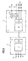
- FIG. 6 shows schematically the operation of the invention portable disk assembly.
- the first module 2 has a semiconductor chip that has a data memory and includes a processor for authentication. It is also conceivable, the data storage and the processor for authentication in separate semiconductor chips on the first module accommodate. Via contacts 9, data can be stored in the data memory be written via an external read / write device. Reading the data from the data memory 5 via the However, contacts 9 is not possible.
- the second module 3 also has a semiconductor chip 7 on which is a processor for authentication, a decoding or decompression and one accordingly desired number of digital-to-analog converters 22 having.
- the components listed could each be based on the second module 3 housed in a plurality of semiconductor chips and be connected to each other via conductor tracks.
- Each of the digital-to-analog converters has one on the output side Contact 8 connected to which then an analog output signal can be tapped. A reliable copy protection is already achieved when only one data signal on the Contact 8 is in analog form. Will the data be parallel made available via a plurality of contacts 8, each of these contacts could be with a digital to analog converter be connected and thus make an analog signal available.
- the analog signals include for example one or more of the most significant Bits of the digital signal in the data memory. The corresponding Bits of the digital signal are then transmitted omitted.
Landscapes
- Engineering & Computer Science (AREA)
- Computer Hardware Design (AREA)
- Microelectronics & Electronic Packaging (AREA)
- Physics & Mathematics (AREA)
- General Physics & Mathematics (AREA)
- Theoretical Computer Science (AREA)
- Computer Security & Cryptography (AREA)
- General Engineering & Computer Science (AREA)
- Storage Device Security (AREA)
Abstract
Description
- Figur 1
- eine Draufsicht auf das erste Modul der erfindungsgemäßen tragbaren Datenträgeranordnung,
- Figur 2
- eine Draufsicht auf das zweite Modul der erfindungsgemäßen Datenträgeranordnung,
- Figur 3
- einen Querschnitt durch das erste Modul aus Figur 1,
- Figur 4
- einen Querschnitt durch das zweite Modul aus Figur 2,
- Figur 5
- einen Querschnitt durch die zusammengesetzten ersten und zweiten Module der Datenträgeranordnung und
- Figur 6
- eine schematische Darstellung der erfindungsgemäßen Datenträgeranordnung.
- 1
- Tragbare Datenträgeranordnung
- 2
- Erstes Modul
- 3
- Zweites Modul
- 4
- Datenspeicher
- 5
- Steuereinheit
- 6
- Halbleiterchip
- 7
- Halbleiterchip
- 8
- Kontakte
- 9
- Kontakte
- 10
- Kontaktstelle
- 11
- Kontaktstelle
- 12
- Erste Hauptseite
- 13
- Zweite Hauptseite
- 14
- Erste Hauptseite
- 15
- Zweite Hauptseite
- 16
- Ausnehmung
- 17
- Vertiefung
- 18
- Digitales Eingangssignal
- 19
- Authentifikation
- 20
- Authentifikation
- 21
- Dekodierung/Dekomprimierung
- 22
- Digital-Analogwandler
- 23
- Analoges Ausgangssignal
- 24
- Signal (analog oder digital)
- 25
- Seitenkante
Claims (9)
- Tragbare Datenträgeranordnung mit einem Datenspeicher (4) und einer Steuereinheit (5), die jeweils als integrierte Schaltung ausgeführt sind, wobei die Steuereinheit (5) mit Mitteln zur Verbindungsherstellung (8) zu einer externen Schreib- und Leseeinheit versehen ist,
dadurch gekennzeichnet, daß die Steuereinheit (5) zumindest ein analoges Signal (23) erzeugt. - Tragbare Datenträgeranordnung nach Anspruch 1,
dadurch gekennzeichnet, daß das zumindest eine analoge Signal (23) an die externe Schreib- und Leseeinheit übertragen wird. - Tragbare Datenträgeranordnung nach Anspruch 1 oder 2,
dadurch gekennzeichnet, daß die Mittel zur Verbindungsherstellung eine Mehrzahl an Kontakten (8) aufweisen, wobei zumindest einer der zur Übertragung von Daten vorgesehenen Kontakte (8) mit einem Digital-Analogwandler in der Steuereinheit verbunden ist. - Tragbare Datenträgeranordnung nach einem der Ansprüche 1 bis 3,
dadurch gekennzeichnet, daß die Steuereinheit (5) die von dem Datenspeicher (4) empfangenen Daten dekomprimiert und/oder dekodiert. - Tragbare Datenträgeranordnung nach einem der Ansprüche 1 bis 4,
dadurch gekennzeichnet, daß im Datenspeicher (4) und der Steuereinheit (5) jeweils ein Prozessor (19, 20) zum gesicherten (kodierten oder verschlüsselten) Datenaustausch zugeordnet ist. - Tragbare Datenträgeranordnung nach einem der Ansprüche 1 bis 5,
dadurch gekennzeichnet, daß die tragbare Datenträgeranordnung aus einem ersten und einem zweiten Modul (2, 3) besteht, die miteinander lösbar verbindbar sind, wobei in dem ersten Modul der Datenspeicher und in dem zweiten Modul die Steuereinheit mit den Mitteln zur Verbindungsherstellung untergebracht ist. - Tragbare Datenträgeranordnung nach Anspruch 6,
dadurch gekennzeichnet, daß das erste und das zweite Modul (2, 3) zur bestimmungsgemäßen Funktion der Datenträgeranordnung übereinanderliegend fest verbunden sind, so daß Kontaktstellen (8, 9) der integrierten Schaltungen in dem ersten und in dem zweiten Modul (2, 3) elektrisch leitend verbunden sind. - Tragbare Datenträgeranordnung nach Anspruch 6 oder 7,
dadurch gekennzeichnet, daß die räumliche Nähe des ersten und des zweiten Moduls (2, 3) überprüft wird, bevor ein Datenaustausch zwischen dem ersten und dem zweiten Modul möglich ist. - Tragbare Datenträgeranordnung nach einem der Ansprüche 1 bis 8,
dadurch gekennzeichnet, daß das erste Modul (2) Mittel zur Verbindungsherstellung (9) zu einer externen Schreib- und Leseeinheit aufweist.
Priority Applications (2)
| Application Number | Priority Date | Filing Date | Title |
|---|---|---|---|
| EP00106472A EP1136941A1 (de) | 2000-03-24 | 2000-03-24 | Tragbare Datenträgeranordnung |
| PCT/DE2001/000693 WO2001073683A1 (de) | 2000-03-24 | 2001-02-22 | Tragbare datenträgeranordnung |
Applications Claiming Priority (1)
| Application Number | Priority Date | Filing Date | Title |
|---|---|---|---|
| EP00106472A EP1136941A1 (de) | 2000-03-24 | 2000-03-24 | Tragbare Datenträgeranordnung |
Publications (1)
| Publication Number | Publication Date |
|---|---|
| EP1136941A1 true EP1136941A1 (de) | 2001-09-26 |
Family
ID=8168235
Family Applications (1)
| Application Number | Title | Priority Date | Filing Date |
|---|---|---|---|
| EP00106472A Withdrawn EP1136941A1 (de) | 2000-03-24 | 2000-03-24 | Tragbare Datenträgeranordnung |
Country Status (2)
| Country | Link |
|---|---|
| EP (1) | EP1136941A1 (de) |
| WO (1) | WO2001073683A1 (de) |
Citations (6)
| Publication number | Priority date | Publication date | Assignee | Title |
|---|---|---|---|---|
| US4677657A (en) * | 1984-07-31 | 1987-06-30 | Omron Tateisi Electronics Co. | Voice recording card |
| DE4135220C1 (de) * | 1991-10-25 | 1993-04-08 | Smartdiskette Gmbh, 6270 Idstein, De | |
| US5420912A (en) * | 1993-02-27 | 1995-05-30 | Alcatel N.V. | Telephone having portable voice control module for playing back speech or performing a hands-free telephone function |
| DE19511775C1 (de) * | 1995-03-30 | 1996-10-17 | Siemens Ag | Trägermodul, insb. zum Einbau in einen kartenförmigen Datenträger, mit Schutz gegen die Untersuchung geheimer Bestandteile |
| DE19526672A1 (de) * | 1995-07-21 | 1997-01-23 | Giesecke & Devrient Gmbh | Datenträger mit integriertem Schaltkreis |
| WO1999016015A2 (en) * | 1997-09-19 | 1999-04-01 | Cubic Corporation | Contactless proximity automated data collection system and method |
-
2000
- 2000-03-24 EP EP00106472A patent/EP1136941A1/de not_active Withdrawn
-
2001
- 2001-02-22 WO PCT/DE2001/000693 patent/WO2001073683A1/de not_active Ceased
Patent Citations (6)
| Publication number | Priority date | Publication date | Assignee | Title |
|---|---|---|---|---|
| US4677657A (en) * | 1984-07-31 | 1987-06-30 | Omron Tateisi Electronics Co. | Voice recording card |
| DE4135220C1 (de) * | 1991-10-25 | 1993-04-08 | Smartdiskette Gmbh, 6270 Idstein, De | |
| US5420912A (en) * | 1993-02-27 | 1995-05-30 | Alcatel N.V. | Telephone having portable voice control module for playing back speech or performing a hands-free telephone function |
| DE19511775C1 (de) * | 1995-03-30 | 1996-10-17 | Siemens Ag | Trägermodul, insb. zum Einbau in einen kartenförmigen Datenträger, mit Schutz gegen die Untersuchung geheimer Bestandteile |
| DE19526672A1 (de) * | 1995-07-21 | 1997-01-23 | Giesecke & Devrient Gmbh | Datenträger mit integriertem Schaltkreis |
| WO1999016015A2 (en) * | 1997-09-19 | 1999-04-01 | Cubic Corporation | Contactless proximity automated data collection system and method |
Also Published As
| Publication number | Publication date |
|---|---|
| WO2001073683A1 (de) | 2001-10-04 |
Similar Documents
| Publication | Publication Date | Title |
|---|---|---|
| DE69833290T2 (de) | Speicherkarte | |
| EP0337185B1 (de) | Tragbare Datenträgeranordnung | |
| EP0607203B1 (de) | Smartdiskette-schreib-/leseeinrichtung | |
| EP0748485B1 (de) | Chipkarte mit mehreren mikrokontrollern | |
| EP0591295B1 (de) | In die diskettenstation einer edv-einrichtung einsteckbares element mit auswechselbarer prozessor-/speicher-karte | |
| EP1043684A1 (de) | Informationsträger | |
| DE4303620A1 (de) | Schreib-Lese-Einheit für elektronische Geräte | |
| EP1337911A2 (de) | Speichermedium | |
| DE69020384T2 (de) | Integrierte Halbleiterspeicherschaltung mit Möglichkeit zum Maskieren des Schreibens im Speicher. | |
| DE19530823A1 (de) | Kombinierte Chipkarte | |
| DE19737565A1 (de) | Chipkarte, bestehend aus einem Kartenkörper, mit wenigstens einem elektronischen Chip, Kontaktfeld mit Kontakten und/oder Spulen | |
| EP0920684B1 (de) | Chipkarte mit personalisierungsspeicher und verfahren zum ein- und ausgeben von daten | |
| DE10233428A1 (de) | Multiplex-Chipkarte | |
| DE2703559A1 (de) | Rechnersystem | |
| DE69100559T2 (de) | Verstärkte Chipkarte. | |
| EP0784830B1 (de) | Datenträgeranordnung | |
| EP1004116A1 (de) | Compactdisc im scheck- oder visitenkartenformat | |
| DE4228692A1 (de) | Chipkarte fuer audio- und videoinformationen | |
| DD292987A5 (de) | Verfahren zur kontrolle der nutzung eines informationstraegers insbesondere eines magnetischen oder optisch-magnetischen, und systeme fuer seine verwendung | |
| EP0489091B1 (de) | Verfahren zur kodierung und verfügbarkeit einer chipkarte | |
| EP1658575B1 (de) | Datenübertragungssystem und verfahren zum betreiben eines datenübertragungssystems | |
| DE112019002550T5 (de) | Verfahren zum markieren mit wasserzeichen durch formaterhaltende verschlüsselung | |
| DE4403206A1 (de) | Datenträger | |
| EP1136941A1 (de) | Tragbare Datenträgeranordnung | |
| DE2912139A1 (de) | Informationstraeger fuer elektronische daten |
Legal Events
| Date | Code | Title | Description |
|---|---|---|---|
| PUAI | Public reference made under article 153(3) epc to a published international application that has entered the european phase |
Free format text: ORIGINAL CODE: 0009012 |
|
| AK | Designated contracting states |
Kind code of ref document: A1 Designated state(s): AT BE CH CY DE DK ES FI FR GB GR IE IT LI LU MC NL PT SE |
|
| AX | Request for extension of the european patent |
Free format text: AL;LT;LV;MK;RO;SI |
|
| 17P | Request for examination filed |
Effective date: 20020325 |
|
| AKX | Designation fees paid |
Free format text: AT DE FR GB IT |
|
| 17Q | First examination report despatched |
Effective date: 20060828 |
|
| RAP1 | Party data changed (applicant data changed or rights of an application transferred) |
Owner name: INFINEON TECHNOLOGIES AG |
|
| STAA | Information on the status of an ep patent application or granted ep patent |
Free format text: STATUS: THE APPLICATION IS DEEMED TO BE WITHDRAWN |
|
| 18D | Application deemed to be withdrawn |
Effective date: 20101001 |