EP1136848A2 - Using crystalline materials to control the thermo-optic behaviour of an optical path - Google Patents
Using crystalline materials to control the thermo-optic behaviour of an optical path Download PDFInfo
- Publication number
- EP1136848A2 EP1136848A2 EP01302416A EP01302416A EP1136848A2 EP 1136848 A2 EP1136848 A2 EP 1136848A2 EP 01302416 A EP01302416 A EP 01302416A EP 01302416 A EP01302416 A EP 01302416A EP 1136848 A2 EP1136848 A2 EP 1136848A2
- Authority
- EP
- European Patent Office
- Prior art keywords
- crystalline material
- fom
- article
- cte
- etalon
- Prior art date
- Legal status (The legal status is an assumption and is not a legal conclusion. Google has not performed a legal analysis and makes no representation as to the accuracy of the status listed.)
- Withdrawn
Links
Images
Classifications
-
- G—PHYSICS
- G02—OPTICS
- G02F—OPTICAL DEVICES OR ARRANGEMENTS FOR THE CONTROL OF LIGHT BY MODIFICATION OF THE OPTICAL PROPERTIES OF THE MEDIA OF THE ELEMENTS INVOLVED THEREIN; NON-LINEAR OPTICS; FREQUENCY-CHANGING OF LIGHT; OPTICAL LOGIC ELEMENTS; OPTICAL ANALOGUE/DIGITAL CONVERTERS
- G02F1/00—Devices or arrangements for the control of the intensity, colour, phase, polarisation or direction of light arriving from an independent light source, e.g. switching, gating or modulating; Non-linear optics
- G02F1/01—Devices or arrangements for the control of the intensity, colour, phase, polarisation or direction of light arriving from an independent light source, e.g. switching, gating or modulating; Non-linear optics for the control of the intensity, phase, polarisation or colour
- G02F1/0147—Devices or arrangements for the control of the intensity, colour, phase, polarisation or direction of light arriving from an independent light source, e.g. switching, gating or modulating; Non-linear optics for the control of the intensity, phase, polarisation or colour based on thermo-optic effects
-
- G—PHYSICS
- G02—OPTICS
- G02B—OPTICAL ELEMENTS, SYSTEMS OR APPARATUS
- G02B26/00—Optical devices or arrangements for the control of light using movable or deformable optical elements
- G02B26/001—Optical devices or arrangements for the control of light using movable or deformable optical elements based on interference in an adjustable optical cavity
-
- G—PHYSICS
- G02—OPTICS
- G02B—OPTICAL ELEMENTS, SYSTEMS OR APPARATUS
- G02B5/00—Optical elements other than lenses
- G02B5/20—Filters
- G02B5/28—Interference filters
- G02B5/284—Interference filters of etalon type comprising a resonant cavity other than a thin solid film, e.g. gas, air, solid plates
-
- G—PHYSICS
- G02—OPTICS
- G02B—OPTICAL ELEMENTS, SYSTEMS OR APPARATUS
- G02B6/00—Light guides; Structural details of arrangements comprising light guides and other optical elements, e.g. couplings
- G02B6/24—Coupling light guides
- G02B6/26—Optical coupling means
- G02B6/28—Optical coupling means having data bus means, i.e. plural waveguides interconnected and providing an inherently bidirectional system by mixing and splitting signals
- G02B6/293—Optical coupling means having data bus means, i.e. plural waveguides interconnected and providing an inherently bidirectional system by mixing and splitting signals with wavelength selective means
- G02B6/29346—Optical coupling means having data bus means, i.e. plural waveguides interconnected and providing an inherently bidirectional system by mixing and splitting signals with wavelength selective means operating by wave or beam interference
- G02B6/2935—Mach-Zehnder configuration, i.e. comprising separate splitting and combining means
- G02B6/29352—Mach-Zehnder configuration, i.e. comprising separate splitting and combining means in a light guide
-
- G—PHYSICS
- G02—OPTICS
- G02B—OPTICAL ELEMENTS, SYSTEMS OR APPARATUS
- G02B6/00—Light guides; Structural details of arrangements comprising light guides and other optical elements, e.g. couplings
- G02B6/24—Coupling light guides
- G02B6/26—Optical coupling means
- G02B6/28—Optical coupling means having data bus means, i.e. plural waveguides interconnected and providing an inherently bidirectional system by mixing and splitting signals
- G02B6/293—Optical coupling means having data bus means, i.e. plural waveguides interconnected and providing an inherently bidirectional system by mixing and splitting signals with wavelength selective means
- G02B6/29346—Optical coupling means having data bus means, i.e. plural waveguides interconnected and providing an inherently bidirectional system by mixing and splitting signals with wavelength selective means operating by wave or beam interference
- G02B6/29358—Multiple beam interferometer external to a light guide, e.g. Fabry-Pérot, etalon, VIPA plate, OTDL plate, continuous interferometer, parallel plate resonator
-
- G—PHYSICS
- G02—OPTICS
- G02B—OPTICAL ELEMENTS, SYSTEMS OR APPARATUS
- G02B6/00—Light guides; Structural details of arrangements comprising light guides and other optical elements, e.g. couplings
- G02B6/24—Coupling light guides
- G02B6/26—Optical coupling means
- G02B6/28—Optical coupling means having data bus means, i.e. plural waveguides interconnected and providing an inherently bidirectional system by mixing and splitting signals
- G02B6/293—Optical coupling means having data bus means, i.e. plural waveguides interconnected and providing an inherently bidirectional system by mixing and splitting signals with wavelength selective means
- G02B6/29379—Optical coupling means having data bus means, i.e. plural waveguides interconnected and providing an inherently bidirectional system by mixing and splitting signals with wavelength selective means characterised by the function or use of the complete device
- G02B6/29398—Temperature insensitivity
-
- G—PHYSICS
- G02—OPTICS
- G02B—OPTICAL ELEMENTS, SYSTEMS OR APPARATUS
- G02B6/00—Light guides; Structural details of arrangements comprising light guides and other optical elements, e.g. couplings
- G02B6/24—Coupling light guides
- G02B6/42—Coupling light guides with opto-electronic elements
- G02B6/4201—Packages, e.g. shape, construction, internal or external details
- G02B6/4204—Packages, e.g. shape, construction, internal or external details the coupling comprising intermediate optical elements, e.g. lenses, holograms
- G02B6/4215—Packages, e.g. shape, construction, internal or external details the coupling comprising intermediate optical elements, e.g. lenses, holograms the intermediate optical elements being wavelength selective optical elements, e.g. variable wavelength optical modules or wavelength lockers
-
- G—PHYSICS
- G02—OPTICS
- G02B—OPTICAL ELEMENTS, SYSTEMS OR APPARATUS
- G02B6/00—Light guides; Structural details of arrangements comprising light guides and other optical elements, e.g. couplings
- G02B6/24—Coupling light guides
- G02B6/42—Coupling light guides with opto-electronic elements
- G02B6/4201—Packages, e.g. shape, construction, internal or external details
- G02B6/4266—Thermal aspects, temperature control or temperature monitoring
-
- G—PHYSICS
- G02—OPTICS
- G02B—OPTICAL ELEMENTS, SYSTEMS OR APPARATUS
- G02B7/00—Mountings, adjusting means, or light-tight connections, for optical elements
- G02B7/008—Mountings, adjusting means, or light-tight connections, for optical elements with means for compensating for changes in temperature or for controlling the temperature; thermal stabilisation
-
- G—PHYSICS
- G02—OPTICS
- G02B—OPTICAL ELEMENTS, SYSTEMS OR APPARATUS
- G02B6/00—Light guides; Structural details of arrangements comprising light guides and other optical elements, e.g. couplings
- G02B6/10—Light guides; Structural details of arrangements comprising light guides and other optical elements, e.g. couplings of the optical waveguide type
- G02B6/12—Light guides; Structural details of arrangements comprising light guides and other optical elements, e.g. couplings of the optical waveguide type of the integrated circuit kind
- G02B2006/12133—Functions
- G02B2006/12159—Interferometer
-
- G—PHYSICS
- G02—OPTICS
- G02B—OPTICAL ELEMENTS, SYSTEMS OR APPARATUS
- G02B6/00—Light guides; Structural details of arrangements comprising light guides and other optical elements, e.g. couplings
- G02B6/24—Coupling light guides
- G02B6/42—Coupling light guides with opto-electronic elements
- G02B6/4201—Packages, e.g. shape, construction, internal or external details
- G02B6/4287—Optical modules with tapping or launching means through the surface of the waveguide
-
- G—PHYSICS
- G02—OPTICS
- G02F—OPTICAL DEVICES OR ARRANGEMENTS FOR THE CONTROL OF LIGHT BY MODIFICATION OF THE OPTICAL PROPERTIES OF THE MEDIA OF THE ELEMENTS INVOLVED THEREIN; NON-LINEAR OPTICS; FREQUENCY-CHANGING OF LIGHT; OPTICAL LOGIC ELEMENTS; OPTICAL ANALOGUE/DIGITAL CONVERTERS
- G02F1/00—Devices or arrangements for the control of the intensity, colour, phase, polarisation or direction of light arriving from an independent light source, e.g. switching, gating or modulating; Non-linear optics
- G02F1/01—Devices or arrangements for the control of the intensity, colour, phase, polarisation or direction of light arriving from an independent light source, e.g. switching, gating or modulating; Non-linear optics for the control of the intensity, phase, polarisation or colour
- G02F1/21—Devices or arrangements for the control of the intensity, colour, phase, polarisation or direction of light arriving from an independent light source, e.g. switching, gating or modulating; Non-linear optics for the control of the intensity, phase, polarisation or colour by interference
- G02F1/212—Mach-Zehnder type
-
- G—PHYSICS
- G02—OPTICS
- G02F—OPTICAL DEVICES OR ARRANGEMENTS FOR THE CONTROL OF LIGHT BY MODIFICATION OF THE OPTICAL PROPERTIES OF THE MEDIA OF THE ELEMENTS INVOLVED THEREIN; NON-LINEAR OPTICS; FREQUENCY-CHANGING OF LIGHT; OPTICAL LOGIC ELEMENTS; OPTICAL ANALOGUE/DIGITAL CONVERTERS
- G02F1/00—Devices or arrangements for the control of the intensity, colour, phase, polarisation or direction of light arriving from an independent light source, e.g. switching, gating or modulating; Non-linear optics
- G02F1/01—Devices or arrangements for the control of the intensity, colour, phase, polarisation or direction of light arriving from an independent light source, e.g. switching, gating or modulating; Non-linear optics for the control of the intensity, phase, polarisation or colour
- G02F1/21—Devices or arrangements for the control of the intensity, colour, phase, polarisation or direction of light arriving from an independent light source, e.g. switching, gating or modulating; Non-linear optics for the control of the intensity, phase, polarisation or colour by interference
- G02F1/213—Fabry-Perot type
-
- H—ELECTRICITY
- H01—ELECTRIC ELEMENTS
- H01S—DEVICES USING THE PROCESS OF LIGHT AMPLIFICATION BY STIMULATED EMISSION OF RADIATION [LASER] TO AMPLIFY OR GENERATE LIGHT; DEVICES USING STIMULATED EMISSION OF ELECTROMAGNETIC RADIATION IN WAVE RANGES OTHER THAN OPTICAL
- H01S5/00—Semiconductor lasers
- H01S5/06—Arrangements for controlling the laser output parameters, e.g. by operating on the active medium
- H01S5/068—Stabilisation of laser output parameters
-
- H—ELECTRICITY
- H01—ELECTRIC ELEMENTS
- H01S—DEVICES USING THE PROCESS OF LIGHT AMPLIFICATION BY STIMULATED EMISSION OF RADIATION [LASER] TO AMPLIFY OR GENERATE LIGHT; DEVICES USING STIMULATED EMISSION OF ELECTROMAGNETIC RADIATION IN WAVE RANGES OTHER THAN OPTICAL
- H01S5/00—Semiconductor lasers
- H01S5/10—Construction or shape of the optical resonator, e.g. extended or external cavity, coupled cavities, bent-guide, varying width, thickness or composition of the active region
- H01S5/12—Construction or shape of the optical resonator, e.g. extended or external cavity, coupled cavities, bent-guide, varying width, thickness or composition of the active region the resonator having a periodic structure, e.g. in distributed feedback [DFB] lasers
- H01S5/125—Distributed Bragg reflector [DBR] lasers
Definitions
- This invention relates generally to optical devices and systems and, more particularly, to controlling the thermo-optic behavior of optical paths within such devices and systems.
- optical devices In general the properties of an optical device are sensitive to changes in its temperature. For example, the output wavelength, the optical power output and current threshold of a semiconductor laser are sensitive to temperature. Similarly, the propagation constants of optical modes in a semiconductor or glass waveguide also change with temperature. Typically optical devices and systems are designed to account for such thermally-induced shifts, at least in those device/system parameters that are the most important for proper performance of the device/system.
- any significant drift in the output wavelength of the lasers (used as carrier signal sources) is a serious problem.
- One source of wavelength drift is aging of the lasers. Wavelength changes due to aging can be corrected by changing the temperature of the laser by means of a thermoelectric cooler/heater (TEC).
- TEC thermoelectric cooler/heater
- the wavelength of each lasers can be controlled by an etalon used as a frequency discriminator, the optical path length of the etalon is also temperature sensitive. Thus, changing the temperature of the laser might also change the temperature of the etalon if the two devices are located in the same package.
- thermo-optic behavior of an optical path such as for example, by compensating or balancing one parameter against another, or by enhancing a selected parameter.
- the latter finds application in temperature sensors, whereas the former finds application not only in the etalon discussed above, but also in a broad spectrum of optical apparatus ranging from telescopes to Mach-Zender interferometers.
- a method of controlling the thermo-optic behavior of an optical path over a range of temperatures ⁇ T comprises the steps of determining a figure-of-merit (FOM) for the optical path and including in the path a body of crystalline material that enables the conditions specified by the FOM to be satisfied.
- the crystalline material is highly transparent at a wavelength ⁇ of radiation propagating in the path, and it has a coefficient of thermal expansion (CTE) and a refractive index n such that the CTE and dn/dT are mutually adapted to satisfy the FOM over the range ⁇ T.
- the CTE and dn/dT of an etalon compensate one another so as to perform frequency discrimination that is essentially temperature insensitive over the range ⁇ T.
- the crystalline material comprises LiCaAlF 6 .
- an article of manufacture e.g., apparatus, device, subassembly, subsystem, system
- the crystalline material is highly transparent at a wavelength ⁇ of radiation propagating in the path and has a coefficient of thermal expansion (CTE) and refractive index n such that the CTE and dn/dT are mutually adapted to satisfy the FOM over the range ⁇ T.
- CTE coefficient of thermal expansion
- the CTE and dn/dT of an etalon compensate one another so as to form a frequency discriminator that is essential temperature insensitive over the range ⁇ T.
- the crystalline material comprises LiCaAlF 6 .
- FIGs. 1-6 and 9 have not been drawn to scale
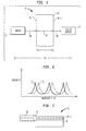
- an article of manufacture 10 e.g., a device, apparatus, subassembly, subsystem, system, etc.
- an optical path 11 defined by a source of radiation 12, a utilization device 14 and a transmission medium 18 coupling them to one another.
- a figure of merit (FOM) is defined for the optical path, and a body 16 of crystalline material is disposed in the path so that the FOM is satisfied.
- the crystalline material is highly transparent at a wavelength ⁇ of the radiation propagating in the path 11, and it has a coefficient of thermal expansion (CTE) and refractive index n such that the CTE and dn/dT are mutually adapted to satisfy the FOM over the range ⁇ T.
- CTE coefficient of thermal expansion
- n refractive index
- the source 12 may include an active device (e.g., a semiconductor laser) or a passive device (e.g., an optical waveguide through which an optical radiation signal propagates, or an object from which optical radiation is reflected or scattered), or a combination of active and passive devices.
- the utilization device 14 may include a photodetector, an optical receiver, an optical waveguide, an optical isolator, an optical coupler or multiplexor, a piece of terminal equipment, or a combination of them.
- the transmission medium 19 may include, for example, an air path, an optical fiber, or an integrated optical waveguide (as in the planar waveguides of silicon optical bench or semiconductor technology, for instance).
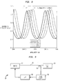
- a typical optical transmitter 90 that incorporates some of these components is illustrated in FIG. 9.
- a tunable source 92 is coupled to a utilization device 94 via an optical fiber 91.
- a portion of the laser output is tapped by coupler 93 to provide an input to frequency discriminator 96.
- the latter includes an etalon as the principal filtering element, as is well known in the art.
- the output of the frequency discriminator is provided to microprocessor 98 that generates an error signal to control the wavelength of source 92 (e.g., via its temperature and/or its drive current).
- the coupler, discriminator and microprocessor form a feedback loop that controls the source wavelength.
- This type of transmitter is described in more detail by D. A. Ackerman in copending, allowed patent application Serial No. 09/330, 389 filed on June 6, 1999. This application is assigned to the assignee hereof and is incorporated herein by reference.
- the article of manufacture 10 provides a frequency discrimination function; that is, the source 12 typically comprises a semiconductor laser, the utilization device 14 typically comprises a photodetector as part of an optical receiver, the transmission medium is air, and the body 16 of crystalline materials serves an etalon.
- an etalon includes essentially parallel input and output surfaces 16.1 and 16.2 that form a resonator of length L. Theses surfaces are typically coated so as to be partially transmissive and partially reflective to the radiation from source 12. When that radiation is coupled into the etalon through input surface 16.1, a standing wave pattern is formed as designated by the double-headed arrow 19.
- the transmission properties of the etalon are characterized by the well-recognized comb-like functions shown in FIG. 2.
- maximum transmission of radiation through the etalon occurs only at certain wavelengths that are spaced apart by c/2nL, where c is the speed of light in a vacuum, n is the group refractive index of the crystalline material of body 16, and L, in this case, is the separation of the surfaces as measured along the direction of radiation propagation therethrough. At wavelengths in between the maxima, the amount of radiation that is transmitted through the etalon decreases dramatically.
- the optical etalon operates to filter out signals at wavelengths other than those that are coincident, or nearly so, with the maxima in the etalon transmission characteristic, which may be used to stabilize the wavelength of the source 12.
- an etalon may be subjected to changes in temperature that cause the transmission characteristic to shift, as shown in FIG. 2.
- the curve labeled T 1 shifts to longer wavelengths (curve labeled T 2 ) when the temperature of the etalon increases from T 1 to T 2 .
- a decrease in temperature would cause the curves to shift to shorter wavelengths.
- Such changes in temperature could result from a variety of sources.
- the ambient temperature of the system in which the etalon is located could change due to natural causes (e.g., weather), or the temperature of the laser (which is often located in the same package as the etalon) could be changed intentionally as part of a wavelength tuning protocol (e.g., in a WDWM system), resulting in a change of the etalon's temperature, or the temperature control circuit could be imperfect due to its aging slowly or changing suddenly.
- temperature-induced shifts in the transmission characteristics of the etalon are undesirable inasmuch as significant shifts may cause the system performance to degrade to a level outside of system specifications.
- the change in optical path length through the etalon due to thermal expansion is balanced, or nearly so, by the temperature-induced change in its refractive index given by dn/dT; i.e., the etalon is made to be essentially temperature insensitive.
- L o nL
- the material should ideally have isotropic properties (e.g., an amorphous structure or a crystalline structure with cubic symmetry).
- isotropic properties e.g., an amorphous structure or a crystalline structure with cubic symmetry.
- the material to crystallize in a uniaxial crystal system (e.g., tetragonal, and hexagonal) in order to reduce the effects of birefringence on the radiation incident on the etalon from the source 12.
- a uniaxial crystal system e.g., tetragonal, and hexagonal
- uniaxial crystals with a relatively low FOM for the ordinary ray are oriented such that the principal axis is aligned with the propagation direction, in which case, polarization is not an issue.
- biaxial crystals and uniaxial crystals with a relative low FOM for the extraordinary ray are oriented such that the direction with preferred FOM is aligned with the propagation direction and a secondary axis is aligned with the polarization direction in order to reduce birefringence if the polarization of the source is known a priori (e.g., as with semiconductor lasers, which might be designed to be TE polarized).
- Suitable crystalline materials include LiCaAlF 6 and CaWO 4 , which are discussed in the Section entitled Crystalline Materials , infra .
- the crystal should preferably have no polarization dependence. For some applications, however, where the source generates polarized radiation, this constraint may be relaxed.
- thermo-optic behavior which includes the specific case of a temperature insensitive path.
- a specific requirement that is illustratively imposed on such an arrangement is that the temperature-induced change in the optical path length through the three materials be equal to the temperature-induced change in a cavity of length L 1 and material M1.
- FOM 3 -(n 2 L 2 /n 3 L 3 )FOM 2
- FOM 2 (n 2 L 2 ) -1 d/dT(n 2 L 2 )
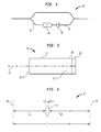
- FIG. 3 depicts an optical subsystem 50 including a semiconductor laser 52 (corresponding to material M1) coupled to a glass grating 56 (corresponding to material M2) via a compensating crystalline layer 54 (corresponding to material M3) disposed therebetween.
- a similar subsystem includes a compensating layer disposed between a silica waveguide (e.g. an integrated waveguide of the type used in silicon optical bench technology) and a garnet body (e.g., a Faraday rotator used in an optical isolator).
- a silica waveguide e.g. an integrated waveguide of the type used in silicon optical bench technology
- garnet body e.g., a Faraday rotator used in an optical isolator
- FIG. 4 depicts a Mach-Zender interferometer 40 including in one arm or branch a waveguide 42 (corresponding to material M1), a delay element 44 (corresponding to material M2), and a compensating layer 46 (corresponding to layer M3) disposed therebetween).
- a Mach-Zender interferometer 40 including in one arm or branch a waveguide 42 (corresponding to material M1), a delay element 44 (corresponding to material M2), and a compensating layer 46 (corresponding to layer M3) disposed therebetween).
- an alternative embodiment of our invention includes a folded optical path, as shown illustratively in FIG. 5.
- a portion of an optical path includes an optical waveguide 22, a thermo-optic compensating layer 26 of suitable crystalline material disposed at one end 22.1 of the waveguide 22, and a reflector 28 disposed on the compensating layer 26.
- An incoming radiation beam 21 from a source not shown is coupled into the other end 22.2 of the waveguide 22, propagates along the waveguide and through the compensating layer 26, and is reflected by the reflector 28 back into the layer 26 and then into the waveguide 22. The beam emerges from end 22.2.
- the optical path in a system or subsystem may include portions that constitute a free space path and in which a compensating material is disposed to cause the overall optical path to be temperature insensitive or to have some other desired thermo-optic behavior.
- a temperature insensitive optical path extending from one point fixed in space, through an optical element, to another point fixed in space, consider a telescope of the type illustrated in FIG. 6.
- a lens 36 is disposed between an object plane 32 and an image plane 34 that have a fixed separation.
- the lens 36 comprises a crystalline material in accordance with our invention.
- the following table illustrates the kind of crystalline materials that find utility in various embodiments of our invention depending on the specific application; e.g., depending on the wavelength of operation, the polarization conditions imposed by the components, and the degree of compensation desired.
- all of the materials listed in the table, except for PbS and ZnGeP 2 may be suitable for use in telecommunication systems operating at wavelengths in the range of about 1.2-1.7 ⁇ m, but those with FOMs in the approximate range of ⁇ 2 ppm/K are preferred for etalon applications; that is, AgCl, LiCaAlF 6 , LiIO 3 , CaCO 3 , and CaWO 4 are preferred.
- LiCaAlF 6 does not have the lowest FOM (in absolute value), yet it is currently preferred because it is stable, immune to water vapor, insensitive to light and relatively easy to process. LiCaAlF 6 has an FOM of -2.3 (calculated) and -1.55 (measured). All of the other materials in this group have smaller FOMs (in absolute value).
- the FOMs listed below have been calculated from data available in the literature. The data were taken for room temperature operation at visible wavelengths. However, we expect that the FOMs will not differ significantly at other temperatures within typical operating ranges (e.g., -40° C to +85° C) and that they are likely to improve at near infrared wavelengths. This predication is based, in part, on the recognition that for materials with band gap energies greater than about 1.5 eV dn/dT tends to be more sensitive to temperature and to wavelength as the latter approaches the ultraviolet and, conversely, less sensitive in the near infrared.
- a prior art etalon material (a-SiO 2 or fused silica) is included in the table.
- refractive index is intended to embrace both the simple index n of an essentially homogeneous, single layer body as well as the more complex effective index n eff of a multilayered and/or inhomogeneous body (e.g., a multi-layered waveguide).
Landscapes
- Physics & Mathematics (AREA)
- General Physics & Mathematics (AREA)
- Optics & Photonics (AREA)
- Nonlinear Science (AREA)
- Spectroscopy & Molecular Physics (AREA)
- Optical Integrated Circuits (AREA)
- Semiconductor Lasers (AREA)
- Optical Modulation, Optical Deflection, Nonlinear Optics, Optical Demodulation, Optical Logic Elements (AREA)
- Optical Filters (AREA)
- Lasers (AREA)
Abstract
Description
| Material | Orientation | n | dn/dT (ppm/K) | CTE (ppm/K) | CALC. FOM (ppm/K) |
| AgCl | isotropic | 2.002 | -61 | 31 | 0.5 |
| NaBr | isotropic | 1.615 | -30 | 42 | 23.4 |
| KBr | isotropic | 1.537 | -39 | 39 | 13.6 |
| CsBr | isotropic | 1.669 | -87 | 47 | -5.1 |
| NaCl | isotropic | 1.555 | -34 | 41 | 19.1 |
| KCl | isotropic | 1.475 | -36 | 36 | 11.6 |
| CsCl | isotropic | 1.620 | -77 | 45 | -2.5 |
| LiCaAlF6 | ordinary | 1.386 | -4.6 | 1.0 | -2.3 |
| LiSrAlF6 | ordinary | 1.401 | -4.0 | -9.0 | -11.9 |
| LiNbO3 | ordinary | 2.214 | 4.4 | 14.8 | 16.8 |
| LiIO3 | ordinary | 1.852 | -94 | 50 | -0.8 |
| CaCO3 | extraordinary | 1.480 | 10.5 | -5.8 | 1.3 |
| PbMoO4 | ordinary | 2.140 | -75 | 20 | -15.0 |
| CaMoO4 | ordinary | 1.945 | -9.6 | 12 | 17.1 |
| CaWO4 | ordinary | 1.898 | -10.2 | 6 | 0.6 |
| PbS | isotropic | 4.100 | -2100 | 19 | -493 |
| ZnGeP2 | ordinary | 3.167 | 151 - | 15.9 | 63.6 |
| Quartz SiO2 | ordinary | 1.542 | -5.5 | 7.1 | +3.5 |
| a-SiO2 | isotropic | 1.460 | 10.0 | 0.5 | 7.3 |
CaxPb1-xMoO4 (0 ≤ x ≤ 1) to be tailored to an FOM of zero as desired for etalon applications, or to any other FOM value between -15 and +17, as might be required by other applications. However, these materials crystallize in monoclinic structures (not uniaxial) and, therefore, should be utilized only for applications in which control of polarization is not important.
Claims (49)
- A method of controlling the thermo-optic behaviour of an optical path over a temperature range comprising the steps of:-determining a figure of merit (FOM) for the path; andincluding a body of crystalline material in the path, the material being highly transparent at a wavelength of radiation propagating in the path and having a coefficient of thermal expansion (CTE) and a refractive index change with temperature (dn/dT) that are mutually adapted to satisfy said FOM over said range.
- The method of claim 1 wherein said including step provides a crystalline material in which said CTE and dn/dT have the same signs.
- The method of claim 1 wherein said including step provides a crystalline material in which said CTE and dn/dT have opposite signs.
- The method of claim 3 wherein said including step provides a crystalline material that comprises LiRQF6, where R is selected from the group consisting of Ca and Sr or both, and Q is selected from the group consisting of Ga and A1 or both.
- The method of claim 4 wherein said including step provides a crystalline material that comprises LiCaA1F6.
- The method of claim 3 wherein said including step provides a crystalline material that comprises RCO3, where R is selected from the group consisting of Ca and Sr or both.
- The method of claim 6 wherein said including step provides a crystalline material that comprises CaCO3.
- The method of claim 3 wherein said including step provides a crystalline material that comprises RWO3, where R is selected from the group consisting of Ca and Sr or both.
- The method of claim 8 wherein said including step provides a crystalline material that comprises CaWO4.
- The method of claim 3 wherein said including step provides a crystalline material that comprises a halide of K, Cs or both.
- The method of claim 3 wherein said including step provides a crystalline material that comprises a molybdate.
- The method of claim 11 wherein said molybdate is selected from the group consisting of PbMoO4 and CaMoO4.
- The method of claim 1 wherein said optical path is defined by a temperature insensitive etalon, and said FOM is determined to be CTE = -(1/n)(dn/dT), where n is the refractive index of the crystalline material of said etalon.
- The method of claim 13 wherein dn/dT is relatively insensitive to temperature and wavelength over the operating range of interest.
- The method of claim 13 wherein said material is selected from the group consisting of AgC1, LiCaA1F6, LilO3, CaCO3 and CaWO4.
- The method of claim 1 wherein said optical path is defined by the object and image planes of a telescope that have a fixed separation and a lens located therebetween, and said FOM is determined to be (n-1)CTE = -dn/dT, where n is the refractive index of the crystalline material of said lens and CTE is the coefficient of thermal expansion of the crystalline material of said lens.
- The method of claim 1 wherein said optical path is a folded path at at least one location thereof and said including step comprises positioning said body at said location.
- The method of claim 1 wherein said optical path includes first, second and third portions having lengths L1, L2 and L3 and refractive indices n1, n2 and n3, respectively.
- The method of claim 18 wherein said third portion is disposed between said first and second portions and comprises said body, and said FOM is determined to be FOM3 = -(n2L2/n3L3)FOM2.
- The method of claim 19 wherein said first portion comprises a glass waveguide and said second portion comprises a crystalline device.
- The method of claim 18 wherein said optical path comprises an arm of a Mach-Zender interferometer, said first portion comprising a delay element in said arm, said second portion comprising an optical waveguide in said arm, and said third portion comprising said body.
- An article of manufacture comprising:-an optical path characterised by a figure of merit (FOM); anda body of crystalline material disposed in said path, said material being highly transparent at a wavelength of radiation propagating in the path and having a coefficient of thermal expansion (CTE) and a refractive index change with temperature (dn/dT) that are mutually adapted to satisfy said FOM over a range of temperatures.
- The article of claim 22 wherein said body comprises a crystalline material in which said CTE and dn/dT have the same signs.
- The article of claim 22 wherein said body comprises a crystalline material in which said CTE and dn/dT have opposite signs.
- The article of claim 24 wherein said crystalline material that comprises LiRQF6, where R is selected from the group consisting of Ca and Sr or both and Q is selected from the group consisting of Ga and A1 or both.
- The article of claim 25 wherein said crystalline material that comprises LiCaA1F6.
- The article of claim 24 wherein said crystalline material that comprises RCO3, where R is selected from the group consisting of Ca and Sr or both.
- The article of claim 27 wherein said crystalline material that comprises CaCO3.
- The article of claim 24 wherein said crystalline material that comprises RWO3, where R is selected from the group consisting of Ca and Sr or both.
- The article of claim 28 wherein said crystalline material that comprises CaWO3.
- The article of claim 24 wherein said crystalline material comprises a halide of K, Cs or both.
- The article of claim 24 wherein said crystalline material comprises a molybdate.
- The article of claim 32 wherein said molybdate is selected from the group consisting of PbMoO4 and CaMoO4.
- The article of claim 22 wherein said optical path is defined by a temperature insensitive etalon, and said FOM is defined by the equation CTE = -(1/n)(dn/dT), where n is the refractive index of the crystalline material of said etalon.
- The article of claim 34 wherein dn/dT is relatively insensitive to temperature and wavelength over the operating range of interest.
- The article of claim 34 wherein said material is selected from the group consisting of AgC1, LiCaA1F6, LilO3, CaCO3 and CaWO4.
- The article of claim 22 wherein said optical path is defined by the object and image planes of a telescope that have a fixed separation and a lens located therebetween, and said FOM is defined by the equation (n-1)CTE= -dn/dT, where n is the refractive index of the crystalline material of said lens and CTE is the coefficient of thermal expansion of the crystalline material of said lens.
- The article of claim 22 wherein said optical path is a folded path at at least one location thereof, said body being disposed at said location.
- The article of claim 22 wherein said optical path includes first, second and third portions having lengths L1, L2 and L3 and refractive indices n1, n2 and n3, respectively.
- The article of claim 39 wherein said third portion is disposed between said first and second portions and comprises said body, and said FOM is defined by the equation FOM3 = (n2L2/n3L3) FOM2.
- The article of claim 40 wherein said first portion comprises a glass waveguide and said second portion comprises a crystalline device.
- The article of claim 39 wherein said optical path comprises an arm of a Mach-Zender interferometer, said first portion comprising a delay element in said arm, said second portion comprising an optical waveguide in said arm, and said third portion comprising said body.
- The article of claim 22 wherein said optical path is included in a temperature sensor and said crystalline material comprises PbS.
- A WDM optical transmitter for operation over a range of temperatures comprising:-a source for generating an output signal at any one of a multiplicity of different wavelengths;a temperature controller for tuning the wavelength of said source to a predetermined one of said wavelengths; anda feedback loop including a frequency discriminator for stabilising the wavelength of said source at said predetermined wavelength, said discriminator including an etalon, characterised in that:-said etalon has a FOM; andsaid etalon comprises a body of crystalline material that is highly transparent to radiation at said predetermined wavelength and that has a CTE and a dn/dT that are mutually adapted to satisfy said FOM over said temperature range.
- The WDM optical transmitter of claim 44 wherein said FOM = CTE + (1 /n)(dn/dT).
- The WDM optical transmitter of claim 45 wherein dn/dT is relatively insensitive to temperature and wavelength over the operating range of interest.
- The WDM optical transmitter of claim 46 wherein said etalon is essentially temperature insensitive and said FOM is essentially zero.
- The WDM optical transmitter of claim 47 wherein said crystalline material comprises LiRQF6, where R is selected from the group consisting of Ca and Sr or both and Q is selected from the group consisting of Ga and A1 or both.
- The WDM optical transmitter of claim 48 wherein said material comprises LiCaA1F6.
Applications Claiming Priority (2)
| Application Number | Priority Date | Filing Date | Title |
|---|---|---|---|
| US525512 | 1983-08-22 | ||
| US09/525,512 US6486999B1 (en) | 2000-03-15 | 2000-03-15 | Using crystalline materials to control the thermo-optic behavior of an optical path |
Publications (2)
| Publication Number | Publication Date |
|---|---|
| EP1136848A2 true EP1136848A2 (en) | 2001-09-26 |
| EP1136848A3 EP1136848A3 (en) | 2003-05-21 |
Family
ID=24093559
Family Applications (1)
| Application Number | Title | Priority Date | Filing Date |
|---|---|---|---|
| EP01302416A Withdrawn EP1136848A3 (en) | 2000-03-15 | 2001-03-15 | Using crystalline materials to control the thermo-optic behaviour of an optical path |
Country Status (5)
| Country | Link |
|---|---|
| US (1) | US6486999B1 (en) |
| EP (1) | EP1136848A3 (en) |
| JP (1) | JP4018344B2 (en) |
| CN (1) | CN1313522A (en) |
| CA (1) | CA2336492A1 (en) |
Cited By (2)
| Publication number | Priority date | Publication date | Assignee | Title |
|---|---|---|---|---|
| WO2003087898A1 (en) * | 2002-04-15 | 2003-10-23 | Mitsubishi Denki Kabushiki Kaisha | Wavelength filter and wavelength monitoring apparatus |
| EP1304777B1 (en) * | 2001-09-28 | 2007-07-25 | The Furukawa Electric Co., Ltd. | Optical filter, laser module, and wavelength locker module |
Families Citing this family (19)
| Publication number | Priority date | Publication date | Assignee | Title |
|---|---|---|---|---|
| US6278549B1 (en) * | 2000-04-17 | 2001-08-21 | Ciena Corporation | Optical filter having a quartz substrate |
| WO2002091534A1 (en) * | 2001-05-08 | 2002-11-14 | Mitsubishi Denki Kabushiki Kaisha | Wavelength monitoring apparatus |
| US7016097B2 (en) * | 2002-01-07 | 2006-03-21 | Triquint Technology Holding Co. | Optical device with a temperature insensitive optical pathlength |
| US20040001258A1 (en) * | 2002-06-28 | 2004-01-01 | Mandeep Singh | Solid state etalons with low thermally-induced optical path length change |
| KR100496986B1 (en) * | 2002-11-01 | 2005-06-28 | 한국전자통신연구원 | Wavelength Revision Method for Wavelength Shift |
| US7058099B2 (en) * | 2002-11-08 | 2006-06-06 | Finisar Corporation | Age compensation in optoelectronic modules with integrated temperature control |
| EP1605284B1 (en) * | 2003-03-19 | 2012-12-26 | Mitsubishi Denki Kabushiki Kaisha | Wavelength filter and wavelength monitor device |
| JP2005003806A (en) | 2003-06-10 | 2005-01-06 | Sun Tec Kk | Optical element, wavelength tunable optical filter, and optical add / drop module |
| JP2005037762A (en) | 2003-07-17 | 2005-02-10 | Sun Tec Kk | Optical element, wavelength tunable optical filter, optical add / drop module, and wavelength tunable light source |
| JP4084360B2 (en) * | 2004-03-31 | 2008-04-30 | 株式会社東芝 | Optical frequency stabilization device and optical frequency stabilization method |
| US7525604B2 (en) * | 2005-03-15 | 2009-04-28 | Naxellent, Llc | Windows with electrically controllable transmission and reflection |
| US7973998B2 (en) * | 2007-05-18 | 2011-07-05 | Serious Materials, Inc. | Temperature activated optical films |
| CN101775655B (en) * | 2010-01-13 | 2013-07-17 | 福州高意通讯有限公司 | Laser crystal and preparation method thereof |
| US9036109B2 (en) | 2012-08-20 | 2015-05-19 | Apple Inc. | Electronic device with thermally matched light guide plate |
| CN103116217B (en) * | 2013-03-18 | 2016-12-28 | 上海浦芮斯光电科技有限公司 | A kind of adjustable etalon of wide wavelength range |
| JP2015081316A (en) * | 2013-10-24 | 2015-04-27 | 株式会社トクヤマ | Inorganic particle filled silicone resin composition |
| CN104062096B (en) * | 2014-06-27 | 2017-01-04 | 哈尔滨工业大学深圳研究生院 | A kind of method that crystal optical index is affected by voltage compensation temperature |
| CN117111235B (en) * | 2023-10-17 | 2023-12-19 | 成都光创联科技有限公司 | Compensation system, manufacturing and compensation method for high-low temperature power drop of optical device |
| CN120149932A (en) * | 2025-03-14 | 2025-06-13 | 中国科学院理化技术研究所 | Laser device and laser amplifier |
Family Cites Families (14)
| Publication number | Priority date | Publication date | Assignee | Title |
|---|---|---|---|---|
| US4497544A (en) * | 1982-12-27 | 1985-02-05 | Honeywell Inc. | Optical imaging device and method |
| US4615587A (en) * | 1983-01-06 | 1986-10-07 | Ltv Aerospace And Defense Company | High speed erasing and rebiasing of thermoptic thin films |
| JPS59163529A (en) * | 1983-03-09 | 1984-09-14 | Agency Of Ind Science & Technol | Light-applied temperature measuring device |
| US4886331A (en) * | 1988-03-17 | 1989-12-12 | Environmental Research Institute Of Michigan | Thermo-optically induced waveguide |
| US5212584A (en) * | 1992-04-29 | 1993-05-18 | At&T Bell Laboratories | Tunable etalon filter |
| US5202939A (en) * | 1992-07-21 | 1993-04-13 | Institut National D'optique | Fabry-perot optical sensing device for measuring a physical parameter |
| CA2101411C (en) * | 1992-08-14 | 2003-06-10 | Jean-Pierre Weber | Tunable optical filter |
| US5608568A (en) * | 1994-04-11 | 1997-03-04 | The Johns Hopkins University | Thin film vanadium oxide spatial light modulators and methods |
| JP3294986B2 (en) * | 1996-03-22 | 2002-06-24 | 富士通株式会社 | Optical element without temperature dependence |
| US5938811A (en) * | 1997-05-23 | 1999-08-17 | Lucent Technologies Inc. | Method for altering the temperature dependence of optical waveguides devices |
| US6370169B1 (en) * | 1998-04-22 | 2002-04-09 | Nippon Telegraph & Telephone Corporation | Method and apparatus for controlling optical wavelength based on optical frequency pulling |
| JP2000091681A (en) * | 1998-09-09 | 2000-03-31 | Japan Atom Energy Res Inst | Long-distance laser light propagation in a medium by controlling the wavefront |
| DE19923061A1 (en) * | 1999-05-20 | 2000-11-23 | Bosch Gmbh Robert | Thermo-optical modulator |
| US6384958B1 (en) * | 2000-06-26 | 2002-05-07 | Jds Uniphase Corporation | Free-space thermo-optical devices |
-
2000
- 2000-03-15 US US09/525,512 patent/US6486999B1/en not_active Expired - Lifetime
-
2001
- 2001-03-01 CA CA002336492A patent/CA2336492A1/en not_active Abandoned
- 2001-03-14 CN CN01111367A patent/CN1313522A/en active Pending
- 2001-03-15 JP JP2001073540A patent/JP4018344B2/en not_active Expired - Fee Related
- 2001-03-15 EP EP01302416A patent/EP1136848A3/en not_active Withdrawn
Cited By (2)
| Publication number | Priority date | Publication date | Assignee | Title |
|---|---|---|---|---|
| EP1304777B1 (en) * | 2001-09-28 | 2007-07-25 | The Furukawa Electric Co., Ltd. | Optical filter, laser module, and wavelength locker module |
| WO2003087898A1 (en) * | 2002-04-15 | 2003-10-23 | Mitsubishi Denki Kabushiki Kaisha | Wavelength filter and wavelength monitoring apparatus |
Also Published As
| Publication number | Publication date |
|---|---|
| US6486999B1 (en) | 2002-11-26 |
| CN1313522A (en) | 2001-09-19 |
| JP2001324702A (en) | 2001-11-22 |
| CA2336492A1 (en) | 2001-09-15 |
| EP1136848A3 (en) | 2003-05-21 |
| JP4018344B2 (en) | 2007-12-05 |
Similar Documents
| Publication | Publication Date | Title |
|---|---|---|
| US6486999B1 (en) | Using crystalline materials to control the thermo-optic behavior of an optical path | |
| US20040001258A1 (en) | Solid state etalons with low thermally-induced optical path length change | |
| US5212584A (en) | Tunable etalon filter | |
| US7221827B2 (en) | Tunable dispersion compensator | |
| EP3065237B1 (en) | A temperature insensitive laser | |
| US20030076505A1 (en) | Cascaded fiber fabry-perot filters | |
| US20030012250A1 (en) | Tunable filter for laser wavelength selection | |
| US8456741B2 (en) | Optical module having three or more optically transparent layers | |
| Sakurai et al. | Control of group delay and chromatic dispersion in tunable hollow waveguide with highly reflective mirrors | |
| EP1304777B1 (en) | Optical filter, laser module, and wavelength locker module | |
| EP1197764A2 (en) | Strain-stabilized birefringent crystal | |
| Torner et al. | New type of guided waves in birefringent media | |
| US6452725B1 (en) | Thermally stable etalon wavelength interleaver-multiplexer | |
| JP3291915B2 (en) | Optical filter and oscillation wavelength stabilized light source | |
| JP3404031B2 (en) | Integrated optical multiplexer / demultiplexer | |
| CN1759331B (en) | Wavelength filter and wavelength monitoring device | |
| CN113365032A (en) | Temperature compensation etalon and adjustable laser packaging structure | |
| Magden et al. | Laser frequency stabilization using Pound-Drever-Hall technique with an integrated TiO2 athermal resonator | |
| Chung | Temperature-tuned ZnS etalon filters for WDM systems | |
| JP4214808B2 (en) | Optical component, optical apparatus, and optical communication system | |
| US7016097B2 (en) | Optical device with a temperature insensitive optical pathlength | |
| KR100400890B1 (en) | Variable optical attenuator of in-line type and fabrication method thereof | |
| EP1536273A1 (en) | Polarization-independent electro-optic modulator | |
| JPH1062625A (en) | Wavelength filter | |
| Shirasaki | Temperature insensitive design of Fabry-Perot etalon |
Legal Events
| Date | Code | Title | Description |
|---|---|---|---|
| PUAI | Public reference made under article 153(3) epc to a published international application that has entered the european phase |
Free format text: ORIGINAL CODE: 0009012 |
|
| AK | Designated contracting states |
Kind code of ref document: A2 Designated state(s): AT BE CH CY DE DK ES FI FR GB GR IE IT LI LU MC NL PT SE TR |
|
| AX | Request for extension of the european patent |
Free format text: AL;LT;LV;MK;RO;SI |
|
| PUAL | Search report despatched |
Free format text: ORIGINAL CODE: 0009013 |
|
| AK | Designated contracting states |
Designated state(s): AT BE CH CY DE DK ES FI FR GB GR IE IT LI LU MC NL PT SE TR |
|
| AX | Request for extension of the european patent |
Extension state: AL LT LV MK RO SI |
|
| AKX | Designation fees paid | ||
| REG | Reference to a national code |
Ref country code: DE Ref legal event code: 8566 |
|
| STAA | Information on the status of an ep patent application or granted ep patent |
Free format text: STATUS: THE APPLICATION IS DEEMED TO BE WITHDRAWN |
|
| 18D | Application deemed to be withdrawn |
Effective date: 20031122 |