EP1134894A2 - Improvements in or relating to digital-to-analog converters - Google Patents
Improvements in or relating to digital-to-analog converters Download PDFInfo
- Publication number
- EP1134894A2 EP1134894A2 EP01200726A EP01200726A EP1134894A2 EP 1134894 A2 EP1134894 A2 EP 1134894A2 EP 01200726 A EP01200726 A EP 01200726A EP 01200726 A EP01200726 A EP 01200726A EP 1134894 A2 EP1134894 A2 EP 1134894A2
- Authority
- EP
- European Patent Office
- Prior art keywords
- inverter
- transistor
- pull
- coupled
- node
- Prior art date
- Legal status (The legal status is an assumption and is not a legal conclusion. Google has not performed a legal analysis and makes no representation as to the accuracy of the status listed.)
- Withdrawn
Links
Images

Classifications
-
- H—ELECTRICITY
- H03—ELECTRONIC CIRCUITRY
- H03K—PULSE TECHNIQUE
- H03K17/00—Electronic switching or gating, i.e. not by contact-making and –breaking
- H03K17/04—Modifications for accelerating switching
- H03K17/041—Modifications for accelerating switching without feedback from the output circuit to the control circuit
- H03K17/04106—Modifications for accelerating switching without feedback from the output circuit to the control circuit in field-effect transistor switches
-
- H—ELECTRICITY
- H03—ELECTRONIC CIRCUITRY
- H03K—PULSE TECHNIQUE
- H03K17/00—Electronic switching or gating, i.e. not by contact-making and –breaking
- H03K17/51—Electronic switching or gating, i.e. not by contact-making and –breaking characterised by the components used
- H03K17/56—Electronic switching or gating, i.e. not by contact-making and –breaking characterised by the components used by the use, as active elements, of semiconductor devices
- H03K17/687—Electronic switching or gating, i.e. not by contact-making and –breaking characterised by the components used by the use, as active elements, of semiconductor devices the devices being field-effect transistors
- H03K17/693—Switching arrangements with several input- or output-terminals, e.g. multiplexers, distributors
Definitions
- This invention generally relates to electronic systems and in particular it relates to differential switching schemes for current-mode digital-to-analog converters (DACs).
- DACs digital-to-analog converters
- Digital-to-analog converters mainly designed for video applications have a very poor spectral purity when used in communication applications such as the transmit portion of wired and/or wireless digital communication systems.
- Delay differences between when a bit turns on and when it turns off results in a shift from the ideal fifty percent duty cycle (square wave) and leads to even-order harmonics in the output spectrum.
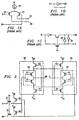
- a typical prior art CMOS current-mode DAC switching scheme shown in Figure 1A, includes transistors 20 and 22; current source 24; input nodes Q and QB; and output nodes 26 and 28.
- the time skew between Q and QB is of major concern for communication applications.
- the switches (transistors) 20 and 22 are like a differential pair.
- the prior art circuit of Figure 1 uses PMOS transistors, but the same problems with time skew also exist when NMOS switches and current sources are used.
- the differential switching circuit includes: a first inverter; a first pull-up transistor coupled between the first inverter and a high-side power supply node; a first pull-down transistor coupled between the first inverter and a low-side power supply node; an output node of the first inverter coupled to a control node of the first pull-up transistor and a control node of the first pull-down transistor; a second inverter; a second pull-up transistor coupled between the second inverter and the high-side power supply node; a second pull-down transistor coupled between the second inverter and the low-side power supply node; and an output node of the second inverter coupled to a control node of the second pull-up transistor and a control node of the second pull-down transistor, wherein the first and second inverters are coupled together between the inverters and the pull-up transistors, and between the inverters and the pull-down transistors.
- FIG. 2 A preferred embodiment skewless differential switching circuit is shown in Figure 2.
- the circuit of Figure 2 includes NMOS transistors 32-37; PMOS transistors 40-45; digital input data D and DB; switch control data Q and QB; clock signal CK; and source voltages V DD and V SS .
- Transistors 35 and 42 form inverter 46.
- Transistors 37 and 44 form inverter 47.
- Inverter 46 and transistors 34 and 43 form skewless switching element 48.
- Inverter 47 and transistors 36 and 45 form skewless switching element 49.
- Transistors 40 and 41 serve as digital data storage elements. This circuit provides a switching scheme that minimizes the time skew between Q and QB.
- This switching scheme not only gives a minimum possible time-skew, but, also, gives the same rise and fall times. Equal rise and fall times is very essential when a DAC is reconstructing a sine wave. For minimum harmonic distortion, both half-cycles of the sinusoidal waveform need to have the same rise and fall characteristics.
- D and DB are the complementary signals with skew, while Q and QB are their respective final skewless outputs.
- both control signals by design are forced to wait for each other before moving on to control one of the two switches.
- the path of Q to its final level is controlled by QB, while at the same time, Q controls the path of QB to its final voltage level.
- the only way for D to reach the switch is if and only if QB allows Q to do so
- the only way for DB to reach the other switch is if and only if Q allows QB to do so.
- the circuit of Figure 2 operates as follows.
- the digital data D and DB is allowed to settle and take its final value before clock signal CK goes high and turns on the pass transistors (switches) 32 and 33.
- NMOS transistors 32 and 33 pass bad ONES (voltage levels not high enough to be detected as a ONE)
- pull up transistors (switches) 40 and 41 are used to restore the voltage level to V DD .
- transistors 20 and 21, shown in Figure 1 form a differential pair, Q and QB do not need to swing to V DD and V SS .
- a diode-connected PMOS transistor 50 is added between V DD and transistor 43, and a diode-connected PMOS transistor 52 is added between V DD and transistor 45, as shown in the circuit of Figure 3.
- a diode-connected NMOS transistor 54 is added between V SS and transistor 34, and a diode connected NMOS transistor 56 is added between V SS and transistor 36, as shown in Figure 3.
- the skewless differential DAC switch driver is used as shown in Figures 4 and 5.
- the circuit of Figure 4 includes PMOS transistors 60 and 62; DAC load resistances 64 and 66; switch driver 68; and current source 70.
- the circuit of Figure 5 includes NMOS transistors 74 and 76; DAC load resistances 78 and 80; switch driver 82; and current source 84.
- the circuit of Figure 4 uses PMOS transistors and the circuit of Figure 5 uses NMOS transistors. D and DB are provided by DAC logic circuitry and are assumed to have settled to their final state.
- the preferred embodiment provides several advantages. Skew reduction is guaranteed by design because Q waits for QB to become valid, while at the same time, QB waits for Q to become valid before allowing either one of them to go to the differential switch. This circuit works well for a wide supply range such as 2.7 to 5.0 volts. Unlike the prior art solution of U.S. Patent 5,689,257, there is no reduction in performance from the additional skew introduced between D and DB by NMOS pass transistors 32 and 33 as they pass a good ZERO, but a bad ONE. If needed, instead of using the simple pull-up PMOS transistors 40 and 41, a variety of different types of storage elements, such as cross-coupled inverters, can be used. The preferred embodiment is not limited by the mismatches between the two identical cross-coupled inverters used for minimizing the skew in U.S. Patent 5,689,257.
Landscapes
- Logic Circuits (AREA)
- Amplifiers (AREA)
- Analogue/Digital Conversion (AREA)
- Electronic Switches (AREA)
Abstract
Description
Claims (10)
- A differential switching circuit comprising:a first pull-up transistor coupled between a first inverter and a high-side power supply node;a first pull-down transistor coupled between the first inverter and a low-side power supply node;an output node of the first inverter coupled to a control node of the first pull-up transistor and a control node of the first pull-down transistor;a second pull-up transistor coupled between a second inverter and the high-side power supply node;a second pull-down transistor coupled between the second inverter and the low-side power supply node; andan output node of the second inverter coupled to a control node of the second pull-up transistor and a control node of the second pull-down transistor, wherein the first and second inverters are coupled together between the inverters and the pull-up transistors, and between the inverters and the pull-down transistors.
- The circuit of claim 1 further comprising:a first transfer switch coupled to an input of the first inverter; anda second transfer switch coupled to an input of the second inverter.
- The circuit of claim 2 further comprising:a first storage element coupled to the input of the first inverter; anda second storage element coupled to the input of the second inverter.
- The circuit of claim 3 wherein the first storage element is a first transistor coupled between the input of the first inverter and the high side power supply node; and the second storage element is a second transistor coupled between the input of the second inverter and the high side power supply node.
- The circuit of claim 4 wherein a control node of the first transistor is coupled to the input of the second inverter; and a control node of the second transistor is coupled to the input of the first inverter.
- The circuit of any of claims 2 to 5 wherein the first and second transfer switches are transistors.
- The circuit of any of claims 2 to 5 wherein the first and second transfer switches are NMOS transistors.
- The circuit of any preceding claim further comprising:
a current mode digital-to-analog converter switching circuit coupled to the output node of the first inverter and the output node of the second inverter. - The circuit of claim 8 wherein the converter switching circuit comprises:a first transistor coupled to a current source, a control node of the first transistor coupled to the output of the first inverter; anda second transistor coupled to the current source, a control node of the second transistor coupled to the output of the second inverter.
- A digital-to-analog converter comprising:a first pull-up transistor coupled between a first inverter and a high-side power supply node;a first pull-down transistor coupled between the first inverter and a low-side power supply node;an output node of the first inverter coupled to a control node of the first pull-up transistor and a control node of the first pull-down transistor;a second pull-up transistor coupled between a second inverter and the high-side power supply node;a second pull-down transistor coupled between the second inverter and the low-side power supply node;an output node of the second inverter coupled to a control node of the second pull-up transistor and a control node of the second pull-down transistor, wherein the first and second inverters are coupled together between the inverters and the pull-up transistors, and between the inverters and the pull-down transistors; anda current mode digital-to-analog converter switching circuit coupled to the output node of the first inverter and the output node of the second inverter.
Applications Claiming Priority (2)
| Application Number | Priority Date | Filing Date | Title |
|---|---|---|---|
| US18499500P | 2000-02-25 | 2000-02-25 | |
| US184995P | 2000-02-25 |
Publications (2)
| Publication Number | Publication Date |
|---|---|
| EP1134894A2 true EP1134894A2 (en) | 2001-09-19 |
| EP1134894A3 EP1134894A3 (en) | 2003-11-19 |
Family
ID=22679114
Family Applications (1)
| Application Number | Title | Priority Date | Filing Date |
|---|---|---|---|
| EP01200726A Withdrawn EP1134894A3 (en) | 2000-02-25 | 2001-02-26 | Improvements in or relating to digital-to-analog converters |
Country Status (2)
| Country | Link |
|---|---|
| EP (1) | EP1134894A3 (en) |
| JP (1) | JP2001298351A (en) |
Cited By (1)
| Publication number | Priority date | Publication date | Assignee | Title |
|---|---|---|---|---|
| WO2008116206A1 (en) * | 2007-03-21 | 2008-09-25 | Qualcomm Incorporated | Circuit device and method of controlling a voltage swing |
Families Citing this family (2)
| Publication number | Priority date | Publication date | Assignee | Title |
|---|---|---|---|---|
| KR100430369B1 (en) * | 2002-05-03 | 2004-05-04 | (주) 텔트론 | RF Differential Switch Circuit |
| KR100831359B1 (en) | 2003-01-23 | 2008-05-21 | 삼성전자주식회사 | Low skew and glitch digital analog inverter |
Family Cites Families (4)
| Publication number | Priority date | Publication date | Assignee | Title |
|---|---|---|---|---|
| DE58908782D1 (en) * | 1989-09-22 | 1995-01-26 | Itt Ind Gmbh Deutsche | Two phase clock generator. |
| JP2947042B2 (en) * | 1993-12-28 | 1999-09-13 | 日本電気株式会社 | Low phase difference differential buffer |
| GB9404013D0 (en) * | 1994-03-02 | 1994-04-20 | Inmos Ltd | Current generating unit |
| GB2333191A (en) * | 1998-01-08 | 1999-07-14 | Fujitsu Microelectronics Ltd | DAC current switch with reduced crossover noise |
-
2001
- 2001-02-21 JP JP2001044864A patent/JP2001298351A/en active Pending
- 2001-02-26 EP EP01200726A patent/EP1134894A3/en not_active Withdrawn
Cited By (5)
| Publication number | Priority date | Publication date | Assignee | Title |
|---|---|---|---|---|
| WO2008116206A1 (en) * | 2007-03-21 | 2008-09-25 | Qualcomm Incorporated | Circuit device and method of controlling a voltage swing |
| US7567096B2 (en) | 2007-03-21 | 2009-07-28 | Qualcomm Incorporated | Circuit device and method of controlling a voltage swing |
| JP2010522522A (en) * | 2007-03-21 | 2010-07-01 | クゥアルコム・インコーポレイテッド | Circuit device and method for controlling voltage swing |
| RU2406220C1 (en) * | 2007-03-21 | 2010-12-10 | Квэлкомм Инкорпорейтед | Circuit arrangement and voltage swing control method |
| JP2013232209A (en) * | 2007-03-21 | 2013-11-14 | Qualcomm Inc | Circuit device and method of controlling voltage swing |
Also Published As
| Publication number | Publication date |
|---|---|
| EP1134894A3 (en) | 2003-11-19 |
| JP2001298351A (en) | 2001-10-26 |
Similar Documents
| Publication | Publication Date | Title |
|---|---|---|
| EP0935345B1 (en) | Differential switching circuitry | |
| US5969542A (en) | High speed gate oxide protected level shifter | |
| JP3689197B2 (en) | Level shift circuit | |
| US9048864B2 (en) | Digital to analog converter with current steering source for reduced glitch energy error | |
| US6020768A (en) | CMOS low-voltage comparator | |
| US5103116A (en) | CMOS single phase registers | |
| EP1326342B1 (en) | Level shift circuit for transmitting signal from leading edge to trailing edge of input signal | |
| JP2993395B2 (en) | Level shift circuit | |
| US20210005231A1 (en) | Latching sense amplifier | |
| EP2965425A1 (en) | Voltage level shifter with a low-latency voltage boost circuit | |
| WO1994024764A1 (en) | Ecl and ttl to cmos logic converter | |
| JP4691013B2 (en) | Signal processing circuit and method | |
| US20110037511A1 (en) | Multiple signal switching circuit, current switching cell circuit, latch circuit, current steering type dac, semiconductor integrated circuit, video device, and communication device | |
| US6310569B1 (en) | Skewless differential switching scheme for current-mode digital-to-analog converters | |
| KR100316428B1 (en) | Voltage selector for a d/a converter | |
| US7629814B2 (en) | Latch circuit and deserializer circuit | |
| TWI660585B (en) | Latch circuit | |
| US7973681B2 (en) | High speed, low power non-return-to-zero/return-to-zero output driver | |
| US6794907B2 (en) | Low jitter high speed CMOS to CML clock converter | |
| CN121124817A (en) | A current-controlled digital-to-analog converter for capacitively coupled transmission of switch control signals | |
| US6294940B1 (en) | Symmetric clock receiver for differential input signals | |
| US10771077B1 (en) | Hybrid return-to-zero voltage-mode DAC driver | |
| KR102478261B1 (en) | Low-power and high speed transceiver using di-code signaling and calibration method thereof | |
| JP2001298351A (en) | Skewless differential switching configuration for current mode digital-to-analog converter | |
| US7199742B2 (en) | Digital-to-analog converter and related level shifter thereof |
Legal Events
| Date | Code | Title | Description |
|---|---|---|---|
| PUAI | Public reference made under article 153(3) epc to a published international application that has entered the european phase |
Free format text: ORIGINAL CODE: 0009012 |
|
| 17P | Request for examination filed |
Effective date: 20010226 |
|
| AK | Designated contracting states |
Kind code of ref document: A2 Designated state(s): AT BE CH CY DE DK ES FI FR GB GR IE IT LI LU MC NL PT SE TR |
|
| AX | Request for extension of the european patent |
Free format text: AL;LT;LV;MK;RO;SI |
|
| PUAL | Search report despatched |
Free format text: ORIGINAL CODE: 0009013 |
|
| AK | Designated contracting states |
Kind code of ref document: A3 Designated state(s): AT BE CH CY DE DK ES FI FR GB GR IE IT LI LU MC NL PT SE TR |
|
| AX | Request for extension of the european patent |
Extension state: AL LT LV MK RO SI |
|
| AKX | Designation fees paid |
Designated state(s): AT BE CH CY DE DK ES FI FR GB GR IE IT LI LU MC NL PT SE TR |
|
| STAA | Information on the status of an ep patent application or granted ep patent |
Free format text: STATUS: THE APPLICATION IS DEEMED TO BE WITHDRAWN |
|
| 18D | Application deemed to be withdrawn |
Effective date: 20040520 |