EP1134859A1 - Dispositif d'amplification optique - Google Patents
Dispositif d'amplification optique Download PDFInfo
- Publication number
- EP1134859A1 EP1134859A1 EP01400465A EP01400465A EP1134859A1 EP 1134859 A1 EP1134859 A1 EP 1134859A1 EP 01400465 A EP01400465 A EP 01400465A EP 01400465 A EP01400465 A EP 01400465A EP 1134859 A1 EP1134859 A1 EP 1134859A1
- Authority
- EP
- European Patent Office
- Prior art keywords
- optical
- signal
- wave
- modulation
- compensation
- Prior art date
- Legal status (The legal status is an assumption and is not a legal conclusion. Google has not performed a legal analysis and makes no representation as to the accuracy of the status listed.)
- Granted
Links
- 230000003287 optical effect Effects 0.000 title claims abstract description 101
- 239000004065 semiconductor Substances 0.000 claims abstract description 16
- 230000002238 attenuated effect Effects 0.000 claims abstract description 5
- 230000008878 coupling Effects 0.000 claims abstract description 5
- 238000010168 coupling process Methods 0.000 claims abstract description 5
- 238000005859 coupling reaction Methods 0.000 claims abstract description 5
- 230000003321 amplification Effects 0.000 claims description 8
- 238000003199 nucleic acid amplification method Methods 0.000 claims description 8
- 230000002441 reversible effect Effects 0.000 claims description 5
- 230000000295 complement effect Effects 0.000 claims description 4
- 239000000463 material Substances 0.000 claims description 3
- 230000005540 biological transmission Effects 0.000 abstract description 6
- 238000010586 diagram Methods 0.000 description 12
- 230000004044 response Effects 0.000 description 8
- 230000008901 benefit Effects 0.000 description 4
- 230000008033 biological extinction Effects 0.000 description 4
- 230000007423 decrease Effects 0.000 description 3
- 239000000969 carrier Substances 0.000 description 2
- 239000000835 fiber Substances 0.000 description 2
- 230000010287 polarization Effects 0.000 description 2
- 230000001360 synchronised effect Effects 0.000 description 2
- 229910052691 Erbium Inorganic materials 0.000 description 1
- 238000010521 absorption reaction Methods 0.000 description 1
- 230000009286 beneficial effect Effects 0.000 description 1
- 230000015556 catabolic process Effects 0.000 description 1
- 238000006243 chemical reaction Methods 0.000 description 1
- 230000006835 compression Effects 0.000 description 1
- 238000007906 compression Methods 0.000 description 1
- 230000008094 contradictory effect Effects 0.000 description 1
- 238000006731 degradation reaction Methods 0.000 description 1
- 230000003111 delayed effect Effects 0.000 description 1
- 238000001514 detection method Methods 0.000 description 1
- UYAHIZSMUZPPFV-UHFFFAOYSA-N erbium Chemical compound [Er] UYAHIZSMUZPPFV-UHFFFAOYSA-N 0.000 description 1
- 238000001914 filtration Methods 0.000 description 1
- 230000006872 improvement Effects 0.000 description 1
- 239000012212 insulator Substances 0.000 description 1
- 238000005305 interferometry Methods 0.000 description 1
- 238000004519 manufacturing process Methods 0.000 description 1
- 238000005259 measurement Methods 0.000 description 1
- 238000000034 method Methods 0.000 description 1
- 239000000203 mixture Substances 0.000 description 1
- 230000005693 optoelectronics Effects 0.000 description 1
- 230000009467 reduction Effects 0.000 description 1
- 230000033764 rhythmic process Effects 0.000 description 1
- 230000008054 signal transmission Effects 0.000 description 1
- 238000004513 sizing Methods 0.000 description 1
- 230000003595 spectral effect Effects 0.000 description 1
Images


Classifications
-
- H—ELECTRICITY
- H04—ELECTRIC COMMUNICATION TECHNIQUE
- H04B—TRANSMISSION
- H04B10/00—Transmission systems employing electromagnetic waves other than radio-waves, e.g. infrared, visible or ultraviolet light, or employing corpuscular radiation, e.g. quantum communication
- H04B10/29—Repeaters
- H04B10/291—Repeaters in which processing or amplification is carried out without conversion of the main signal from optical form
- H04B10/293—Signal power control
- H04B10/294—Signal power control in a multiwavelength system, e.g. gain equalisation
-
- H—ELECTRICITY
- H01—ELECTRIC ELEMENTS
- H01S—DEVICES USING THE PROCESS OF LIGHT AMPLIFICATION BY STIMULATED EMISSION OF RADIATION [LASER] TO AMPLIFY OR GENERATE LIGHT; DEVICES USING STIMULATED EMISSION OF ELECTROMAGNETIC RADIATION IN WAVE RANGES OTHER THAN OPTICAL
- H01S5/00—Semiconductor lasers
- H01S5/50—Amplifier structures not provided for in groups H01S5/02 - H01S5/30
-
- H—ELECTRICITY
- H04—ELECTRIC COMMUNICATION TECHNIQUE
- H04B—TRANSMISSION
- H04B10/00—Transmission systems employing electromagnetic waves other than radio-waves, e.g. infrared, visible or ultraviolet light, or employing corpuscular radiation, e.g. quantum communication
- H04B10/29—Repeaters
- H04B10/291—Repeaters in which processing or amplification is carried out without conversion of the main signal from optical form
- H04B10/2912—Repeaters in which processing or amplification is carried out without conversion of the main signal from optical form characterised by the medium used for amplification or processing
- H04B10/2914—Repeaters in which processing or amplification is carried out without conversion of the main signal from optical form characterised by the medium used for amplification or processing using lumped semiconductor optical amplifiers [SOA]
-
- H—ELECTRICITY
- H01—ELECTRIC ELEMENTS
- H01S—DEVICES USING THE PROCESS OF LIGHT AMPLIFICATION BY STIMULATED EMISSION OF RADIATION [LASER] TO AMPLIFY OR GENERATE LIGHT; DEVICES USING STIMULATED EMISSION OF ELECTROMAGNETIC RADIATION IN WAVE RANGES OTHER THAN OPTICAL
- H01S2301/00—Functional characteristics
- H01S2301/06—Gain non-linearity, distortion; Compensation thereof
Definitions
- the invention relates to the field of single wavelength or multiplex optical transmission in wavelength (in English: “Wavelength Division Multiplexing "or” WDM "). It concerns more particularly amplification of the optical signals carried in these systems.
- Amplification for signal transmission amplitude modulated optics is usually performed at by means of fiber amplifiers, such as amplifiers fiber doped with erbium, because they do not have non-linearity gain as a function of signal strength input for modulation frequencies (around 100 MHz to 10 GHz) of the signals used. Indeed, although these amplifiers exhibit a saturation phenomenon of gain, in the case of transmission of binary signals to several gigabits per second, the lifetime of the carriers is long enough with respect to bit time so that the gain remains insensitive to fluctuations in optical power corresponding to binary modulation.
- the instantaneous optical power injected into the amplifier is the sum of those of channels that make up the signal and pulses of several channels are superimposed in variable number on each instant but often with random phases. This can cause strong temporary variations, at frequencies signal strength, but these frequencies are generally filtered by the amplifier. If on the other hand impulses are in phase, the problem becomes very critical. Indeed, after spectral amplification and demultiplexing, the pulses of each channel have rates degraded and variable extinction from pulse to the other, which affects the quality of detection at the level of the receiver.
- the object of the invention is to escape the limitations of methods discussed above. For this, it offers a solution with external means allowing the use of semiconductor amplifiers of conventional type and operating in gain saturation mode while ensuring a constant gain for the modulated signals to be amplified.
- the auxiliary optical carrier wave has a compensation wavelength separate from said or said signal wavelength (s). This provision is necessary in case the compensation wave and the optical signal to be amplified are codirectional, i.e. have the same propagation direction in the amplifier, because you have to be able to filter out later the compensation wave. Otherwise, this layout is in practice still desirable for avoid beat noises between the signal and the wave compensation.
- the device according to the invention is furthermore characterized in that said compensation means include a delay device providing said signal to amplify from an input optical signal and in that said modulation means are capable of modulating the amplitude of said auxiliary optical carrier wave in inverse with respect to the modulation of said input signal.
- the modulation means To strongly attenuate the modulation of the power total optics injected into amplifier, it should the modulation means have good screw linearity with respect to the complement of the input signal. This goal can be easily achieved by optoelectronic conversions then electrooptical.
- the modulation means include a photodetector receiving part of the input optical signal and commanding an electrooptical modulator.
- the optical compensation wave then results from the modulation of the auxiliary wave by means of the electrooptical modulator.
- the electrooptical modulator can be a modulator with interferometric structure or a modulator at electroabsorption. We may prefer the latter variant to have a linear response over a range wider modulation amplitude.
- the electrooptical modulator and the laser source are constituted of a laser with integrated modulator.
- Modulation means can also be implemented all optically. For very high speed, this solution has the advantage of avoiding the development of electronic circuits to work at high frequency.
- the modulation means include a second amplifier semiconductor optics receiving said carrier wave auxiliary optics and part of said optical signal input, said optical compensation wave resulting from amplification of said auxiliary wave by means of said second amplifier, the gain of which is modulated by said part of the optical input signal.
- the modulation means include a interferometric structure provided with two branches having each of the first and second ends, said first ends respectively receiving part of said auxiliary wave, one of said branches comprising a material whose index varies according to the power optical received and receiving part of said optical signal input, said second ends being coupled for providing said optical compensation wave.
- the invention can also be applied to the case where the signal optical to be amplified is produced from a signal input available in electric form.
- the means of modulation can then directly use this signal electric input.
- the device is characterized in that said modulation means consist of a modulator electro-optic receiving said auxiliary wave and controlled by an electrical signal complementary to said signal electric input.
- the semiconductor optical amplifier has a cutoff frequency less than that of said modulation means.
- the OA semiconductor optical amplifier shown schematically in Figure 1 is of conventional type. It normally receives as input a signal to be amplified E and provides the amplified signal Sa as an output.
- the gain G of the amplifier is defined as the ratio between the optical power of the output signal Sa and the optical power of the input signal E.
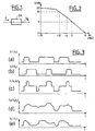
- the gain G varies according to the optical power PE of the input signal E according to a gain curve such that that shown by way of example in FIG. 2. On this figure, the gain is expressed in decibels and the optical power in dBm.
- the gain is constant and the amplifier operates in linear mode.
- the gain value decreases as the power increases.
- the input saturation power of amplifier as the input power for which the gain has a value equal to half the maximum gain of the amplifier, i.e. for a gain expressed in dB 3dB lower than the maximum gain.
- the maximum gain is 20 dB and the power of saturation is -10dBm. Beyond the power of saturation, the gain in dB practically decreases linear as a function of the input optical power in dBm.
- the information carried by the signals E1 and E2 are entered in the form of amplitude modulations (or optical power) of carrier waves having the lengths wave ⁇ 1 and ⁇ 2. These are binary signals with a NRZ coding format.
- the instantaneous optical power of the multiplex signal E is the sum of the instantaneous powers of the two signals El, E2 and then presents an amplitude modulation represented by the timing diagram (c).
- the OA amplifier outputs the signal amplified Sa. Taking into account the gain saturation exposed previously, high power levels are less amplified as low levels and you get modulation distorted as represented by the timing diagram (d). For then extract the channel E1 for example, we perform a filtering calibrated on the wavelength ⁇ 1. We then obtain a filtered signal Sf which has a very distorted modulation, as shown in the timing diagram (e).
- the deformations can be very important and lead to many reading errors in the receiver, even if it's digital signals.
- the device includes the semiconductor optical amplifier OA and Ca coupling means allowing him inject the combination S of the optical signal to be amplified E and an optical compensation wave E *.
- the signal to be amplified E is generally obtained by an input interface Ce receiving an input signal E0 which can be a single wavelength optical signal or, like previously, a WDM signal composed of several signals carried signal wavelength (s) ⁇ i.
- the signal input E0 can also be an electrical signal and in this case, the interface Ce will have a converter function electrooptical.
- the compensation wave E * is produced by modulation means 1 sensitive to the modulation of the input signal E0 and therefore to that of the signal to be amplified E. They are designed to modulate at least one auxiliary optical carrier wave CW, having a so-called compensation wavelength ⁇ c, so that the combination S of the signal E and of the wave E * has an amplitude modulation suppressed or at least attenuated.
- the amplifier OA outputs the amplified combination signal Sa.
- the signal E and the compensation wave E * are codirectional, that is to say injected into the amplifier by the same face.
- a rejector filter F calibrated on the compensation wavelength ⁇ c. It is of course necessary that the compensation wavelength ⁇ c is distinct from the signal wavelength (s) ⁇ i so that the filter can extract the compensation wave E * and transmit the amplified useful signal Sf.
- the signal E and the compensation wave E * are contradictory, that is to say injected into the amplifier by opposite faces.
- the coupling means Ca comprise on the one hand an isolator IS arranged between the input interface Ce and a first face of the amplifier OA, and on the other hand a circulator Ci placed between the modulation means 1 and a second face of the OA amplifier.
- the presence downstream of the rejector filter F is no longer necessary.
- such a filter could replace the IS insulator.
- the wavelength compensation ⁇ c could be close to one of signal wavelengths ⁇ i. However, it should avoid choosing identical wavelengths as this would generate interference noise between the compensation and signal.
- the signal to amplifier E consists of the two channels E1 and E2.
- the signals E1, E2 and E are represented respectively on the chronograms (a), (b) and (c).
- the compensation wave E * is represented by the timing diagram (d).
- the combination signal S whose instantaneous power is the sum of the instantaneous powers of E and E * appears on the timing diagram (e).
- the amplified combination signal Sa appears on the timing diagram (f).
- the compensation wave E * is modulated in reverse with respect to the modulation of the signal E. If the modulation amplitudes of E and E * are at all times strictly equal in absolute value, the combination signal S no longer has any modulation optical power. This ideal case is shown in dotted lines on the timing diagrams (d) and (e).
- the OA amplifier being insensitive to high modulations frequency, it acts as a low-pass filter. If its frequency cutoff is less than that of the modulation means 1, any residual modulation of S will be attenuated by amplification. It will therefore be beneficial to choose a slow OA amplifier, i.e. with a low factor of containment and / or short length.
- FIG. 6 represents a first embodiment of the device according to the invention in the case where it is desired amplify an input signal E0 available only under optical form.
- the input interface Ce consists of an input coupler whose input receives this signal E0.
- a first output of the Ce coupler is coupled to the amplifier OA (not shown) via a delay line 2 and the Ca coupler.
- a second output of the Ce coupler is coupled to the modulation means 1.
- the optical signal to be amplified E here corresponds to a part of the optical input signal E0, delayed by the delay line 2.
- the modulation means 1 receive from the coupler Ce another part e of the optical input signal E0 and supply the amplifier OA, via a Ca coupler, the optical compensation wave E * .
- the modulation means 1 include an electrooptical modulator 3 with structure Mach-Zehnder type interferometry.
- PD photodetector receives part e of the optical input signal E0.
- the signal electric it provides is applied to an electrode of control of modulator 3 via a electronic amplifier 4 and a T-coupler. last allows to superimpose the alternative component of the voltage from photodetector PD at a voltage of Vp polarization chosen.
- a laser source LD delivering the continuous carrier wave CW of wavelength ⁇ c is coupled to the Mach-Zehnder 3 modulator which supplies the optical compensation wave E * as an output.
- the electronic amplifier 4 and the modulator 3 are chosen so that the carrier wave CW is modulated in reverse with respect to the modulation of the signal E0.
- the delay line 2 is used to synchronize the signal to be amplified E with the compensation wave E * .
- the modulation means 1 have a response "anti-linear" with respect to the optical signal sampled and that the power of the wave compensation E * is adjusted accordingly. This latter condition can be satisfied by adjusting the power of the continuous wave CW, by acting on the current I injected into the laser LD.
- the interferometric structure modulator can be replaced by an electro-absorption modulator, such as illustrated in figure 9.
- This variant has the advantage of a linear response over an amplitude range of more extensive modulation.
- the LD laser source and modulator 3 whatever its type, can of course be made so integrated.
- FIG. 8 represents a first all-optical embodiment of the modulation means 1. They in fact consist of a wavelength converter comprising a second semiconductor optical amplifier 5 which receives the auxiliary optical carrier wave CW and , via a circulator 6, the part e of the optical input signal E0.
- the amplifier 5 operates in saturation mode and its gain is modulated as a function of the modulation of the power of e.
- the auxiliary wave CW is amplified with this modulated gain and an e * wave is obtained at the output, the power of which is modulated in inverse relation to the power of e.
- the wave e * is received by the circulator 6 which then supplies the compensation wave E * .
- Amplifier 5 will be chosen to have a cutoff frequency high enough to respond to rapid fluctuations in amplitude of the optical input signal E0 which are insufficiently filtered by the amplifier OA.
- the modulation means 1 have an antilinear response and that the power of the compensation wave E * is properly adjusted.
- account must be taken here of the characteristics of the amplifier 5, that is to say of its gain curve. This curve is similar to that shown in Figure 2.
- the operating point of the amplifier 5 is then practically determined by the average power of e. If the average power (expressed in dBm) of E0 undergoes an increase ⁇ P (E), this results in the same increase in those of E and e. But according to the gain curve, for operation in saturation regime, an increase ⁇ P (E) (in dBm) of the average power of e results in a gain decrease (in decibels) of substantially the same value. The average power (in dBm) of e * and therefore that of E * consequently undergoes a reduction of this same value.
- Such means are shown schematically on the Figure 8. They have a cascade photodetector 8, a low-pass electronic filter 9, an electronic circuit of control 10 and an adjustable current source 11.
- the photodetector 8 is arranged to receive part of the input signal E0.
- the current source 11 delivers to the laser LD a variable current I as a function of a control signal supplied by circuit 10.
- the low-pass filter 9 is used to extract the average power from E.
- the control circuit 10 is provided to produce a control signal which is a function of this measurement and adapted to the characteristics of the amplifier 5 so as to permanently equalize the average power of E and E * .
- the modulation means 1 can consist of a wavelength converter with interferometric structure, for example of the Mach-Zehnder type.
- the interferometric structure is provided with two branches, two ends of which receive part of the CW auxiliary wave.
- the signal e is injected into one of the branches which comprises a material whose index varies as a function of the optical power received.
- the other ends of the branches are coupled to provide the compensation wave E * .
- FIG. 12 Another embodiment shown in Figure 12 concerns the case where the optical signal to be amplified E is produced from an electrical input signal E0 available at the OA amplifier. This situation occurs in transmitting terminals with a emission amplifier usually called "booster".
- the signal to be amplified E is supplied by an electrooptical modulator 11 receiving a wave signal carrier ⁇ i and controlled by the electrical signal E0.
- the modulation means 1 then consist of another electrooptical modulator 12 receiving the auxiliary wave CW and controlled by a complementary electrical signal E0 * from the electrical input signal E0.
Landscapes
- Physics & Mathematics (AREA)
- Electromagnetism (AREA)
- Engineering & Computer Science (AREA)
- Computer Networks & Wireless Communication (AREA)
- Signal Processing (AREA)
- Condensed Matter Physics & Semiconductors (AREA)
- General Physics & Mathematics (AREA)
- Optics & Photonics (AREA)
- Optical Communication System (AREA)
- Semiconductor Lasers (AREA)
- Body Structure For Vehicles (AREA)
Abstract
Description
- des moyens de compensation pour produire une onde optique de compensation,
- des moyens de couplage pour injecter dans ledit
amplificateur ledit signal optique à amplifier et ladite
onde optique de compensation,
et en ce que lesdits moyens de compensation comprennent des moyens de modulation directement commandés en fonction de la modulation du signal à amplifier, pour produire ladite onde optique de compensation par modulation d'amplitude d'au moins une onde porteuse optique auxiliaire, de sorte que la combinaison dudit signal optique à amplifier et de ladite onde optique de compensation présente une modulation d'amplitude supprimée ou au moins atténuée.
- La figure 1 représente un amplificateur optique semi-conducteur utilisé dans la présente invention.
- La figure 2 représente une courbe de gain de l'amplificateur de la figure 1.
- La figure 3 représente des chronogrammes pour expliquer le fonctionnement de l'amplificateur de la figure 1.
- La figure 4 représente schématiquement un dispositif selon l'invention.
- La figure 5 représente des chronogrammes pour expliquer le fonctionnement du dispositif de la figure 4.
- La figure 6 représente un premier mode de réalisation du dispositif selon l'invention.
- La figure 7 est une courbe représentant les variations de la transmission d'un modulateur électrooptique à structure interférométrique.
- La figure 8 représente un second mode de réalisation du dispositif selon l'invention.
- Les figures 9 à 11 représentent des variantes de réalisation des dispositifs selon respectivement les figures 6, 8 et 4.
- La figure 12 représente un troisième mode de réalisation du dispositif selon l'invention.
Claims (12)
- Dispositif pour amplifier au moyen d'un amplificateur optique semi-conducteur (OA) un signal optique modulé en amplitude, appelé signal à amplifier (E), et porté par au moins une longueur d'onde de signal (λi), caractérisé en ce qu'il comporte :des moyens de compensation pour produire une onde optique de compensation (E*),des moyens de couplage (Ca) pour injecter dans ledit amplificateur (OA) ledit signal optique à amplifier (E) et ladite onde optique de compensation (E*),
et en ce que lesdits moyens de compensation comprennent des moyens de modulation (1) commandés directement en fonction de la modulation du signal à amplifier (E), pour produire ladite onde optique de compensation (E*) par modulation d'amplitude d'au moins une onde porteuse optique auxiliaire (CW), de sorte que la combinaison (S) dudit signal optique à amplifier (E) et de ladite onde optique de compensation (E*) présente une modulation d'amplitude supprimée ou au moins atténuée. - Dispositif selon la revendication 1, caractérisé en ce que ladite onde porteuse optique auxiliaire (CW) a une longueur d'onde de compensation (λc) distincte de ladite ou desdites longueur(s) d'onde de signal (λi).
- Dispositif selon l'une des revendications 1 ou 2, caractérisé en ce que lesdits moyens de compensation comportent un dispositif à retard (2) fournissant ledit signal à amplifier (E) à partir d'un signal optique d'entrée (E0) et en ce que lesdits moyens de modulation (1) sont aptes à moduler l'amplitude de ladite onde porteuse optique auxiliaire (CW) en inverse par rapport à la modulation dudit signal d'entrée (E0).
- Dispositif selon la revendication 3, caractérisé en ce que lesdits moyens de modulation (1) comportent un photodétecteur (PD) recevant une partie (e) dudit signal optique d'entrée (E0) et commandant un modulateur électrooptique (3), ladite onde optique de compensation (E*) résultant de la modulation de ladite onde auxiliaire (CW) au moyen dudit modulateur électrooptique (3).
- Dispositif selon la revendication 3, caractérisé en ce que ledit modulateur électrooptique (3) est un modulateur à structure interférométrique.
- Dispositif selon la revendication 3, caractérisé en ce que ledit modulateur électrooptique (3) est un modulateur à électroabsorption.
- Dispositif selon l'une des revendications 5 ou 6, caractérisé en ce que ledit modulateur électrooptique (3) et ladite source laser (LD) sont constitués d'un laser à modulateur intégré.
- Dispositif selon la revendication 3, caractérisé en ce que lesdits moyens de modulation (1) comportent un second amplificateur optique semi-conducteur (5) recevant ladite onde porteuse optique auxiliaire (CW) et une partie (e) dudit signal optique d'entrée (E0), ladite onde optique de compensation (E*) résultant de l'amplification de ladite onde auxiliaire (CW) au moyen dudit second amplificateur (5), dont le gain est modulé par ladite partie (e) du signal optique d'entrée (E0).
- Dispositif selon la revendication 3, caractérisé en ce que lesdits moyens de modulation (1) comportent une structure interférométrique munie de deux branches ayant chacune des première et seconde extrémités, lesdites premières extrémités recevant respectivement une partie de ladite onde auxiliaire (CW), une desdites branches comprenant un matériau dont l'indice varie en fonction de la puissance optique reçue et recevant une partie (e) dudit signal optique d'entrée (E0), lesdites secondes extrémités étant couplées pour fournir ladite onde optique de compensation (E*).
- Dispositif selon l'une des revendications 8 ou 9, caractérisé en ce qu'il comporte des moyens (7, 8, 9, 10, 11) d'ajustement automatique de la puissance moyenne de ladite onde optique de compensation (E*) en fonction de la puissance moyenne dudit signal optique d'entrée (E0).
- Dispositif selon l'une des revendications 1 ou 2, caractérisé en ce que ledit signal optique à amplifier (E) étant produit à partir d'un signal électrique d'entrée (E0), lesdits moyens de modulation (1) sont constitués d'un modulateur électrooptique (12) recevant ladite onde auxiliaire (CW) et commandé par un signal électrique complémentaire (E0*) dudit signal électrique d'entrée (E0).
- Dispositif selon l'une des revendications 1 à 11, caractérisé en ce que ledit amplificateur optique semi-conducteur (OA) possède une fréquence de coupure inférieure à celle desdits moyens de modulation (1).
Applications Claiming Priority (2)
| Application Number | Priority Date | Filing Date | Title |
|---|---|---|---|
| FR0003373 | 2000-03-16 | ||
| FR0003373A FR2806485B1 (fr) | 2000-03-16 | 2000-03-16 | Dispositif d'amplification optique |
Publications (2)
| Publication Number | Publication Date |
|---|---|
| EP1134859A1 true EP1134859A1 (fr) | 2001-09-19 |
| EP1134859B1 EP1134859B1 (fr) | 2007-11-28 |
Family
ID=8848160
Family Applications (1)
| Application Number | Title | Priority Date | Filing Date |
|---|---|---|---|
| EP01400465A Expired - Lifetime EP1134859B1 (fr) | 2000-03-16 | 2001-02-22 | Dispositif d'amplification optique |
Country Status (7)
| Country | Link |
|---|---|
| US (1) | US6473225B1 (fr) |
| EP (1) | EP1134859B1 (fr) |
| JP (1) | JP2001298416A (fr) |
| AT (1) | ATE379862T1 (fr) |
| CA (1) | CA2338873A1 (fr) |
| DE (1) | DE60131587T2 (fr) |
| FR (1) | FR2806485B1 (fr) |
Cited By (1)
| Publication number | Priority date | Publication date | Assignee | Title |
|---|---|---|---|---|
| US6473225B1 (en) * | 2000-03-16 | 2002-10-29 | Alcatel | Light amplifier device |
Families Citing this family (4)
| Publication number | Priority date | Publication date | Assignee | Title |
|---|---|---|---|---|
| WO2004074805A1 (fr) * | 2003-02-18 | 2004-09-02 | Fujitsu Limited | Source de lumiere |
| FR2859795A1 (fr) * | 2003-09-12 | 2005-03-18 | Framatome Connectors Int | Convertisseur electro-optique et dispositif de connexion de type bidirectionnel comportant un tel convertisseur |
| JP5161329B2 (ja) * | 2011-03-09 | 2013-03-13 | 日本電信電話株式会社 | 光送信器および光直交振幅変調方法 |
| CN113810119A (zh) * | 2021-11-05 | 2021-12-17 | 青岛光盈光电技术有限责任公司 | 一种5g前传mwdm系统的光通信系统 |
Citations (2)
| Publication number | Priority date | Publication date | Assignee | Title |
|---|---|---|---|---|
| JPH0317633A (ja) * | 1989-06-15 | 1991-01-25 | Hitachi Ltd | 光インバータ |
| EP0881790A1 (fr) * | 1997-05-29 | 1998-12-02 | Alcatel | Système de transmission optique à compensation dynamique de la puissance transmise |
Family Cites Families (4)
| Publication number | Priority date | Publication date | Assignee | Title |
|---|---|---|---|---|
| US5264960A (en) * | 1992-05-08 | 1993-11-23 | At&T Bell Laboratories | Optical wavelength shifter |
| KR19990055420A (ko) * | 1997-12-27 | 1999-07-15 | 정선종 | 반도체 광 증폭기와 편광 간섭계를 이용한 완전 광 파장 변환기 |
| JP3877942B2 (ja) * | 1999-07-20 | 2007-02-07 | ルーセント テクノロジーズ インコーポレーテッド | 光通信システム動作方法及び光通信システム |
| FR2806485B1 (fr) * | 2000-03-16 | 2003-07-04 | Cit Alcatel | Dispositif d'amplification optique |
-
2000
- 2000-03-16 FR FR0003373A patent/FR2806485B1/fr not_active Expired - Fee Related
-
2001
- 2001-02-22 AT AT01400465T patent/ATE379862T1/de not_active IP Right Cessation
- 2001-02-22 EP EP01400465A patent/EP1134859B1/fr not_active Expired - Lifetime
- 2001-02-22 DE DE60131587T patent/DE60131587T2/de not_active Expired - Lifetime
- 2001-02-26 US US09/791,606 patent/US6473225B1/en not_active Expired - Fee Related
- 2001-02-27 CA CA002338873A patent/CA2338873A1/fr not_active Abandoned
- 2001-03-15 JP JP2001073306A patent/JP2001298416A/ja not_active Withdrawn
Patent Citations (2)
| Publication number | Priority date | Publication date | Assignee | Title |
|---|---|---|---|---|
| JPH0317633A (ja) * | 1989-06-15 | 1991-01-25 | Hitachi Ltd | 光インバータ |
| EP0881790A1 (fr) * | 1997-05-29 | 1998-12-02 | Alcatel | Système de transmission optique à compensation dynamique de la puissance transmise |
Non-Patent Citations (3)
| Title |
|---|
| MA B ET AL: "REALIZATION OF ALL-OPTICAL WAVELEGTH CONVERTER BASED ON DIRECTIONALLY COUPLED SEMICONDUCTOR OPTICAL AMPLIFIERS", IEEE PHOTONICS TECHNOLOGY LETTERS,IEEE INC. NEW YORK,US, vol. 11, no. 2, February 1999 (1999-02-01), pages 188 - 190, XP000803424, ISSN: 1041-1135 * |
| MANABU YOSHINO ET AL: "IMPROVEMENT OF SATURATION OUTPUT POWER IN A SEMICONDUCTOR LASER AMPLIFIER THROUGH PUMPING LIGHT IMJECTION", IEEE PHOTONICS TECHNOLOGY LETTERS,IEEE INC. NEW YORK,US, vol. 8, no. 1, 1996, pages 58 - 59, XP000547533, ISSN: 1041-1135 * |
| PATENT ABSTRACTS OF JAPAN vol. 015, no. 140 (P - 1188) 9 April 1991 (1991-04-09) * |
Cited By (1)
| Publication number | Priority date | Publication date | Assignee | Title |
|---|---|---|---|---|
| US6473225B1 (en) * | 2000-03-16 | 2002-10-29 | Alcatel | Light amplifier device |
Also Published As
| Publication number | Publication date |
|---|---|
| EP1134859B1 (fr) | 2007-11-28 |
| CA2338873A1 (fr) | 2001-09-16 |
| DE60131587T2 (de) | 2008-11-27 |
| ATE379862T1 (de) | 2007-12-15 |
| US6473225B1 (en) | 2002-10-29 |
| FR2806485B1 (fr) | 2003-07-04 |
| DE60131587D1 (de) | 2008-01-10 |
| JP2001298416A (ja) | 2001-10-26 |
| FR2806485A1 (fr) | 2001-09-21 |
Similar Documents
| Publication | Publication Date | Title |
|---|---|---|
| EP0813097B1 (fr) | Dispositif de mise en forme de signaux optiques binaires et son utilisation pour modifier lesdits signaux | |
| FR2774483A1 (fr) | Systeme d'egalisation de gain | |
| FR2521369A1 (fr) | Circuit amplificateur comportant une annulation de la tension de decalage | |
| EP1111820A1 (fr) | Dispositif d'application d'un retard en ligne | |
| CA1311820C (fr) | Source laser a semi-conducteur modulee a frequence elevee | |
| FR2756440A1 (fr) | Dispositif d'emission de donnees optiques | |
| FR2759790A1 (fr) | Convertisseur de longueur d'onde de signaux optiques binaires | |
| EP0881790B1 (fr) | Système de transmission optique à compensation dynamique de la puissance transmise | |
| EP0762576A1 (fr) | Composant opto-électronique intégré | |
| EP0716486A1 (fr) | Dispositif convertisseur de longueur d'onde | |
| EP1134859B1 (fr) | Dispositif d'amplification optique | |
| FR2734677A1 (fr) | Procede d'inscription de donnees binaires sur une onde porteuse, notamment optique, et systeme de transmission utilisant ce procede | |
| EP0999622A1 (fr) | Amplificateur optique à semi-conducteur à gain stabilisé réglable et système optique utilisant un tel amplificateur | |
| FR2787593A1 (fr) | Modulateur de type mach-zehnder presentant un taux d'extinction tres eleve | |
| CA2266058A1 (fr) | Dispositif de mise en forme de signaux optiques binaires | |
| EP0467764B1 (fr) | Système de commutation optique de signaux multiplexés en fréquence | |
| FR2758669A1 (fr) | Procede de modulation et modulateur optique a semi conducteur | |
| EP0901206B1 (fr) | Dispositif préamplificateur optique | |
| EP1306942A1 (fr) | Générateur de brèves impulsions optiques | |
| EP0746070B1 (fr) | Procédé et dispositif pour combiner des signaux optiques | |
| FR2717330A1 (fr) | Modulateur semiconducteur électro-optique et liaison optique incluant ce modulateur. | |
| EP1508984B1 (fr) | Method de formation d'un signal optique code suivant un format retour a zero ou non retour a zero | |
| FR2712096A1 (fr) | Amplificateur optique, émetteur optique, récepteur optique, leur procédé de commande et procédé pour transmettre un signal de contrôle. | |
| EP1363366B1 (fr) | Procédé de stabilisation pour source laser à réflecteur distribué | |
| FR3138219A1 (fr) | puce photonique pourvue d’un modulateur Mach-Zehnder |
Legal Events
| Date | Code | Title | Description |
|---|---|---|---|
| PUAI | Public reference made under article 153(3) epc to a published international application that has entered the european phase |
Free format text: ORIGINAL CODE: 0009012 |
|
| AK | Designated contracting states |
Kind code of ref document: A1 Designated state(s): AT BE CH CY DE DK ES FI FR GB GR IE IT LI LU MC NL PT SE TR |
|
| AX | Request for extension of the european patent |
Free format text: AL;LT;LV;MK;RO;SI |
|
| 17P | Request for examination filed |
Effective date: 20020319 |
|
| AKX | Designation fees paid |
Free format text: AT BE CH CY DE DK ES FI FR GB GR IE IT LI LU MC NL PT SE TR |
|
| RAP1 | Party data changed (applicant data changed or rights of an application transferred) |
Owner name: AVANEX CORPORATION |
|
| GRAP | Despatch of communication of intention to grant a patent |
Free format text: ORIGINAL CODE: EPIDOSNIGR1 |
|
| RIN1 | Information on inventor provided before grant (corrected) |
Inventor name: DORGEUILLE, FRANCOIS Inventor name: LE SAUZE, NICOLAS Inventor name: PONS, ALAIN Inventor name: ZAMI, THIERRY Inventor name: EMERY, JEAN-YVES Inventor name: CHIARONI, DOMINIQUE |
|
| GRAS | Grant fee paid |
Free format text: ORIGINAL CODE: EPIDOSNIGR3 |
|
| GRAA | (expected) grant |
Free format text: ORIGINAL CODE: 0009210 |
|
| AK | Designated contracting states |
Kind code of ref document: B1 Designated state(s): AT BE CH CY DE DK ES FI FR GB GR IE IT LI LU MC NL PT SE TR |
|
| REG | Reference to a national code |
Ref country code: GB Ref legal event code: FG4D Free format text: NOT ENGLISH |
|
| REG | Reference to a national code |
Ref country code: IE Ref legal event code: FG4D Free format text: LANGUAGE OF EP DOCUMENT: FRENCH |
|
| REG | Reference to a national code |
Ref country code: CH Ref legal event code: EP |
|
| GBT | Gb: translation of ep patent filed (gb section 77(6)(a)/1977) |
Effective date: 20071219 |
|
| REF | Corresponds to: |
Ref document number: 60131587 Country of ref document: DE Date of ref document: 20080110 Kind code of ref document: P |
|
| PG25 | Lapsed in a contracting state [announced via postgrant information from national office to epo] |
Ref country code: ES Free format text: LAPSE BECAUSE OF FAILURE TO SUBMIT A TRANSLATION OF THE DESCRIPTION OR TO PAY THE FEE WITHIN THE PRESCRIBED TIME-LIMIT Effective date: 20080311 Ref country code: SE Free format text: LAPSE BECAUSE OF FAILURE TO SUBMIT A TRANSLATION OF THE DESCRIPTION OR TO PAY THE FEE WITHIN THE PRESCRIBED TIME-LIMIT Effective date: 20080228 Ref country code: NL Free format text: LAPSE BECAUSE OF FAILURE TO SUBMIT A TRANSLATION OF THE DESCRIPTION OR TO PAY THE FEE WITHIN THE PRESCRIBED TIME-LIMIT Effective date: 20071128 |
|
| NLV1 | Nl: lapsed or annulled due to failure to fulfill the requirements of art. 29p and 29m of the patents act | ||
| PG25 | Lapsed in a contracting state [announced via postgrant information from national office to epo] |
Ref country code: FI Free format text: LAPSE BECAUSE OF FAILURE TO SUBMIT A TRANSLATION OF THE DESCRIPTION OR TO PAY THE FEE WITHIN THE PRESCRIBED TIME-LIMIT Effective date: 20071128 |
|
| PG25 | Lapsed in a contracting state [announced via postgrant information from national office to epo] |
Ref country code: AT Free format text: LAPSE BECAUSE OF FAILURE TO SUBMIT A TRANSLATION OF THE DESCRIPTION OR TO PAY THE FEE WITHIN THE PRESCRIBED TIME-LIMIT Effective date: 20071128 |
|
| PG25 | Lapsed in a contracting state [announced via postgrant information from national office to epo] |
Ref country code: DK Free format text: LAPSE BECAUSE OF FAILURE TO SUBMIT A TRANSLATION OF THE DESCRIPTION OR TO PAY THE FEE WITHIN THE PRESCRIBED TIME-LIMIT Effective date: 20071128 |
|
| BERE | Be: lapsed |
Owner name: VANEX CORP. Effective date: 20080228 |
|
| PG25 | Lapsed in a contracting state [announced via postgrant information from national office to epo] |
Ref country code: PT Free format text: LAPSE BECAUSE OF FAILURE TO SUBMIT A TRANSLATION OF THE DESCRIPTION OR TO PAY THE FEE WITHIN THE PRESCRIBED TIME-LIMIT Effective date: 20080428 |
|
| REG | Reference to a national code |
Ref country code: CH Ref legal event code: PL |
|
| REG | Reference to a national code |
Ref country code: IE Ref legal event code: FD4D |
|
| PLBE | No opposition filed within time limit |
Free format text: ORIGINAL CODE: 0009261 |
|
| STAA | Information on the status of an ep patent application or granted ep patent |
Free format text: STATUS: NO OPPOSITION FILED WITHIN TIME LIMIT |
|
| PG25 | Lapsed in a contracting state [announced via postgrant information from national office to epo] |
Ref country code: LI Free format text: LAPSE BECAUSE OF NON-PAYMENT OF DUE FEES Effective date: 20080229 Ref country code: IE Free format text: LAPSE BECAUSE OF FAILURE TO SUBMIT A TRANSLATION OF THE DESCRIPTION OR TO PAY THE FEE WITHIN THE PRESCRIBED TIME-LIMIT Effective date: 20071128 Ref country code: CH Free format text: LAPSE BECAUSE OF NON-PAYMENT OF DUE FEES Effective date: 20080229 Ref country code: MC Free format text: LAPSE BECAUSE OF NON-PAYMENT OF DUE FEES Effective date: 20080228 |
|
| 26N | No opposition filed |
Effective date: 20080829 |
|
| PG25 | Lapsed in a contracting state [announced via postgrant information from national office to epo] |
Ref country code: GR Free format text: LAPSE BECAUSE OF FAILURE TO SUBMIT A TRANSLATION OF THE DESCRIPTION OR TO PAY THE FEE WITHIN THE PRESCRIBED TIME-LIMIT Effective date: 20080229 |
|
| PG25 | Lapsed in a contracting state [announced via postgrant information from national office to epo] |
Ref country code: BE Free format text: LAPSE BECAUSE OF NON-PAYMENT OF DUE FEES Effective date: 20080228 |
|
| PG25 | Lapsed in a contracting state [announced via postgrant information from national office to epo] |
Ref country code: CY Free format text: LAPSE BECAUSE OF FAILURE TO SUBMIT A TRANSLATION OF THE DESCRIPTION OR TO PAY THE FEE WITHIN THE PRESCRIBED TIME-LIMIT Effective date: 20071128 |
|
| PG25 | Lapsed in a contracting state [announced via postgrant information from national office to epo] |
Ref country code: LU Free format text: LAPSE BECAUSE OF NON-PAYMENT OF DUE FEES Effective date: 20080222 |
|
| PG25 | Lapsed in a contracting state [announced via postgrant information from national office to epo] |
Ref country code: TR Free format text: LAPSE BECAUSE OF FAILURE TO SUBMIT A TRANSLATION OF THE DESCRIPTION OR TO PAY THE FEE WITHIN THE PRESCRIBED TIME-LIMIT Effective date: 20071128 |
|
| PGFP | Annual fee paid to national office [announced via postgrant information from national office to epo] |
Ref country code: FR Payment date: 20120221 Year of fee payment: 12 |
|
| PGFP | Annual fee paid to national office [announced via postgrant information from national office to epo] |
Ref country code: DE Payment date: 20120215 Year of fee payment: 12 |
|
| PGFP | Annual fee paid to national office [announced via postgrant information from national office to epo] |
Ref country code: IT Payment date: 20120218 Year of fee payment: 12 Ref country code: GB Payment date: 20120222 Year of fee payment: 12 |
|
| GBPC | Gb: european patent ceased through non-payment of renewal fee |
Effective date: 20130222 |
|
| REG | Reference to a national code |
Ref country code: FR Ref legal event code: ST Effective date: 20131031 |
|
| REG | Reference to a national code |
Ref country code: DE Ref legal event code: R119 Ref document number: 60131587 Country of ref document: DE Effective date: 20130903 |
|
| PG25 | Lapsed in a contracting state [announced via postgrant information from national office to epo] |
Ref country code: IT Free format text: LAPSE BECAUSE OF NON-PAYMENT OF DUE FEES Effective date: 20130222 |
|
| PG25 | Lapsed in a contracting state [announced via postgrant information from national office to epo] |
Ref country code: FR Free format text: LAPSE BECAUSE OF NON-PAYMENT OF DUE FEES Effective date: 20130228 Ref country code: DE Free format text: LAPSE BECAUSE OF NON-PAYMENT OF DUE FEES Effective date: 20130903 Ref country code: GB Free format text: LAPSE BECAUSE OF NON-PAYMENT OF DUE FEES Effective date: 20130222 |