EP1134802A2 - Method of forming conducting diffusion barriers - Google Patents
Method of forming conducting diffusion barriers Download PDFInfo
- Publication number
- EP1134802A2 EP1134802A2 EP01302248A EP01302248A EP1134802A2 EP 1134802 A2 EP1134802 A2 EP 1134802A2 EP 01302248 A EP01302248 A EP 01302248A EP 01302248 A EP01302248 A EP 01302248A EP 1134802 A2 EP1134802 A2 EP 1134802A2
- Authority
- EP
- European Patent Office
- Prior art keywords
- film
- implanted
- deposited
- plasma
- initial
- Prior art date
- Legal status (The legal status is an assumption and is not a legal conclusion. Google has not performed a legal analysis and makes no representation as to the accuracy of the status listed.)
- Withdrawn
Links
Images


Classifications
-
- H—ELECTRICITY
- H10—SEMICONDUCTOR DEVICES; ELECTRIC SOLID-STATE DEVICES NOT OTHERWISE PROVIDED FOR
- H10P—GENERIC PROCESSES OR APPARATUS FOR THE MANUFACTURE OR TREATMENT OF DEVICES COVERED BY CLASS H10
- H10P14/00—Formation of materials, e.g. in the shape of layers or pillars
- H10P14/20—Formation of materials, e.g. in the shape of layers or pillars of semiconductor materials
-
- H—ELECTRICITY
- H10—SEMICONDUCTOR DEVICES; ELECTRIC SOLID-STATE DEVICES NOT OTHERWISE PROVIDED FOR
- H10W—GENERIC PACKAGES, INTERCONNECTIONS, CONNECTORS OR OTHER CONSTRUCTIONAL DETAILS OF DEVICES COVERED BY CLASS H10
- H10W20/00—Interconnections in chips, wafers or substrates
- H10W20/01—Manufacture or treatment
- H10W20/031—Manufacture or treatment of conductive parts of the interconnections
- H10W20/032—Manufacture or treatment of conductive parts of the interconnections of conductive barrier, adhesion or liner layers
- H10W20/047—Manufacture or treatment of conductive parts of the interconnections of conductive barrier, adhesion or liner layers by introducing additional elements therein
- H10W20/051—Manufacture or treatment of conductive parts of the interconnections of conductive barrier, adhesion or liner layers by introducing additional elements therein by ion implantation
-
- H—ELECTRICITY
- H10—SEMICONDUCTOR DEVICES; ELECTRIC SOLID-STATE DEVICES NOT OTHERWISE PROVIDED FOR
- H10W—GENERIC PACKAGES, INTERCONNECTIONS, CONNECTORS OR OTHER CONSTRUCTIONAL DETAILS OF DEVICES COVERED BY CLASS H10
- H10W20/00—Interconnections in chips, wafers or substrates
- H10W20/01—Manufacture or treatment
- H10W20/031—Manufacture or treatment of conductive parts of the interconnections
- H10W20/032—Manufacture or treatment of conductive parts of the interconnections of conductive barrier, adhesion or liner layers
- H10W20/033—Manufacture or treatment of conductive parts of the interconnections of conductive barrier, adhesion or liner layers in openings in dielectrics
-
- H—ELECTRICITY
- H10—SEMICONDUCTOR DEVICES; ELECTRIC SOLID-STATE DEVICES NOT OTHERWISE PROVIDED FOR
- H10W—GENERIC PACKAGES, INTERCONNECTIONS, CONNECTORS OR OTHER CONSTRUCTIONAL DETAILS OF DEVICES COVERED BY CLASS H10
- H10W20/00—Interconnections in chips, wafers or substrates
- H10W20/01—Manufacture or treatment
- H10W20/031—Manufacture or treatment of conductive parts of the interconnections
- H10W20/032—Manufacture or treatment of conductive parts of the interconnections of conductive barrier, adhesion or liner layers
- H10W20/052—Manufacture or treatment of conductive parts of the interconnections of conductive barrier, adhesion or liner layers by treatments not introducing additional elements therein
- H10W20/0526—Manufacture or treatment of conductive parts of the interconnections of conductive barrier, adhesion or liner layers by treatments not introducing additional elements therein by thermal treatment thereof
Definitions
- This invention relates generally to semiconductor technology and more particularly to a method of forming conducting diffusion barriers for semiconductor devices.
- Diffusion barriers are commonly used in integrated circuit (IC) fabrication to prevent interdiffusion of metals.
- IC integrated circuit
- a TiN film is used to prevent diffusion of Al into Si at contact regions and along metal lines.
- Thinner barriers are required without substantially increasing resistivity. Barriers also need to be more resistant to diffusion of various new metals, which are being introduced into production processes.
- One of the metals that is being introduced is copper.
- few diffusion barriers materials effectively block the diffusion of copper, metal nitride and silicon nitride have been shown to act as good barriers against copper diffusion.
- thin films with desired composition and conductivity cannot be easily deposited. This is especially true for ternary or quaternary materials.
- ICs typically have structures at different heights. These structures form steps. Many of the materials being investigated for use as diffusion barriers, do not have good step coverage when deposited using conventional means. For instance, conventional sputtering methods suffer from problems of poor step coverage and composition control, especially for ternary or quaternary materials.
- Step coverage refers to the ability of a deposited material to follow the underlying stap to provide desirable coverage. Step coverage is defined in terms of the ratio of the thickness of the thinnest region, which is typically at the bottom corners, versus the thickness of the material deposited over a flat upper region, expressed as a percentage. Step coverage is considered good if it is equal to or greater than 70%.
- a method of forming a diffusion barrier comprises the steps of:
- the semiconductor substrata is annealed to reduce or eliminate implant damage and achieve the appropriate composition and crystallinity.
- Metal is preferably deposited within a trench to form a metal line.
- the layer of initial material is formed by chemical vapor deposition (CVD), plasma-enhanced chemical vapor deposition (PECVD), or ion metal plasma (IMP) deposition.
- Deposition is preferably a low temperature deposition at less than 450 degrees Celsius.
- the initial material can be selected from a wide variety of materials. The initial material need not have good conductivity or barrier properties. Preferably, the initial material will provide good step coverage, and provide at least some of the material necessary to produce a final desired material having sufficient conductivity and barrier properties for the desired metal line.
- the initial material can comprise a single element, a binary material, or even, ternary or quaternary materials, provided they have adequate step coverage.
- binary, ternary, and quaternary are used through out this specification to refer to materials having two elements, three elements, and four elements, respectively. In common usage, these terms refer to compounds. As used herein, these terms may include compounds, alloys or other categories of materials having the designated number of elements.
- the implanted ions are implanted to modify the initial material.
- the implanted ions should be selected such that they improve the properties of the initial material, or assist in converting the new material into a desired material.
- the implanted ions should aid in producing materials having good conductivity and barrier properties.
- the ion will be implanted using plasma immersion ion implantation (PIII).
- the substrate will be placed within a PIII chamber.
- a gas containing a desired element is introduced into the PIII chamber and energized to form a plasma of ionized gas.
- the ions contained within the ionized gas are implanted into the silicon substrata,
- the substrate will be negatively biased to attract the positive ions.
- PIII is preferred, it is also possible to implant the ions by convention ion implantation methods or using ion metal plasma (IMP) techniques.
- IMP ion metal plasma
- the entire semiconductor substrate is annealed to condition the implanted material.
- a rapid thermal anneal (RTA) process is applied to the wafer to anneal out implant damage and to achieve the appropriate composition and crystallinity.
- a convention heat treatment is applied to the wafer using a furnace.
- Subsequent processing can be performed to complete the formation of the barrier layer, including depositing a metal layer.
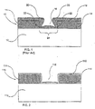
- FIG. 1 is a schematic cross-sectional view showing an integrated circuit (IC) structure with a conventionally deposited barrier layer (prior art).
- FIG. 2 is a schematic cross-sectional view showing an IC structure during processing with an initial material deposited to form a layer.
- FIG. 3 is a schematic cross-sectional view showing ions being implanted into the layer of initial material.
- FIG. 4 is a schematic cross-sectional view showing the layer following implantation and anneal.
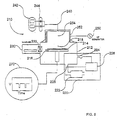
- FIG. 5 is a schematic view showing a plasma ion immersion implantation system.
- FIG. 6 is a flow chart summarizing the steps in the method of the present invention.
- FIG. 1 illustrates the prior art problems related to poor step coverage.
- a partially completed IC device 10 comprises a semiconductor substrate 12 with isolation regions 14 forming a trench 16.
- a diffusion barrier layer 18 has been deposited. Due to poor step coverage, over accumulation regions 20 were formed along with thinner regions 22. As the length 24 of trench 16 diminishes, eventually the over accumulation regions 20 will prevent subsequent metal layers from being properly deposited within the trench 16. In addition, due to the poor step coverage uniform thickness is not maintained along the bottom of the trench 16.
- FIGS. 2-4 illustrate the steps of the method of the present invention.
- a partially completed IC device 110 is provided having a semiconductor substrate 112 with isolation regions 114 forming a trench 116.
- semiconductor substrate 112 is depicted as a single conductive layer, the method of the present invention is well suited to more complicated configurations, including metal layers overlying previously deposited metal layers and interconnecting vias.
- a layer 150, also referred to as a film, of an initial material is deposited using conventional deposition techniques. As shown in FIG. 2, the initial material is deposited with good step coverage, preferably equal to or greater than approximately 70%. The initial material is selected such that it will aid in forming a desired material upon completion of the method of the present invention.
- the initial material need not have good conductivity or good barrier properties in and of itself.
- Layer 150 is preferably formed using chemical vapor deposition (CVD), plasma-enhanced chemical vapor deposition (PECVD) or ion metal plasma (IMP) deposition.
- the initial material is preferably one that is well suited to low temperature CVD or PECVD techniques. Low temperature processing is preferred, because high temperature processes may adversely affect materials and structures that were previously formed.
- the initial material is preferably a binary, such as Si-N, Ti-N, W-N, W-Si, Ti-Si, Ta-Si Ta-N, Si-C, or B-N; or, alternatively, an elemental film such as Si, Ti, W, Ta, Ru, Mo, C, or B. It would also be possible to deposit a combination of multiple elemental materials, multiple binary materials or a combination of both. It is also within the scope of this invention to deposit ternary or other more complicated materials, provided that the material can be deposited with good step coverage.
- the initial material of layer 150 is modified by implanting ions 155 (represented by arrows).
- Ions 155 change one or more of the characteristics of the desired material upon completion of the method of the present invention.
- Ions 155 modify layer 150 to produce a material with good conductivity, good barrier properties, or both. It is not always convenient, or possible, to initially deposit a film with a desired ratio of elements.
- the method of the present invention allows for the deposition of a film followed by implanting to change the ratio of the elements within the film.
- ions 155 are selected from one of the elements forming a previously deposited material.
- tantalum-nitride Ta-N
- tantalum Ta is implanted into the previously deposited film. Increasing the amount of Ta by implanting will reduce resistivity. This technique is also useful in connection with Ti-N films, or other films.
- the initial material of layer 150 is modified by implanting ions 155 that include an element that was not previously deposited.
- W-Si is deposited to form layer 150.
- Nitrogen (N) is then implanted into the film to form the desired W-Si-N.
- a film of W-Si-N is produced by depositing a layer of Si-N and implanting W. It is also within the scope of the present invention to implant more than one element. If a thin film of Si is deposited, both W and N are implanted to form the desired W-Si-N film of desired composition.
- the method of the present invention can be used to produce quaternary or more complex materials.
- Si-N is deposited and implanted with B and Ta to form Ta-B-Si-N.
- the implant is preferably accomplished by depositing one material at a time in order to provide better control of implant dosage, however, it may also be possible to introduce both materials simultaneously.
- layer 150 is annealed to remove implant damage and to achieve the appropriate composition and crystallinity. Conventional heat treatment or rapid thermal annealing process are used to anneal layer 150.
- FIG. 4 shows layer 150 after implant and anneal. Sidewalls 160 did not receive as high of an implant dose as upper areas 170 or bottom 180 of trench 116. Although sidewalls 160 do not receive as high of an implant dose, for many applications the sidewalls are less critical in terms of barrier or conductivity properties. It is also possible to increase the implant dose along sidewalls 160 by changing the placement of the wafer within the plasma chamber to provide a variety of implant angles.
- FIG. 5 shows a schematic illustration of a suitable plasma immersion ion implantation system 210 for carrying out the ion implant step of the present invention.
- Plasma immersion ion implantation system 210 includes a plasma chamber 212 of a size suitable for holding one or more substrates 214, which are supported in the chamber on a chuck 216.
- Substrate 214 is also commonly referred to as a "wafer”.
- the interior 218 of the chamber 212 can be evacuated, and its pressure regulated, by a pressure control system 220.
- Pressure control system 220 includes a pump 222 for exhausting spent gases and contaminants, if any.
- a pressure sensor 224 is connected to a pressure controller 226, which controls a throttle valve 228.
- pressure controller 226 determines that sensor 224 has detected a pressure within interior 218 of the chamber 212 that is outside a predetermined range, pressure controller 226 adjusts valve 228 as necessary to compensate and return the pressure to within the predetermined range.
- individual substrates 214 can be moved in and out of chamber 212 by a suitable handler 230 through a gate valve 232 in a chamber wall, allowing substrates to be moved onto a chuck 216 for processing, and then removed from chamber 212.
- the mechanism by which substrates 214 are moved into the chamber is not critical to the method of the present invention.
- Selected gases used in plasma doping during the ion implantation step are introduced into the chamber 212 through a suitable manifold system 240 from various gas supply reservoirs indicated collectively at 242, controlled by valves indicated at 244. For simplicity only two gas supply reservoirs are shown. It is entirely possible, and not inconsistent with the present invention, to have additional gas supply reservoirs, or only a single gas supply reservoir.
- the manifold system 240 which is shown schematically, may include a gas inlet for blending the gases or a showerhead for distributing the gases within chamber 212 (neither of which are shown).
- Plasma energy is supplied to the chamber 212 by an RF generator 250 that typically supplies high frequency (HF) RF power through coils 252 to energize gases within the chamber forming a plasma within plasma formation region 254.
- HF high frequency
- the process of energizing gases to form a plasma is also referred to as "igniting a plasma”.
- An inductively coupled plasma of between 300 and 3000 watts is used within chamber 212 at a pressure of between approximately 10 and 100 mT.
- the plasma contains implant ions 155 used to modify layer 150 (see FIG. 3).
- the plasma may contain additional ions, including dilutant gas ions.
- nitrogen the plasma comprises nitrogen, or nitrogen mixed with an inert dilutant gas, such as argon (Ar).
- an inert dilutant gas such as argon (Ar).
- tantalum which is not generally a gas at the temperatures and pressures used in the method of the present invention, a gas of TaF 6 would be used along with an inert dilutant gas or hydrogen.
- tungsten (W) a gas of WF 6 would be used along with an inert dilutant gas or hydrogen.
- TiCl 4 a gas of TiCl 4 would be used along with an inert dilutant gas or hydrogen.
- the actual gas selected will depend upon which implant ion is to be implanted. The above examples are for illustration purposes, numerous additional gases containing desired elements can be readily determined, without undue experimentation, by one of ordinary skill in the art. These additional gases are also within the scope of the present invention. Although it is preferable to use a dilutant gas or hydrogen, it is not necessary to the present invention.
- substrate 214 is preferably biased with a negative voltage to attract the positive ions formed within the plasma.
- the negative voltage bias will be pulsed. Pulsing allows the implanted ions to return to an electrically neutral state, which helps to avoid an accumulation of positive charge along the surface of the substrate 214.
- the pulsed negative voltage bias is applied to the substrate 214 by a pulse generator 270, shown schematically connected to the chuck 216.
- the pulses are between approximately 50 volts (V) and 10 kV, but preferably 1 kV.
- the pulse width is between approximately 10 microseconds and 1000 microseconds, but preferably approximately 100 microseconds, at a frequency between approximately 100 Hz and 5 kHz, but preferably 500 Hz.
- the steps in the method of the present invention are illustrated schematically in FIG. 6.
- the first step 510 is to provide a semiconductor substrate.
- the semiconductor substrate will have a trench, or contact, open to the underlying device, or multiple metal layers and interconnects, or vias as necessary to provide connections across a final device after processing.
- Step 520 is the depositing of a thin layer of less than 500 ⁇ of an initial material, such as Si, Ti, W, Ta, Ru, Mo, C, B, Si-N, Ti-N, Ti-Si, W-N, W-Si, Ta-Si, Ta-N, Si-C, or B-N.
- an initial material such as Si, Ti, W, Ta, Ru, Mo, C, B, Si-N, Ti-N, Ti-Si, W-N, W-Si, Ta-Si, Ta-N, Si-C, or B-N.
- the initial material will be between approximately 25 ⁇ and 100 ⁇ , but preferably 50 ⁇ .
- CVD chemical vapor deposition
- TDMAT Tetrakis (DiMethylAmino) Titanium
- Ti-N Tetrakis (DiMethylAmino) Titanium
- TDMAT Tetrakis (DiMethylAmino) Titanium
- the substrate would be exposed to the precursor at a temperature of between 350 and 450 degrees Celsius.
- PECVD plasma-enhanced chemical vapor deposition
- W 2 N tungsten nitride
- W 2 N tungsten nitride
- IMP ion metal plasma
- PVD physical vapor deposition
- IMP sputtering refers to deposition sputtering, where sputtered target material is passed througk an ionization means, such as an inductively coupled RF source, to create a high density, inductively coupled RF plasma between the sputtering target material and the substrate. This ensures that a higher portion of the sputtered emission is in the form of ions at the time it reaches the substrate surface.
- the substrata toward which the sputtered ions are moving is typically biased to attract the incoming ions.
- Step 530 is the implanting of one or more elements to modify the properties of the initial material
- the implanted elements are preferably selected from Si, N, Ti, W, Ta, C, B, P, O, Cl or F. Although, only a single element will preferably be implanted at one time, it is also possibly to implant multiple elements simultaneously or in sequence.
- the step of implanting is accomplished by plasma immersion ion implantation (PIII).
- the substrates are introduced into a plasma chamber, and exposed to a plasma containing ions, as described above with reference to FIG. 5.
- nitrogen is implanted at energies between approximately 0.1 keV and 2 keV, at a dose between 1 ⁇ 10 13 /cm 2 and 1 ⁇ 10 16 /cm 2 , in the preferred embodiment.
- Implantation time varies from 10 seconds to 3 minutes.
- PIII is preferred because of its lower energy, and higher dosage characteristics, the step of implanting is also possible using conventional ion beam implantation methods.
- the ions could be implanted using ion metal plasma (IMP)
- IMP ion metal plasma
- IMP is similar in some ways to PIII, but utilizes a sputter target instead of a gas to introduce the desired implant ions.
- a solid target comprising Ta, Ti, W or other solid material could be used.
- IMP ion metal plasma
- Step 540 is the annealing of the implanted material
- the wafer, including the implanted material is heat treated using a furnace or a rapid thermal anneal process to anneal out implant damage and to achieve the appropriate composition and crystallinity.
- Step 550 is the deposition of a metal film and subsequent processing according to any state of the art methods.
- the metal film is aluminum, copper or any other desired metal.
- the present invention is also well suited to the formation of more complicated trench structures, including multiple conductive layers and vias.
Landscapes
- Internal Circuitry In Semiconductor Integrated Circuit Devices (AREA)
- Electrodes Of Semiconductors (AREA)
- Physical Vapour Deposition (AREA)
- Chemical Vapour Deposition (AREA)
Abstract
Description
Claims (20)
- A method of forming a conducting barrier for integrated circuits comprising the steps of:a) providing a semiconductor substrate;b) depositing a layer of an initial material; andc) implanting ions into the initial material to form a desired material.
- The method of claim 1, wherein the initial material comprises an elemental material.
- The method of claim 1, wherein the initial material comprises a binary material.
- The method of claim 1, wherein the desired material is a binary material.
- The method of claim 1, wherein the desired material is a ternary material.
- The method of claim 1, wherein the desired material is a quaternary material.
- A method of forming a thin conducting film comprising the steps of:a) providing a substrate;b) depositing a film over the substrate;C) implanting an element into the film to form an implanted film;d) annealing the implanted film; ande) depositing a metal film over the implanted film.
- The method of claim 7, wherein the step of depositing the film over the substrate further comprises depositing the film over structures at different heights on the substrate.
- The method of claim 7, wherein the film is less than approximately 1000 angstroms thick.
- The method of claim 7, wherein the film is deposited using chemical vapor deposition (CVD).
- The method of claim 7, wherein the film is deposited using plasma enhanced chemical vapor deposition.
- The method of claim 7, wherein the film is deposited using ion metal plasma deposition.
- The method of claim 10, wherein the film can be deposited using low-temperature CVD.
- The method of claim 7, wherein the film comprises a material selected from the group consisting of Si, Ti, W, Ta, Ru, Mo, C, and B.
- The method of claim 7, wherein the film comprises a material selected from the group consisting of Si-N, Ti-N, Ti-Si, W-N, W-Si, Ta-Si, Ta-N, Si-C, and B-N.
- The method of claim 7, wherein the implanted element comprise a material selected from the group consisting of Si, N, Ti, W, Ta. C, B, P, O, Cl, and F.
- The method of claim 7, wherein the implanted film formed is Ta-N, Ti-N, W-Si-N, Ta-Si-N, Ti-Si-N or Ta-B-Si-N.
- The method of claim 7, further comprising implanting a second element into the film.
- The method of claim 7, wherein the element is implanted using plasma immersion ion implantation.
- The method of claim 7, wherein the element is implanted using ion metal plasma.
Applications Claiming Priority (2)
| Application Number | Priority Date | Filing Date | Title |
|---|---|---|---|
| US527541 | 1983-08-29 | ||
| US09/527,541 US6410383B1 (en) | 2000-03-16 | 2000-03-16 | Method of forming conducting diffusion barriers |
Publications (2)
| Publication Number | Publication Date |
|---|---|
| EP1134802A2 true EP1134802A2 (en) | 2001-09-19 |
| EP1134802A3 EP1134802A3 (en) | 2003-04-02 |
Family
ID=24101873
Family Applications (1)
| Application Number | Title | Priority Date | Filing Date |
|---|---|---|---|
| EP01302248A Withdrawn EP1134802A3 (en) | 2000-03-16 | 2001-03-12 | Method of forming conducting diffusion barriers |
Country Status (5)
| Country | Link |
|---|---|
| US (1) | US6410383B1 (en) |
| EP (1) | EP1134802A3 (en) |
| JP (1) | JP2001308183A (en) |
| KR (1) | KR100407238B1 (en) |
| TW (1) | TW483164B (en) |
Cited By (5)
| Publication number | Priority date | Publication date | Assignee | Title |
|---|---|---|---|---|
| WO2007005873A1 (en) * | 2005-07-01 | 2007-01-11 | Spansion Llc | Preamorphization to minimize void information |
| CN102623389A (en) * | 2011-01-31 | 2012-08-01 | 北京泰龙电子技术有限公司 | A kind of preparation method of metal nitride barrier layer |
| CN102623434A (en) * | 2011-01-31 | 2012-08-01 | 北京泰龙电子技术有限公司 | Diffusion barrier layer and preparation method thereof |
| CN102623435A (en) * | 2011-01-31 | 2012-08-01 | 北京泰龙电子技术有限公司 | Barrier layer and preparation method thereof |
| CN102623311A (en) * | 2011-01-31 | 2012-08-01 | 北京泰龙电子技术有限公司 | A device for preparing metal nitride barrier layer and its use method |
Families Citing this family (23)
| Publication number | Priority date | Publication date | Assignee | Title |
|---|---|---|---|---|
| JP3613113B2 (en) * | 2000-01-21 | 2005-01-26 | 日本電気株式会社 | Semiconductor device and manufacturing method thereof |
| DE10021871A1 (en) * | 2000-05-05 | 2001-11-15 | Infineon Technologies Ag | Method for producing a barrier layer in an electronic component and method for producing an electronic component with a barrier layer |
| US6579788B1 (en) * | 2000-09-18 | 2003-06-17 | Advanced Micro Devices, Inc. | Method of forming conductive interconnections on an integrated circuit device |
| US6835655B1 (en) * | 2001-11-26 | 2004-12-28 | Advanced Micro Devices, Inc. | Method of implanting copper barrier material to improve electrical performance |
| US6703308B1 (en) | 2001-11-26 | 2004-03-09 | Advanced Micro Devices, Inc. | Method of inserting alloy elements to reduce copper diffusion and bulk diffusion |
| US7696092B2 (en) | 2001-11-26 | 2010-04-13 | Globalfoundries Inc. | Method of using ternary copper alloy to obtain a low resistance and large grain size interconnect |
| US6703307B2 (en) | 2001-11-26 | 2004-03-09 | Advanced Micro Devices, Inc. | Method of implantation after copper seed deposition |
| KR100450470B1 (en) * | 2001-12-20 | 2004-10-01 | 주성엔지니어링(주) | Ru thin film forming method using plasma enhanced process |
| US6861349B1 (en) | 2002-05-15 | 2005-03-01 | Advanced Micro Devices, Inc. | Method of forming an adhesion layer with an element reactive with a barrier layer |
| US7169706B2 (en) * | 2003-10-16 | 2007-01-30 | Advanced Micro Devices, Inc. | Method of using an adhesion precursor layer for chemical vapor deposition (CVD) copper deposition |
| US7101787B1 (en) * | 2004-04-09 | 2006-09-05 | National Semiconductor Corporation | System and method for minimizing increases in via resistance by applying a nitrogen plasma after a titanium liner deposition |
| US20060205192A1 (en) * | 2005-03-09 | 2006-09-14 | Varian Semiconductor Equipment Associates, Inc. | Shallow-junction fabrication in semiconductor devices via plasma implantation and deposition |
| US7329599B1 (en) * | 2005-03-16 | 2008-02-12 | Advanced Micro Devices, Inc. | Method for fabricating a semiconductor device |
| US7524743B2 (en) * | 2005-10-13 | 2009-04-28 | Varian Semiconductor Equipment Associates, Inc. | Conformal doping apparatus and method |
| DE102007004884A1 (en) * | 2007-01-31 | 2008-08-14 | Advanced Micro Devices, Inc., Sunnyvale | A method of forming a metal layer over a patterned dielectric by electroless deposition using a selectively provided activation layer |
| JP2010141223A (en) * | 2008-12-15 | 2010-06-24 | Hitachi Kokusai Electric Inc | Method of manufacturing semiconductor device and substrate processing apparatus |
| JP2011162851A (en) * | 2010-02-10 | 2011-08-25 | Fujifilm Corp | Gas barrier film manufacturing method |
| KR101830193B1 (en) * | 2010-07-02 | 2018-02-20 | 가부시키가이샤 한도오따이 에네루기 켄큐쇼 | Semiconductor device and manufacturing method thereof |
| US8461683B2 (en) * | 2011-04-01 | 2013-06-11 | Intel Corporation | Self-forming, self-aligned barriers for back-end interconnects and methods of making same |
| CN103021931B (en) * | 2011-09-23 | 2015-09-23 | 北京泰龙电子技术有限公司 | A kind of preparation method of metal nitride barrier layer |
| KR20130116099A (en) * | 2012-04-13 | 2013-10-23 | 삼성전자주식회사 | Semiconductor device and method for fabricating the same |
| CN104124196B (en) * | 2013-04-23 | 2018-10-23 | 中芯国际集成电路制造(上海)有限公司 | A method of making semiconductor devices |
| US11262495B1 (en) * | 2017-10-04 | 2022-03-01 | Facebook Technologies, Llc | Waveguides with high refractive index gratings manufactured by post-patterning infusion |
Family Cites Families (11)
| Publication number | Priority date | Publication date | Assignee | Title |
|---|---|---|---|---|
| US4920071A (en) * | 1985-03-15 | 1990-04-24 | Fairchild Camera And Instrument Corporation | High temperature interconnect system for an integrated circuit |
| JPS6370572A (en) * | 1986-09-12 | 1988-03-30 | Nec Corp | Mos field-effect transistor |
| JP2695812B2 (en) * | 1988-01-29 | 1998-01-14 | 株式会社東芝 | Semiconductor device |
| US5672541A (en) | 1995-06-14 | 1997-09-30 | Wisconsin Alumni Research Foundation | Ultra-shallow junction semiconductor device fabrication |
| US6268291B1 (en) * | 1995-12-29 | 2001-07-31 | International Business Machines Corporation | Method for forming electromigration-resistant structures by doping |
| US5633200A (en) * | 1996-05-24 | 1997-05-27 | Micron Technology, Inc. | Process for manufacturing a large grain tungsten nitride film and process for manufacturing a lightly nitrided titanium salicide diffusion barrier with a large grain tungsten nitride cover layer |
| US5882991A (en) * | 1996-09-20 | 1999-03-16 | Texas Instruments Incorporated | Approaches for shallow junction formation |
| FR2756104B1 (en) | 1996-11-19 | 1999-01-29 | Sgs Thomson Microelectronics | MANUFACTURE OF BIPOLAR / CMOS INTEGRATED CIRCUITS |
| KR100243286B1 (en) * | 1997-03-05 | 2000-03-02 | 윤종용 | Method for manufacturing a semiconductor device |
| US5966607A (en) * | 1997-12-31 | 1999-10-12 | National Semicoinductor Corporation | Metal salicide process employing ion metal plasma deposition |
| US5985759A (en) * | 1998-02-24 | 1999-11-16 | Applied Materials, Inc. | Oxygen enhancement of ion metal plasma (IMP) sputter deposited barrier layers |
-
2000
- 2000-03-16 US US09/527,541 patent/US6410383B1/en not_active Expired - Lifetime
-
2001
- 2001-03-07 JP JP2001064054A patent/JP2001308183A/en active Pending
- 2001-03-12 EP EP01302248A patent/EP1134802A3/en not_active Withdrawn
- 2001-03-13 KR KR10-2001-0012846A patent/KR100407238B1/en not_active Expired - Fee Related
- 2001-03-15 TW TW090106070A patent/TW483164B/en not_active IP Right Cessation
Cited By (7)
| Publication number | Priority date | Publication date | Assignee | Title |
|---|---|---|---|---|
| WO2007005873A1 (en) * | 2005-07-01 | 2007-01-11 | Spansion Llc | Preamorphization to minimize void information |
| US7361586B2 (en) | 2005-07-01 | 2008-04-22 | Spansion Llc | Preamorphization to minimize void formation |
| CN102623389A (en) * | 2011-01-31 | 2012-08-01 | 北京泰龙电子技术有限公司 | A kind of preparation method of metal nitride barrier layer |
| CN102623434A (en) * | 2011-01-31 | 2012-08-01 | 北京泰龙电子技术有限公司 | Diffusion barrier layer and preparation method thereof |
| CN102623435A (en) * | 2011-01-31 | 2012-08-01 | 北京泰龙电子技术有限公司 | Barrier layer and preparation method thereof |
| CN102623311A (en) * | 2011-01-31 | 2012-08-01 | 北京泰龙电子技术有限公司 | A device for preparing metal nitride barrier layer and its use method |
| CN102623435B (en) * | 2011-01-31 | 2015-02-18 | 北京泰龙电子技术有限公司 | Barrier layer and preparation method thereof |
Also Published As
| Publication number | Publication date |
|---|---|
| KR20010092285A (en) | 2001-10-24 |
| KR100407238B1 (en) | 2003-11-28 |
| JP2001308183A (en) | 2001-11-02 |
| EP1134802A3 (en) | 2003-04-02 |
| TW483164B (en) | 2002-04-11 |
| US6410383B1 (en) | 2002-06-25 |
Similar Documents
| Publication | Publication Date | Title |
|---|---|---|
| US6410383B1 (en) | Method of forming conducting diffusion barriers | |
| US7253109B2 (en) | Method of depositing a tantalum nitride/tantalum diffusion barrier layer system | |
| US6756298B2 (en) | Methods and apparatus for making integrated-circuit wiring from copper, silver, gold, and other metals | |
| US20090053888A1 (en) | Method of depositing a diffusion barrier layer which provides an improved interconnect | |
| US9991157B2 (en) | Method for depositing a diffusion barrier layer and a metal conductive layer | |
| KR100298970B1 (en) | Silicon Integrated Circuit Manufacturing Method | |
| US6936906B2 (en) | Integration of barrier layer and seed layer | |
| US6538324B1 (en) | Multi-layered wiring layer and method of fabricating the same | |
| US10879113B2 (en) | Semiconductor constructions; and methods for providing electrically conductive material within openings | |
| US6217721B1 (en) | Filling narrow apertures and forming interconnects with a metal utilizing a crystallographically oriented liner layer | |
| US7265048B2 (en) | Reduction of copper dewetting by transition metal deposition | |
| CN103155135B (en) | Impairment Butut is with definition circuit assembly | |
| EP1094504A2 (en) | PVD-IMP tungsten and tungsten nitride as a liner, barrier, and/or seed layer | |
| US20030059538A1 (en) | Integration of barrier layer and seed layer | |
| EP1122775A2 (en) | Treatment of a metal nitride/metal stack | |
| EP0799903A2 (en) | Methods of sputtering a metal onto a substrate and semiconductor processing apparatus | |
| CN1938449A (en) | Ionized physical vapor deposition(IPVD) process | |
| KR19980070902A (en) | Low temperature integrated metallization method and apparatus | |
| WO1996026537A1 (en) | A PROCESS FOR IN-SITU DEPOSITION OF A Ti/TiN/Ti ALUMINUM UNDERLAYER | |
| EP0818817A2 (en) | Aluminium hole filling using ionized metal adhesion layer | |
| US20010006147A1 (en) | Pre-treatment for salicide process |
Legal Events
| Date | Code | Title | Description |
|---|---|---|---|
| PUAI | Public reference made under article 153(3) epc to a published international application that has entered the european phase |
Free format text: ORIGINAL CODE: 0009012 |
|
| AK | Designated contracting states |
Kind code of ref document: A2 Designated state(s): AT BE CH CY DE DK ES FI FR GB GR IE IT LI LU MC NL PT SE TR |
|
| AX | Request for extension of the european patent |
Free format text: AL;LT;LV;MK;RO;SI |
|
| PUAL | Search report despatched |
Free format text: ORIGINAL CODE: 0009013 |
|
| AK | Designated contracting states |
Kind code of ref document: A3 Designated state(s): AT BE CH CY DE DK ES FI FR GB GR IE IT LI LU MC NL PT SE TR Designated state(s): AT BE CH CY DE DK ES FI FR GB GR IE IT LI LU MC NL PT SE TR |
|
| AX | Request for extension of the european patent |
Extension state: AL LT LV MK RO SI |
|
| RIC1 | Information provided on ipc code assigned before grant |
Ipc: 7H 01L 23/532 B Ipc: 7H 01L 21/768 A |
|
| 17P | Request for examination filed |
Effective date: 20030701 |
|
| AKX | Designation fees paid |
Designated state(s): DE FR GB |
|
| 17Q | First examination report despatched |
Effective date: 20040729 |
|
| 17Q | First examination report despatched |
Effective date: 20040729 |
|
| STAA | Information on the status of an ep patent application or granted ep patent |
Free format text: STATUS: THE APPLICATION HAS BEEN WITHDRAWN |
|
| 18W | Application withdrawn |
Effective date: 20131031 |