EP1134668A2 - Data communication link between two ASICs - Google Patents
Data communication link between two ASICs Download PDFInfo
- Publication number
- EP1134668A2 EP1134668A2 EP01300531A EP01300531A EP1134668A2 EP 1134668 A2 EP1134668 A2 EP 1134668A2 EP 01300531 A EP01300531 A EP 01300531A EP 01300531 A EP01300531 A EP 01300531A EP 1134668 A2 EP1134668 A2 EP 1134668A2
- Authority
- EP
- European Patent Office
- Prior art keywords
- words
- serial
- clock
- word
- register
- Prior art date
- Legal status (The legal status is an assumption and is not a legal conclusion. Google has not performed a legal analysis and makes no representation as to the accuracy of the status listed.)
- Granted
Links
Images


Classifications
-
- G—PHYSICS
- G06—COMPUTING OR CALCULATING; COUNTING
- G06F—ELECTRIC DIGITAL DATA PROCESSING
- G06F13/00—Interconnection of, or transfer of information or other signals between, memories, input/output devices or central processing units
- G06F13/38—Information transfer, e.g. on bus
- G06F13/40—Bus structure
- G06F13/4004—Coupling between buses
- G06F13/4009—Coupling between buses with data restructuring
- G06F13/4018—Coupling between buses with data restructuring with data-width conversion
-
- H—ELECTRICITY
- H04—ELECTRIC COMMUNICATION TECHNIQUE
- H04L—TRANSMISSION OF DIGITAL INFORMATION, e.g. TELEGRAPHIC COMMUNICATION
- H04L25/00—Baseband systems
- H04L25/02—Details ; arrangements for supplying electrical power along data transmission lines
- H04L25/14—Channel dividing arrangements, i.e. in which a single bit stream is divided between several baseband channels and reassembled at the receiver
Definitions
- the present invention relates to a data communication link for high speed, high bandwidth applications.
- very high data rates may be required, e.g. an average data rate of at least 4.8 Giga bits per second (Gbps).
- the data link may be 64 bits wide.
- the transfer rate may be multiplied N times.
- a synchronous interface which has a resultant Transfer Clock, N * CK, of less than 200 MHz may be practical. Above 200 MHz, which would be necessary to achieve the desired transfer rate of 4.8 Gbps, each data bit would be valid for a maximum of 5 ns, reducing further when rise-fall times of the interconnect signals and input/output buffers are included.
- the task of achieving a robust design, ensuring that all W bits are aligned such that the synchronising clock can always capture valid data bytes at the receiving ASIC, is far from trivial.
- the invention provides a data communication link for connection between two Application Specific Integrated Circuit (ASIC) devices that is capable of transferring wide data words at high speed.
- ASIC Application Specific Integrated Circuit
- the invention provides a data communication link for connecting first and second devices which have a system clock, the link including transmitting means for dividing an input word into a predetermined number of smaller words, and for providing a transfer clock having a high rate relative to the system clock, and including a predetermined number of sub-links, for transmitting a respective smaller word in serial form at the transfer clock rate, and means for receiving the serial words and for converting the serial words to a parallel form, including word alignment means, responsive to the system clock, for aligning said smaller words to reconstitute the input word.
- the transmitting means includes a parallel to serial register for each smaller word, the transfer clock clocking the data from the parallel to serial register to provide high speed serial data transmission across the sub-link.
- a serial to parallel converter is provided in each sub-link comprising a register for receiving the incoming serial data smaller word and means responsive to the incoming data for generating a low speed clock signal therefrom, nominally equal to the frequency of the system clock, and a serial to parallel register responsive to the low speed clock for providing at an output a parallel version of the smaller word.
- the low speed clock will have the same nominal frequency as the system clock, and, although aligned with the system clock to within one clock cycle, will suffer from phase jitter.
- a first step which is necessary is to align the bits within each sub-link. This is effected by a bit alignment means, which comprises, on the transmit side means for sending at least two sequential initialisation words, each word having the property that no matter how many times the word is shifted left or right, there is a unique position which defines a bit alignment.
- a bit alignment means which comprises, on the transmit side means for sending at least two sequential initialisation words, each word having the property that no matter how many times the word is shifted left or right, there is a unique position which defines a bit alignment.
- the initialisation words are followed by true data words, and all the words are conveniently stored in a buffer memory, conveniently a First In First Out (FIFO) register.
- the words are clocked in at the recovered clock rate, but are clocked out by the system clock reference, which is approximately the same as the recovered clock, but there may be differences due to phase jitter, etc.
- the words are monitored as they are clocked into the FIFO register so that the words may be clocked out, when it is known all words are present, by means of the system clock as a single wide parallel word.
- each FIFO register is addressed with an addressing scheme in which only one bit changes for each incremental address location. This is known as a Johnson Addressing Scheme.
- a Link Interface between first and second ASICs 2, 4 includes an interface 6 in ASIC 2, which has a register 8 for breaking down the wide input data words, DW, into N (in this embodiment 8) smaller sub-words W (each 8 bits long).
- Each sub-word W is treated independently, using a Clock Data Recovery Module 10 (CDRM) macrocell.
- CDRM 10 has a multiplier 12 for multiplying the clock CK, W (8) times and respective parallel to serial (PISO) converters 14 for operating on each of N, W bit words.
- PISO parallel to serial
- the receive ASIC 4 has an interface 20.
- the serial links 16 are coupled to another CDRM macrocell 22, in which a parallel W bit word and clock is recovered for each of the N serial links.
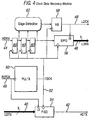
- FIG. 4 shows in more detail a CDRM 10, 22.
- the module 10, 22 has two primary functions. In transmit, it takes Low Speed Parallel Data (LDTX) on line 40 and creates High Speed Serial Data (HDTX) on line 42. In receive, it operates in reverse, taking High Speed Serial Data (HDRX) on line 44 and creating Low Speed Parallel Data (LDRX) on line 46. In addition, the receive operation also recovers a Low Speed Clock (LDCK) on line 48 from the serial data, that is phase aligned with the LDRX data. A Reference System Clock (REFCK) on line 49 is applied to a Phase Locked Loop 50 which multiplies the clock rate by a factor of 8 to provide a High Speed Clock (HSCK) on line 52.
- LDTX Low Speed Parallel Data
- HDTX High Speed Serial Data
- HDRX High Speed Serial Data
- LDRX Low Speed Parallel Data
- REFCK Reference System Clock
- HSCK High Speed Clock
- HSCK is applied to a parallel to serial register 54 and to a serial to parallel register 56.
- HSCK is also applied to a divide by 8 unit 58 and a chain of three toggles 60.
- the outputs of toggles 60 are detected by an edge detector device 62 which provides an output to divider unit 58.
- the output of divider unit 58 comprises the Low Speed Clock (LDCK) on line 48.
- LDCK Low Speed Clock
- LDTX Low Speed Data
- REFCK Reference Clock
- PLL Phase Locked Loop
- HSCK High Speed Clock
- PISO Parallel Serial Output
- the High Speed Clock (HSCK) will be divided by eight at 58 to create a Low Speed Clock (LDCK) output.
- the phase of this clock must be adjusted so that its associated Low Speed Data (LDRX) is stable at the time of the active edge of LDCK. This is done by edge detection and phase adjustment circuit 60, 62 which monitors the High Speed Data (HDRX) on line 44.
- HDRX is also passed into a Serial Parallel Output (SIPO) register 56 to create the Low Speed Received Parallel Data (LDRX) on line 46.
- SIPO Serial Parallel Output
- the number of transmit and sub-links are replicated 8 times in this example. However, there will generally only be a single PLL per CDRM macrocell.
- the serial links are passed through CDRM macrocell 22, and a W bit word and clock will be recovered for each of the N serial links.
- the CDRM 22 has no knowledge of the boundary between one W bit word and the next within the serial data stream and it is therefore the first task of the Interface 20 to identify the correct bit alignment within each sub-link. Having recovered the W bit words for each sub-link, all N of the W bit words have to be aligned and synchronised to recreate the original DW width word.
- the initialisation word is sent at least twice followed by another synchronisation word (user defined) delimiter to indicate the start of transmission of true data.
- the position of the word is located in the register by means of a state machine (not shown) and this information is relayed to subsequent stages.
- each ASIC transmitting/receiving interface will respectively create/recreate a CRC from the true data.
- the CRC words are inserted at a pre-determined interval, programmed to both transmit and receive sides. After this interval the transmitted CRC should equal the recreated CRC. If not, then either bit alignment has been lost or a corruption has occurred during the transmission of the data. This provides an Integrity Check individually on each of the serial links.
- the parallel words are placed in a bit alignment register 24 in each sub-link for detecting bit alignment. This is effected by a state machine (not shown) locking onto the position of the initialisation word within the register, and passing the bit aligned word to the next stage. In the next stage, an Integrity Check is performed on the CRC word at 26.
- the bit alignment and the Integrity Check are performed in each sub-link using the recovered clock generated for that serial link.
- the recovered clock generated for that serial link There is no guarantee of any phase relationship between any of the N recovered clock (RCK[n])s, and each of the recovered clocks may be jittering (except that the recovered clocks will be within one clock cycle of one another).
- the average frequency of all recovered clocks and that of the Transfer Clock, CK, on the transmit side must be exactly the same, since the reference clock to both the transmit and receive ASICs will be driven from the same crystal oscillator.
- a mechanism is therefore required to re-align the N recovered sub-words and resynchronise the wide data word back to the Transfer Clock, CK. This is done by using a short First In First Out (FIFO) 28, 6 words long, at the end of each serial link
- FIFO First In First Out
- the recovered sub-word plus a marker bit (W + 1 bits) is written to the FIFO 28 by its associated recovered clock on line 48.
- the marker bit indicates whether that data word was Transmitted Synchronisation or integrity Check Word.
- the very first word to be written by each of the links will be a synchronisation word (marker bit set) and the second will be the first sub-word of true data.
- the first write will occur at a slightly different time for each link, but by the time the second write occurs, all will have written at least once.
- the addressing of the FIFOs use Johnson coding, as more clearly seen in Figure 3.
- An address generator 32 provides a Johnson scheme of addressing to the write read address 34 of the respective FIFO 28.
- the initial value of the address is 011 and the address scheme changes as indicated in Figure 3.
- the most significant bit of the addresses of the sub-links are coupled by lines 36 to an OR gate 38.
- the output of the OR gate 38 is coupled by two metastability registers 70 to provide a trigger signal on line 72 to a state machine 74.
- State machine 74 provides an output on line 76 to control the reading out of the FIFO registers 28.
- the very first FIFO read will all be synchronised sub-words but the second will be the recovery of the first true wide data word.
- the output of the FIFOs are applied to a Word Aligner register 78 which reconstitutes the original data word 80 ( Figure 2 ).
- Word Alignment is checked at the same programmed interval used by the bit alignment, because at this time, and only at this time, all of the marker bits in each of the N FIFO's will be set.
- the scheme outlined provides a robust high speed, high bandwidth local link by using a number of serial asynchronous links in parallel.
Landscapes
- Engineering & Computer Science (AREA)
- General Engineering & Computer Science (AREA)
- Theoretical Computer Science (AREA)
- Computer Hardware Design (AREA)
- Physics & Mathematics (AREA)
- General Physics & Mathematics (AREA)
- Power Engineering (AREA)
- Computer Networks & Wireless Communication (AREA)
- Signal Processing (AREA)
- Communication Control (AREA)
- Synchronisation In Digital Transmission Systems (AREA)
Abstract
Description
- BW = Bandwidth in Mega bits per second (Mbps)
- CK = Transfer Clock in Mega Hertz (MHz)
| Previous & Current Word | Bit Alignment |
| 10111000xxxxxxxx | 0 |
| | 1 |
| | 2 |
| xxx10111000xxxxx | 3 |
| xxxx10111000xxxx | 4 |
| xxxxx10111000xxx | 5 |
| | 6 |
| xxxxxxx10111000x | 7 |
Claims (12)
- A data communication link for connecting first and second devices which have a system clock, the link including transmitting means for dividing an input word into a predetermined number of smaller words, and for providing a transfer clock having a high rate relative to the system clock, and including a predetermined number of sub-links, for transmitting a respective smaller word in serial form at the transfer clock rate, and means for receiving the serial words and for converting the serial words to a parallel form, including word alignment means, responsive to the system clock, for aligning said smaller words to reconstitute the input word.
- A link according to claim 1, wherein the first and second devices each comprise an ASIC device, the transmitting means comprising an interface of the first ASIC device and the receiving means comprising an interface of the second ASIC device.
- A device according to claim 1 or 2, wherein the means for transmitting comprises a parallel to serial register, and including means for generating the transfer clock coupled to the serial to parallel register for clocking serial words out of the register.
- A communication link according to any preceding claim, including transfer clock generating means comprising a Phased Locked Loop for receiving as an input the system clock.
- A communication link according to any preceding claim, wherein the receiving means for each sub-link comprises a serial to parallel register for receiving incoming serial words and converting them to parallel form, and means for generating a low speed clock from the incoming data with a frequency nominally equal to the system clock frequency.
- A data communication link according to claim 5, wherein the low speed clock generating means includes edge detection means for detecting incoming data and for providing an output to a dividing means for aligning the low speed clock with recovered data and for applying the same to the serial to parallel register for clocking out parallel words from the register.
- A data communication link according to any preceding claim, wherein the transmitting means includes means for generating bit alignment words, and the receiving means includes a bit alignment register for storing the bit alignment words in order to locate the position of the bits in the register.
- A data communication link according to any preceding claim, wherein the receiving means includes means for generating a cyclic redundancy code word and for transmitting the same at intervals, and the receiving means including check means for checking the cyclic redundancy code word.
- A data communication link according to any preceding claim, including a buffer memory in each sub-link for storing a predetermined number of received words, and means for reading the buffer memories in synchronism under control of the system clock in order to reconstitute the input data word.
- A data communication link according to claim 9, wherein the buffer memories each comprises a FIFO register.
- A data communication link according to claim 10, wherein the FIFO registers are addressed by an addressing scheme wherein only one bit of the address changes for incremental addresses.
- A data communication link according to claim 11, wherein a predetermined bit of the address of each FIFO are compared and employed to generate a trigger signal for actuating a state machine to cause reading of the FIFO registers.
Applications Claiming Priority (2)
| Application Number | Priority Date | Filing Date | Title |
|---|---|---|---|
| GBGB0006291.9A GB0006291D0 (en) | 2000-03-15 | 2000-03-15 | Data communication link |
| GB0006291 | 2000-03-15 |
Publications (3)
| Publication Number | Publication Date |
|---|---|
| EP1134668A2 true EP1134668A2 (en) | 2001-09-19 |
| EP1134668A3 EP1134668A3 (en) | 2006-02-08 |
| EP1134668B1 EP1134668B1 (en) | 2008-10-08 |
Family
ID=9887706
Family Applications (1)
| Application Number | Title | Priority Date | Filing Date |
|---|---|---|---|
| EP01300531A Expired - Lifetime EP1134668B1 (en) | 2000-03-15 | 2001-01-22 | Data communication link between two ASICs |
Country Status (4)
| Country | Link |
|---|---|
| US (2) | US7031347B2 (en) |
| EP (1) | EP1134668B1 (en) |
| DE (1) | DE60136025D1 (en) |
| GB (1) | GB0006291D0 (en) |
Cited By (8)
| Publication number | Priority date | Publication date | Assignee | Title |
|---|---|---|---|---|
| US6873939B1 (en) | 2001-02-02 | 2005-03-29 | Rambus Inc. | Method and apparatus for evaluating and calibrating a signaling system |
| EP1670199A1 (en) * | 2004-12-13 | 2006-06-14 | Altera Corporation | Design of channel alignment, error handling, and clock routing using hard-wired blocks for data transmission within programmable logic integrated circuits |
| US7137048B2 (en) | 2001-02-02 | 2006-11-14 | Rambus Inc. | Method and apparatus for evaluating and optimizing a signaling system |
| US7336749B2 (en) | 2004-05-18 | 2008-02-26 | Rambus Inc. | Statistical margin test methods and circuits |
| US7627029B2 (en) | 2003-05-20 | 2009-12-01 | Rambus Inc. | Margin test methods and circuits |
| US7765074B2 (en) | 2003-02-11 | 2010-07-27 | Rambus Inc. | Circuit, apparatus and method for capturing a representation of a waveform from a clock-data recovery (CDR) unit |
| GB2442501B (en) * | 2006-10-05 | 2011-04-13 | Advanced Risc Mach Ltd | Apparatus and method for data processing having an on-chip or off-chip interconnect between two or more devices |
| US8069378B2 (en) | 2001-02-02 | 2011-11-29 | Rambus Inc. | Method and apparatus for evaluating and optimizing a signaling system |
Families Citing this family (13)
| Publication number | Priority date | Publication date | Assignee | Title |
|---|---|---|---|---|
| US7231558B2 (en) | 2002-03-18 | 2007-06-12 | Finisar Corporation | System and method for network error rate testing |
| US7032139B1 (en) * | 2002-03-18 | 2006-04-18 | Finisar Corporation | Bit error rate tester |
| JP4407104B2 (en) * | 2002-08-30 | 2010-02-03 | 富士ゼロックス株式会社 | Signal transmission system |
| US8572289B1 (en) * | 2003-12-19 | 2013-10-29 | Nvidia Corporation | System, method and computer program product for stateless offloading of upper level network protocol operations |
| TWI254210B (en) * | 2004-05-26 | 2006-05-01 | Benq Corp | Serial transmission control system for accessing data based on status signal, system capable of multiplex controlling to output at different times, and printer and control method thereof |
| US7936793B2 (en) * | 2005-04-01 | 2011-05-03 | Freescale Semiconductor, Inc. | Methods and apparatus for synchronizing data transferred across a multi-pin asynchronous serial interface |
| US7953162B2 (en) * | 2006-11-17 | 2011-05-31 | Intersil Americas Inc. | Use of differential pair as single-ended data paths to transport low speed data |
| JP4336860B2 (en) * | 2007-02-21 | 2009-09-30 | 日本電気株式会社 | Serial interface circuit and serial receiver |
| US20100262887A1 (en) * | 2009-04-13 | 2010-10-14 | Lockheed Martin Corporation | High Integrity Data Network System and Method |
| US8627156B1 (en) * | 2010-10-26 | 2014-01-07 | Agilent Technologies, Inc. | Method and system of testing bit error rate using signal with mixture of scrambled and unscrambled bits |
| JP7041125B6 (en) * | 2016-09-02 | 2022-05-30 | コーニンクレッカ フィリップス エヌ ヴェ | Ultrasonic probe including low frequency low voltage digital microbeam former |
| US12495042B2 (en) * | 2021-08-16 | 2025-12-09 | Capital One Services, Llc | Systems and methods for resetting an authentication counter |
| US12119335B2 (en) | 2021-12-16 | 2024-10-15 | International Business Machines Corporation | Interconnection structures for high bandwidth data transfer |
Family Cites Families (22)
| Publication number | Priority date | Publication date | Assignee | Title |
|---|---|---|---|---|
| US3811014A (en) * | 1973-03-12 | 1974-05-14 | Logicon Inc | Adaptive pulse code modulation system |
| US5175727A (en) * | 1990-04-16 | 1992-12-29 | Maher John W | Communication system network interconnecting a plurality of communication systems |
| US5228056A (en) * | 1990-12-14 | 1993-07-13 | Interdigital Technology Corporation | Synchronous spread-spectrum communications system and method |
| JP3158213B2 (en) | 1991-09-12 | 2001-04-23 | 富士通株式会社 | Parallel transmission method and apparatus |
| JP3192030B2 (en) * | 1993-06-08 | 2001-07-23 | 富士通株式会社 | Interface device and communication system |
| US5522088A (en) * | 1994-06-17 | 1996-05-28 | International Business Machines Corporation | Shared channel subsystem has a self timed interface using a received clock signal to individually phase align bits received from a parallel bus |
| US5570356A (en) * | 1995-06-07 | 1996-10-29 | International Business Machines Corporation | High bandwidth communications system having multiple serial links |
| US5751724A (en) * | 1996-02-23 | 1998-05-12 | Dsc Communications Corporation | Demultiplexer for a multi-bitline bus |
| US6072781A (en) * | 1996-10-22 | 2000-06-06 | International Business Machines Corporation | Multi-tasking adapter for parallel network applications |
| US6150922A (en) * | 1997-01-23 | 2000-11-21 | Lucent Technologies Inc. | Serial communication technique |
| US6202108B1 (en) * | 1997-03-13 | 2001-03-13 | Bull S.A. | Process and system for initializing a serial link between two integrated circuits comprising a parallel-serial port using two clocks with different frequencies |
| US6167077A (en) * | 1997-12-23 | 2000-12-26 | Lsi Logic Corporation | Using multiple high speed serial lines to transmit high data rates while compensating for overall skew |
| US6594275B1 (en) * | 1998-04-03 | 2003-07-15 | Texas Instruments Incorporated | Fibre channel host bus adapter having multi-frequency clock buffer for reduced power consumption |
| US6201829B1 (en) * | 1998-04-03 | 2001-03-13 | Adaptec, Inc. | Serial/parallel GHZ transceiver with pseudo-random built in self test pattern generator |
| US6377575B1 (en) * | 1998-08-05 | 2002-04-23 | Vitesse Semiconductor Corporation | High speed cross point switch routing circuit with word-synchronous serial back plane |
| EP0996262A1 (en) | 1998-10-22 | 2000-04-26 | Texas Instruments France | Communication system with plurality of synchronised data links |
| US6618395B1 (en) | 1999-05-27 | 2003-09-09 | 3Com Corporation | Physical coding sub-layer for transmission of data over multi-channel media |
| US6140926A (en) * | 1999-07-21 | 2000-10-31 | Hewlett-Packard Company | Redundant status indicators for fault tolerance |
| US6775328B1 (en) * | 1999-08-11 | 2004-08-10 | Rambus Inc. | High-speed communication system with a feedback synchronization loop |
| US6577649B1 (en) * | 1999-11-12 | 2003-06-10 | International Business Machines Corporation | Multiplexer for asynchronous data |
| US6738935B1 (en) * | 2000-02-07 | 2004-05-18 | 3Com Corporation | Coding sublayer for multi-channel media with error correction |
| JP4407104B2 (en) * | 2002-08-30 | 2010-02-03 | 富士ゼロックス株式会社 | Signal transmission system |
-
2000
- 2000-03-15 GB GBGB0006291.9A patent/GB0006291D0/en not_active Ceased
-
2001
- 2001-01-22 EP EP01300531A patent/EP1134668B1/en not_active Expired - Lifetime
- 2001-01-22 DE DE60136025T patent/DE60136025D1/en not_active Expired - Lifetime
- 2001-03-15 US US09/808,664 patent/US7031347B2/en not_active Expired - Fee Related
-
2006
- 2006-03-22 US US11/386,418 patent/US20060187968A1/en not_active Abandoned
Cited By (24)
| Publication number | Priority date | Publication date | Assignee | Title |
|---|---|---|---|---|
| US8069378B2 (en) | 2001-02-02 | 2011-11-29 | Rambus Inc. | Method and apparatus for evaluating and optimizing a signaling system |
| US10855413B2 (en) | 2001-02-02 | 2020-12-01 | Rambus Inc. | Method and apparatus for evaluating and optimizing a signaling system |
| US7137048B2 (en) | 2001-02-02 | 2006-11-14 | Rambus Inc. | Method and apparatus for evaluating and optimizing a signaling system |
| US9356743B2 (en) | 2001-02-02 | 2016-05-31 | Rambus Inc. | Method and apparatus for evaluating and optimizing a signaling system |
| US7360127B2 (en) | 2001-02-02 | 2008-04-15 | Rambus Inc. | Method and apparatus for evaluating and optimizing a signaling system |
| US8812919B2 (en) | 2001-02-02 | 2014-08-19 | Rambus Inc. | Method and apparatus for evaluating and optimizing a signaling system |
| US6873939B1 (en) | 2001-02-02 | 2005-03-29 | Rambus Inc. | Method and apparatus for evaluating and calibrating a signaling system |
| US8812918B2 (en) | 2001-02-02 | 2014-08-19 | Rambus Inc. | Method and apparatus for evaluating and optimizing a signaling system |
| US8756469B2 (en) | 2001-02-02 | 2014-06-17 | Rambus Inc. | Method and apparatus for evaluating and optimizing a signaling system |
| US7765074B2 (en) | 2003-02-11 | 2010-07-27 | Rambus Inc. | Circuit, apparatus and method for capturing a representation of a waveform from a clock-data recovery (CDR) unit |
| US7627029B2 (en) | 2003-05-20 | 2009-12-01 | Rambus Inc. | Margin test methods and circuits |
| US10193642B2 (en) | 2003-05-20 | 2019-01-29 | Rambus Inc. | Margin test methods and circuits |
| US11233589B2 (en) | 2003-05-20 | 2022-01-25 | Rambus Inc. | Margin test methods and circuits |
| US10880022B1 (en) | 2003-05-20 | 2020-12-29 | Rambus Inc. | Margin test methods and circuits |
| US10735116B2 (en) | 2003-05-20 | 2020-08-04 | Rambus Inc. | Margin test methods and circuits |
| US8817932B2 (en) | 2003-05-20 | 2014-08-26 | Rambus Inc. | Margin test methods and circuits |
| US9116810B2 (en) | 2003-05-20 | 2015-08-25 | Rambus Inc. | Margin test methods and circuits |
| US8385492B2 (en) | 2003-05-20 | 2013-02-26 | Rambus Inc. | Receiver circuit architectures |
| US9544071B2 (en) | 2003-05-20 | 2017-01-10 | Rambus Inc. | Margin test methods and circuits |
| US7336749B2 (en) | 2004-05-18 | 2008-02-26 | Rambus Inc. | Statistical margin test methods and circuits |
| US7434192B2 (en) | 2004-12-13 | 2008-10-07 | Altera Corporation | Techniques for optimizing design of a hard intellectual property block for data transmission |
| EP1670199A1 (en) * | 2004-12-13 | 2006-06-14 | Altera Corporation | Design of channel alignment, error handling, and clock routing using hard-wired blocks for data transmission within programmable logic integrated circuits |
| GB2442501B (en) * | 2006-10-05 | 2011-04-13 | Advanced Risc Mach Ltd | Apparatus and method for data processing having an on-chip or off-chip interconnect between two or more devices |
| US8006008B2 (en) | 2006-10-05 | 2011-08-23 | Arm Limited | Apparatus and method for data processing having an on-chip or off-chip interconnect between two or more devices |
Also Published As
| Publication number | Publication date |
|---|---|
| US7031347B2 (en) | 2006-04-18 |
| US20060187968A1 (en) | 2006-08-24 |
| US20010033568A1 (en) | 2001-10-25 |
| GB0006291D0 (en) | 2000-05-03 |
| EP1134668A3 (en) | 2006-02-08 |
| DE60136025D1 (en) | 2008-11-20 |
| EP1134668B1 (en) | 2008-10-08 |
Similar Documents
| Publication | Publication Date | Title |
|---|---|---|
| EP1134668B1 (en) | Data communication link between two ASICs | |
| EP0424774B1 (en) | Clock distribution system and technique | |
| US6671753B2 (en) | Elastic interface apparatus and method therefor | |
| US6748039B1 (en) | System and method for synchronizing a skip pattern and initializing a clock forwarding interface in a multiple-clock system | |
| US5003558A (en) | Data synchronizing buffers for data processing channels | |
| US6792003B1 (en) | Method and apparatus for transporting and aligning data across multiple serial data streams | |
| US8520464B2 (en) | Interface circuit and semiconductor device incorporating same | |
| JPH05289770A (en) | Method and device for synchronization | |
| US5610953A (en) | Asynchronous low latency data recovery apparatus and method | |
| US6249875B1 (en) | Interface circuit using plurality of synchronizers for synchronizing respective control signals over a multi-clock environment | |
| US6356557B1 (en) | Hot insertable UTOPIA interface with automatic protection switching for backplane applications | |
| US8194652B2 (en) | Serializer for generating serial clock based on independent clock source and method for serial data transmission | |
| US5526360A (en) | High speed N-to-1 burst time-multiplexed data transmission system and method | |
| US20070300095A1 (en) | Double Data Rate Chaining for Synchronous DDR Interfaces | |
| EP0379279A2 (en) | Data transmission synchroniser | |
| US6640277B1 (en) | Input staging logic for latching source synchronous data | |
| US6341326B1 (en) | Method and apparatus for data capture using latches, delays, parallelism, and synchronization | |
| EP1317085B1 (en) | A method and circuit for initializing a de-skewing buffer in a clock forwarded system | |
| US6775339B1 (en) | Circuit design for high-speed digital communication | |
| US6920578B1 (en) | Method and apparatus for transferring data between a slower clock domain and a faster clock domain in which one of the clock domains is bandwidth limited | |
| CN119357117B (en) | TDM-based signal compression transmission method and system | |
| JP2596336B2 (en) | Asynchronous digital communication device | |
| EP1911188B1 (en) | Asynchronous data buffer | |
| JP3463212B2 (en) | Data transmission device | |
| US6771669B1 (en) | Method and apparatus for remote memory clock synchronization for optimized leadoff performance |
Legal Events
| Date | Code | Title | Description |
|---|---|---|---|
| PUAI | Public reference made under article 153(3) epc to a published international application that has entered the european phase |
Free format text: ORIGINAL CODE: 0009012 |
|
| AK | Designated contracting states |
Kind code of ref document: A2 Designated state(s): AT BE CH CY DE DK ES FI FR GB GR IE IT LI LU MC NL PT SE TR |
|
| AX | Request for extension of the european patent |
Free format text: AL;LT;LV;MK;RO;SI |
|
| PUAL | Search report despatched |
Free format text: ORIGINAL CODE: 0009013 |
|
| RIC1 | Information provided on ipc code assigned before grant |
Ipc: G06F 13/40 20060101AFI20010717BHEP Ipc: H04L 25/14 20060101ALI20051212BHEP |
|
| AK | Designated contracting states |
Kind code of ref document: A3 Designated state(s): AT BE CH CY DE DK ES FI FR GB GR IE IT LI LU MC NL PT SE TR |
|
| AX | Request for extension of the european patent |
Extension state: AL LT LV MK RO SI |
|
| 17P | Request for examination filed |
Effective date: 20060804 |
|
| 17Q | First examination report despatched |
Effective date: 20060911 |
|
| AKX | Designation fees paid |
Designated state(s): DE ES FR GB IT SE |
|
| RBV | Designated contracting states (corrected) |
Designated state(s): DE FR GB |
|
| GRAP | Despatch of communication of intention to grant a patent |
Free format text: ORIGINAL CODE: EPIDOSNIGR1 |
|
| GRAS | Grant fee paid |
Free format text: ORIGINAL CODE: EPIDOSNIGR3 |
|
| GRAA | (expected) grant |
Free format text: ORIGINAL CODE: 0009210 |
|
| AK | Designated contracting states |
Kind code of ref document: B1 Designated state(s): DE FR GB |
|
| REG | Reference to a national code |
Ref country code: GB Ref legal event code: FG4D |
|
| REF | Corresponds to: |
Ref document number: 60136025 Country of ref document: DE Date of ref document: 20081120 Kind code of ref document: P |
|
| PGFP | Annual fee paid to national office [announced via postgrant information from national office to epo] |
Ref country code: GB Payment date: 20090122 Year of fee payment: 9 |
|
| PLBE | No opposition filed within time limit |
Free format text: ORIGINAL CODE: 0009261 |
|
| STAA | Information on the status of an ep patent application or granted ep patent |
Free format text: STATUS: NO OPPOSITION FILED WITHIN TIME LIMIT |
|
| RAP4 | Party data changed (patent owner data changed or rights of a patent transferred) |
Owner name: LUCENT TECHNOLOGIES INC. |
|
| 26N | No opposition filed |
Effective date: 20090709 |
|
| GBPC | Gb: european patent ceased through non-payment of renewal fee |
Effective date: 20100122 |
|
| PG25 | Lapsed in a contracting state [announced via postgrant information from national office to epo] |
Ref country code: GB Free format text: LAPSE BECAUSE OF NON-PAYMENT OF DUE FEES Effective date: 20100122 |
|
| PGFP | Annual fee paid to national office [announced via postgrant information from national office to epo] |
Ref country code: FR Payment date: 20140108 Year of fee payment: 14 |
|
| REG | Reference to a national code |
Ref country code: DE Ref legal event code: R082 Ref document number: 60136025 Country of ref document: DE Representative=s name: DILG HAEUSLER SCHINDELMANN PATENTANWALTSGESELL, DE |
|
| REG | Reference to a national code |
Ref country code: FR Ref legal event code: ST Effective date: 20150930 |
|
| PG25 | Lapsed in a contracting state [announced via postgrant information from national office to epo] |
Ref country code: FR Free format text: LAPSE BECAUSE OF NON-PAYMENT OF DUE FEES Effective date: 20150202 |
|
| PGFP | Annual fee paid to national office [announced via postgrant information from national office to epo] |
Ref country code: DE Payment date: 20161219 Year of fee payment: 17 |
|
| REG | Reference to a national code |
Ref country code: DE Ref legal event code: R119 Ref document number: 60136025 Country of ref document: DE |
|
| PG25 | Lapsed in a contracting state [announced via postgrant information from national office to epo] |
Ref country code: DE Free format text: LAPSE BECAUSE OF NON-PAYMENT OF DUE FEES Effective date: 20180801 |
|
| REG | Reference to a national code |
Ref country code: DE Ref legal event code: R082 Ref document number: 60136025 Country of ref document: DE Representative=s name: DILG HAEUSLER SCHINDELMANN PATENTANWALTSGESELL, DE Ref country code: DE Ref legal event code: R081 Ref document number: 60136025 Country of ref document: DE Owner name: AVAGO TECHNOLOGIES GENERAL IP (SINGAPORE) PTE., SG Free format text: FORMER OWNER: LUCENT TECHNOLOGIES INC., MURRAY HILL, N.J., US |