EP1132964A2 - Wiring arrangement of power semiconductors in modules - Google Patents
Wiring arrangement of power semiconductors in modules Download PDFInfo
- Publication number
- EP1132964A2 EP1132964A2 EP01104998A EP01104998A EP1132964A2 EP 1132964 A2 EP1132964 A2 EP 1132964A2 EP 01104998 A EP01104998 A EP 01104998A EP 01104998 A EP01104998 A EP 01104998A EP 1132964 A2 EP1132964 A2 EP 1132964A2
- Authority
- EP
- European Patent Office
- Prior art keywords
- power semiconductor
- semiconductor chips
- module
- chips
- substrates
- Prior art date
- Legal status (The legal status is an assumption and is not a legal conclusion. Google has not performed a legal analysis and makes no representation as to the accuracy of the status listed.)
- Withdrawn
Links
Images
Classifications
-
- H—ELECTRICITY
- H01—ELECTRIC ELEMENTS
- H01L—SEMICONDUCTOR DEVICES NOT COVERED BY CLASS H10
- H01L25/00—Assemblies consisting of a plurality of individual semiconductor or other solid state devices ; Multistep manufacturing processes thereof
- H01L25/03—Assemblies consisting of a plurality of individual semiconductor or other solid state devices ; Multistep manufacturing processes thereof all the devices being of a type provided for in the same subgroup of groups H01L27/00 - H01L33/00, or in a single subclass of H10K, H10N, e.g. assemblies of rectifier diodes
- H01L25/04—Assemblies consisting of a plurality of individual semiconductor or other solid state devices ; Multistep manufacturing processes thereof all the devices being of a type provided for in the same subgroup of groups H01L27/00 - H01L33/00, or in a single subclass of H10K, H10N, e.g. assemblies of rectifier diodes the devices not having separate containers
- H01L25/07—Assemblies consisting of a plurality of individual semiconductor or other solid state devices ; Multistep manufacturing processes thereof all the devices being of a type provided for in the same subgroup of groups H01L27/00 - H01L33/00, or in a single subclass of H10K, H10N, e.g. assemblies of rectifier diodes the devices not having separate containers the devices being of a type provided for in group H01L29/00
- H01L25/072—Assemblies consisting of a plurality of individual semiconductor or other solid state devices ; Multistep manufacturing processes thereof all the devices being of a type provided for in the same subgroup of groups H01L27/00 - H01L33/00, or in a single subclass of H10K, H10N, e.g. assemblies of rectifier diodes the devices not having separate containers the devices being of a type provided for in group H01L29/00 the devices being arranged next to each other
-
- H—ELECTRICITY
- H01—ELECTRIC ELEMENTS
- H01L—SEMICONDUCTOR DEVICES NOT COVERED BY CLASS H10
- H01L2224/00—Indexing scheme for arrangements for connecting or disconnecting semiconductor or solid-state bodies and methods related thereto as covered by H01L24/00
- H01L2224/01—Means for bonding being attached to, or being formed on, the surface to be connected, e.g. chip-to-package, die-attach, "first-level" interconnects; Manufacturing methods related thereto
- H01L2224/42—Wire connectors; Manufacturing methods related thereto
- H01L2224/47—Structure, shape, material or disposition of the wire connectors after the connecting process
- H01L2224/48—Structure, shape, material or disposition of the wire connectors after the connecting process of an individual wire connector
- H01L2224/481—Disposition
- H01L2224/48151—Connecting between a semiconductor or solid-state body and an item not being a semiconductor or solid-state body, e.g. chip-to-substrate, chip-to-passive
- H01L2224/48221—Connecting between a semiconductor or solid-state body and an item not being a semiconductor or solid-state body, e.g. chip-to-substrate, chip-to-passive the body and the item being stacked
- H01L2224/48225—Connecting between a semiconductor or solid-state body and an item not being a semiconductor or solid-state body, e.g. chip-to-substrate, chip-to-passive the body and the item being stacked the item being non-metallic, e.g. insulating substrate with or without metallisation
- H01L2224/48227—Connecting between a semiconductor or solid-state body and an item not being a semiconductor or solid-state body, e.g. chip-to-substrate, chip-to-passive the body and the item being stacked the item being non-metallic, e.g. insulating substrate with or without metallisation connecting the wire to a bond pad of the item
-
- H—ELECTRICITY
- H01—ELECTRIC ELEMENTS
- H01L—SEMICONDUCTOR DEVICES NOT COVERED BY CLASS H10
- H01L2224/00—Indexing scheme for arrangements for connecting or disconnecting semiconductor or solid-state bodies and methods related thereto as covered by H01L24/00
- H01L2224/01—Means for bonding being attached to, or being formed on, the surface to be connected, e.g. chip-to-package, die-attach, "first-level" interconnects; Manufacturing methods related thereto
- H01L2224/42—Wire connectors; Manufacturing methods related thereto
- H01L2224/47—Structure, shape, material or disposition of the wire connectors after the connecting process
- H01L2224/49—Structure, shape, material or disposition of the wire connectors after the connecting process of a plurality of wire connectors
- H01L2224/491—Disposition
- H01L2224/4911—Disposition the connectors being bonded to at least one common bonding area, e.g. daisy chain
- H01L2224/49111—Disposition the connectors being bonded to at least one common bonding area, e.g. daisy chain the connectors connecting two common bonding areas, e.g. Litz or braid wires
-
- H—ELECTRICITY
- H01—ELECTRIC ELEMENTS
- H01L—SEMICONDUCTOR DEVICES NOT COVERED BY CLASS H10
- H01L2924/00—Indexing scheme for arrangements or methods for connecting or disconnecting semiconductor or solid-state bodies as covered by H01L24/00
- H01L2924/10—Details of semiconductor or other solid state devices to be connected
- H01L2924/11—Device type
- H01L2924/13—Discrete devices, e.g. 3 terminal devices
- H01L2924/1301—Thyristor
-
- H—ELECTRICITY
- H01—ELECTRIC ELEMENTS
- H01L—SEMICONDUCTOR DEVICES NOT COVERED BY CLASS H10
- H01L2924/00—Indexing scheme for arrangements or methods for connecting or disconnecting semiconductor or solid-state bodies as covered by H01L24/00
- H01L2924/10—Details of semiconductor or other solid state devices to be connected
- H01L2924/11—Device type
- H01L2924/13—Discrete devices, e.g. 3 terminal devices
- H01L2924/1304—Transistor
- H01L2924/1305—Bipolar Junction Transistor [BJT]
- H01L2924/13055—Insulated gate bipolar transistor [IGBT]
Definitions
- the present invention relates to an arrangement for interconnection of power semiconductor chips in modules where the power semiconductor chips at least two different ones Assigned function types and each via ceramic substrates are applied to a common base plate.
- IGBT bipolar transistor with isolated Gate
- IGBT bipolar transistor with isolated Gate
- DCB "sandwich substrate” copper-ceramic-copper.
- the ceramic substrates in turn are preferred soldered to a base plate.
- the ceramic substrate takes over in particular DCB, the function of an electrical one Isolation and thermal conduction in the power semiconductor chip arising heat. Also includes the ceramic substrate structures associated with bonded wires the electrical function of the power semiconductor chip realize.
- the base plate serves as a support mechanically and thermally as a heat capacity and heat conductor to one if necessary additionally provided heat sink on which the power semiconductor module is screwed.
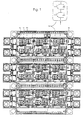
- IGBT power semiconductor chips and diode power semiconductor chips checkered pattern on the individual Substrates as well as overall on the bottom plate in the Module provided.
- Power semiconductor chips of the same Function types occupy fields of the same Color of the checkerboard pattern.
- IGBT power semiconductor chips are for example on "black” Fields provided while diode power semiconductor chips assigned to the "white” fields are.
- individual power semiconductor chips are in in the form of IGBT chips 1 and diode chips 2 over substrates 3 applied to a base plate 4 and in the manner of a checkerboard pattern arranged.
- substrates 3 preferably DCB used.
- Half bridges 4 Basic electrical functions are on the substrates 3 as Half bridges 4 realized and by means of a bus system 5 and corresponding bond wires connected in parallel to each other. To simplify the illustration, there are only one bus system at a time 5 and a half-bridge 4 particularly highlighted.
- individual substrates can be cut by current measuring resistors be replaced.
- additional functions that is, current measurements in, for example, linearly guided phase lines possible.
- Rectifier input bridges instead of individual substrates in the module can be installed.
Abstract
Description
Die vorliegende Erfindung betrifft eine Anordnung zur Verschaltung von Leistungshalbleiterchips in Modulen, bei der die Leistungshalbleiterchips wenigstens zwei verschiedenen Funktionstypen zugeordnet und jeweils über keramische Substrate auf eine gemeinsame Bodenplatte aufgebracht sind.The present invention relates to an arrangement for interconnection of power semiconductor chips in modules where the power semiconductor chips at least two different ones Assigned function types and each via ceramic substrates are applied to a common base plate.
In Leistungshalbleitermodulen sind bekanntlich elektronische Bauteile, wie insbesondere IGBT-Chips und Dioden-Chips miteinander verschaltet (IGBT = Bipolartransistor mit isoliertem Gate). Außer IGBT-Chips und Dioden-Chips können in solchen Leistungshalbleitermodulen auch andere elektronische Bauteile eingesetzt werden. Beispiele hierfür sind Leistungstransistoren, Thyristoren und so weiter.As is known, electronic power modules are used in power semiconductor modules Components, such as in particular IGBT chips and diode chips with one another interconnected (IGBT = bipolar transistor with isolated Gate). Except IGBT chips and diode chips can be used in such Power semiconductor modules also other electronic Components are used. Examples of this are power transistors, Thyristors and so on.
Die Leistungshalbleiterchips sind in solchen Leistungshalbleitermodulen auf keramischen Substraten, wie beispielsweise DCB aufgelötet (DCB = "Sandwichsubstrat" Kupfer-Keramik-Kupfer). Die keramischen Substrate ihrerseits sind vorzugsweise mit einer Bodenplatte verlötet.The power semiconductor chips are in such power semiconductor modules on ceramic substrates, such as DCB soldered (DCB = "sandwich substrate" copper-ceramic-copper). The ceramic substrates in turn are preferred soldered to a base plate.
Bei einer derartigen Anordnung übernimmt das keramische Substrat, also insbesondere DCB, die Funktion einer elektrischen Isolation und einer thermischen Leitung der im Leistungshalbleiterchip entstehenden Wärme. Außerdem beinhaltet das keramische Substrat Strukturen, die in Verbindung mit gebondeten Drähten die elektrische Funktion des Leistungshalbleiterchips verwirklichen.With such an arrangement, the ceramic substrate takes over in particular DCB, the function of an electrical one Isolation and thermal conduction in the power semiconductor chip arising heat. Also includes the ceramic substrate structures associated with bonded wires the electrical function of the power semiconductor chip realize.
Die Bodenplatte dient mechanisch als Träger sowie thermisch als Wärmekapazität und Wärmeleiter zu einem gegebenenfalls zusätzlich vorgesehenen Kühlkörper, auf welchen der Leistungshalbleitermodul geschraubt ist. The base plate serves as a support mechanically and thermally as a heat capacity and heat conductor to one if necessary additionally provided heat sink on which the power semiconductor module is screwed.
In einem solchen Leistungshalbleitermodul können, wenn hohe Leistungen zu verarbeiten sind, zahlreiche Leistungshalbleiterchips intern parallel zueinander geschaltet werden. Speziell bei einer solchen Parallelschaltung treten aber verschiedene Probleme auf, die im folgenden näher angegeben werden sollen:In such a power semiconductor module, if high Services to be processed, numerous power semiconductor chips internally connected in parallel to each other. Specifically with such a parallel connection, however, different Problems on specified below should be:
Räumlich eng nebeneinanderliegende bzw. benachbarte Leistungshalbleiterchips beeinflussen sich thermisch gegenseitig, was eine unkontrollierte Erwärmung des Moduls nach sich zieht und eine Abfuhr von Wärme bzw. Entwärmung des Moduls schwierig macht.Power semiconductor chips that are spatially closely adjacent or adjacent influence each other thermally, which results in an uncontrolled heating of the module pulls and dissipation of heat or cooling of the module makes difficult.
Lokale Wärmespitzen, die speziell bei unsymmetrischen Anordnungen der einzelnen Leistungshalbleiterchips auftreten, können statische und dynamische Fehlaufteilungen von Strömen im Modul sowie Schwingungserscheinungen nach sich ziehen.Local heat peaks, especially with asymmetrical arrangements of the individual power semiconductor chips occur, can static and dynamic misallocations of currents in the module as well as vibrations.
Schließlich werfen Funktionserweiterungen eines Moduls Probleme auf, wenn beispielsweise eine Grundfunktion, die von mehreren einzelnen Leistungshalbleiterchips ausgeübt wird, geändert werden soll; das heißt, die Flexibilität des Moduls ist eingeschränkt.Finally, functional extensions of a module pose problems when, for example, a basic function performed by several individual power semiconductor chips are exercised, to be changed; that is, the flexibility of the module is restricted.
Um die oben genannten Probleme zu vermeiden bzw. zu umgehen, wird bisher daran gedacht, die einzelnen Leistungshalbleiterchips direkt nebeneinander vorzusehen und dabei aber thermisch geringer zu beanspruchen, was aber aufwendige Kühlkonzepte notwendig macht. Eine andere Möglichkeit besteht darin, in einem Modul nur eine geringere Anzahl von Leistungshalbleiterchips zu integrieren, also einen größeren Platzbedarf in Kauf zu nehmen. Weiterhin können Fehlaufteilungen von Strömen oder Schwingungserscheinungen als unvermeidbar akzeptiert werden. Schließlich sind Funktionserweiterungen bzw. Änderungen einer Grundfunktion möglich, wenn das Layout des Moduls grundsätzlich entsprechend verändert wird, was praktisch einer Neukonstruktion des Moduls gleich kommt.To avoid or work around the above problems, So far, the individual power semiconductor chips have been considered to be provided directly next to each other and yet to be thermally less demanding, but this is expensive Makes cooling concepts necessary. Another option is there only a small number of in one module Integrate power semiconductor chips, so a larger one To accept space requirements. Furthermore, misallocations of currents or vibrations as inevitable be accepted. After all, there are functional extensions or changes to a basic function possible if the layout of the module changed accordingly becomes what is practically the same as a redesign of the module is coming.
Es gibt also bisher noch keine befriedigende Lösung der oben aufgezeigten Probleme.So there is still no satisfactory solution to the above identified problems.
Es ist daher Aufgabe der vorliegenden Erfindung, eine Anordnung zur Verschaltung von Leistungshalbleiterchips in Modulen anzugeben, bei der thermische Beeinflussungen der Leistungshalbleiterchips untereinander weitgehend ausgeschlossen sind, so daß auch keine statischen und dynamischen Fehlaufteilungen von Strömen auftreten, und bei der zusätzlich Funktionserweiterungen ohne grundsätzliche Änderung des Layouts des Moduls möglich sind.It is therefore an object of the present invention to provide an arrangement for connecting power semiconductor chips in modules to be specified in the case of thermal influences on the power semiconductor chips largely excluded from each other are, so that no static and dynamic misallocations of currents occur, and at the additional Functional extensions without a fundamental change in the layout of the module are possible.
Diese Aufgabe wird bei einer Anordnung der eingangs genannten Art erfindungsgemäß dadurch gelöst, daß die Leistungshalbleiterchips schachbrettmusterartig angeordnet sind und möglichst gleiche Funktionstypen Felder der gleichen Farbe des Schachbrettmusters besetzen.This object is achieved with an arrangement of the aforementioned Art solved according to the invention in that the power semiconductor chips are arranged in a checkerboard pattern and Function types that are the same if possible Fields of the same color of the checkerboard pattern.
Bei der erfindungsgemäßen Anordnung sind also beispielsweise IGBT-Leistungshalbleiterchips und Dioden-Leistungshalbleiterchips schachbrettmusterartig auf den einzelnen Substraten sowie insgesamt auf der Bodenplatte in dem Modul vorgesehen. Leistungshalbleiterchips der gleichen Funktionstypen belegen dabei jeweils Felder der gleichen Farbe des Schachbrettmusters. Mit anderen Worten, IGBT-Leistungshalbleiterchips werden beispielsweise auf "schwarzen" Feldern vorgesehen, während Dioden-Leistungshalbleiterchips den "weißen" Feldern zugewiesen sind.In the arrangement according to the invention, for example IGBT power semiconductor chips and diode power semiconductor chips checkered pattern on the individual Substrates as well as overall on the bottom plate in the Module provided. Power semiconductor chips of the same Function types occupy fields of the same Color of the checkerboard pattern. In other words, IGBT power semiconductor chips are for example on "black" Fields provided while diode power semiconductor chips assigned to the "white" fields are.
Durch diese Maßnahme überlappen sich die Wärmespreizungszonen der einzelnen Leistungshalbleiterchips nur minimal. Außerdem wird in vorteilhafter Weise ausgenutzt, daß Leistungshalbleiterchips mit unterschiedlicher Funktion, also beispielsweise IGBT-Leistungshalbleiterchips und Dioden-Leistungshalbleiterchips, in den unterschiedlichen Betriebszuständen des Moduls nicht zeitgleich ihre stärkste Erwärmung erfahren, so daß selbst eine gegebenenfalls auftretende Überlappung der Wärmespreizungszonen ohne negative Auswirkungen bleibt.This measure overlaps the heat spreading zones of the individual power semiconductor chips only minimal. Moreover is used in an advantageous manner that power semiconductor chips with different functions, so for example IGBT power semiconductor chips and diode power semiconductor chips, in the different operating states the module does not heat up at the same time experienced so that even a possibly occurring Overlap of the heat spreading zones without negative effects remains.
Die Realisierung einer elektrischen Grundfunktion als Halbbrücke auf nur einem Substrat, insbesondere DCB, führt zu einer räumlichen Trennung parallelgeschalteter Leistungshalbleiterchips auf benachbarten Substraten, so daß auch hier keine Überlappungen von Wärmespreizzonen zu erwarten sind.The realization of an electrical basic function as a half bridge on just one substrate, especially DCB, leads to a spatial separation of power semiconductor chips connected in parallel on neighboring substrates, so that too no overlaps of heat spreading zones are to be expected here are.
Durch die bereits erwähnte Realisierung einer elektrischen Grundfunktion als Halbbrücke auf einem Substrat wird durch entsprechende Strukturierung eines Bussystems eine symmetrische Parallelschaltung der Grundfunktionen durch Bonddrähte möglich. Diese symmetrische Anordnung, deren Symmetrie sich auch auf weitere Leitungen, wie insbesondere Steuerleitungen bezieht, wird im Modul mehrfach dupliziert angewendet.Through the already mentioned realization of an electrical Basic function as a half bridge on a substrate is performed by appropriate structuring of a bus system a symmetrical Parallel connection of the basic functions through bond wires possible. This symmetrical arrangement, the symmetry of which also on other lines, such as control lines in particular is used, duplicated in the module.
Da schließlich die Grundfunktion auf einem Substrat realisiert ist, kann ein parallel geschaltetes Substrat durch eine andere Funktion ersetzt werden, ohne das Grundkonzept des Moduls neu aufzubauen und zu verändern. Diese Flexibilität wird durch die bereits erwähnte Symmetrie des Bussystems gefördert.Because the basic function is finally realized on a substrate is a substrate connected in parallel by a other function can be replaced without the basic concept of Rebuild and change module. This flexibility is promoted by the symmetry of the bus system already mentioned.
Nachfolgend wird die Erfindung anhand der Zeichnung näher erläutert, in deren einziger Figur eine schematische Draufsicht auf einen Modul gezeigt ist.The invention will be described in more detail below with the aid of the drawing explained, in their single figure a schematic plan view is shown on a module.
In diesem Modul sind einzelne Leistungshalbleiterchips in der Form von IGBT-Chips 1 und Dioden-Chips 2 über Substrate 3 auf einer Grundplatte 4 aufgebracht und dabei schachbrettmusterartig angeordnet. Für die Substrate 3 wird dabei in bevorzugter Weise DCB verwendet.In this module, individual power semiconductor chips are in in the form of IGBT chips 1 and diode chips 2 over substrates 3 applied to a base plate 4 and in the manner of a checkerboard pattern arranged. For the substrates 3, preferably DCB used.
Auf den Substraten 3 sind elektrische Grundfunktionen als Halbbrücken 4 realisiert und mittels eines Bussystems 5 und entsprechenden Bonddrähten parallel zueinander geschaltet. Zur Vereinfachung der Darstellung sind jeweils nur ein Bussystem 5 und eine Halbbrücke 4 besonders herausgestellt.Basic electrical functions are on the substrates 3 as Half bridges 4 realized and by means of a bus system 5 and corresponding bond wires connected in parallel to each other. To simplify the illustration, there are only one bus system at a time 5 and a half-bridge 4 particularly highlighted.
Durch die schachbrettmusterartige Anordnung der einzelnen Leistungshalbleiterchips wird erreicht, daß Überlappungen von Wärmespreizungszonen nur minimal sind. Außerdem wird in vorteilhafter Weise ausgenutzt, daß Leistungshalbleiterchips mit unterschiedlicher Funktion, also die IGBT-Chips 1 und die Dioden-Chips 2 in den unterschiedlichen Betriebszuständen des Moduls nicht zeitgleich ihre stärkste Erwärmung erfahren, so daß die zeitverschobene Überlappung der Wärmespreizungszonen ohne negative Auswirkungen bleibt.Due to the checkered pattern arrangement of the individual Power semiconductor chips is achieved that overlaps of heat spreading zones are minimal. In addition, in exploited advantageously that power semiconductor chips with different functions, i.e. the IGBT chips 1 and the diode chips 2 in the different operating states the module does not experience its greatest warming at the same time, so that the time-shifted overlap of the heat spreading zones remains without negative effects.
Wesentlich an der vorliegenden Erfindung ist also die schachbrettmusterartige Anordnung von beispielsweise IGBT-Chips und Dioden-Chips in einem Modul, wobei funktionsgleiche Chips jeweils Felder der gleichen Farbe belegen. Bei einer derartigen Anordnung der verschiedenen Chips in einem Schachbrettmuster kann die Busstruktur ohne weiteres linear entlang der einzelnen Chips geführt werden. Elektrische Grundfunktionen lassen sich ohne weiteres auf einzelnen Substraten realisieren, wodurch eine Erweiterung durch identische Substrate möglich ist, um durch Parallelschaltung eine Leistungssteigerung zu erzielen. Ebenso kann eine Erweiterung durch abweichende Substrate vorgenommen werden, um zu einer Veränderung der Funktion des Moduls insgesamt zu gelangen.What is essential to the present invention is that Checkerboard-like arrangement of IGBT chips, for example and diode chips in one module, with the same function Chips occupy fields of the same color. At a such arrangement of the various chips in one Checkerboard patterns can easily make the bus structure linear are routed along the individual chips. Electrical Basic functions can easily be performed on individual substrates realize, thereby expanding through identical Substrates is possible to by a parallel connection Achieve performance improvement. An extension can also be used through different substrates to be made a change in the function of the module as a whole.
So können beispielsweise einzelne Substrate durch Strom-Meßwiderstände ersetzt werden. Hiermit sind Zusatzfunktionen, also Strommessungen in beispielsweise linear geführten Phasenleitungen möglich. Ebenso können auch beispielsweise Gleichrichtereingangsbrücken anstelle einzelner Substrate in den Modul eingebaut werden.For example, individual substrates can be cut by current measuring resistors be replaced. Hereby are additional functions, that is, current measurements in, for example, linearly guided phase lines possible. Likewise, for example Rectifier input bridges instead of individual substrates in the module can be installed.
Claims (3)
dadurch gekennzeichnet, daß
characterized in that
dadurch gekennzeichnet, daß
die Funktionstypen durch IGBT's und Leistungsdioden gegeben sind.Arrangement according to claim 1,
characterized in that
the function types are given by IGBTs and power diodes.
dadurch gekennzeichnet, daß
Grundfunktionen des Moduls auf jeweils einem der Substrate (3) realisiert sind.Arrangement according to claim 1 or 2,
characterized in that
Basic functions of the module are implemented on one of the substrates (3).
Applications Claiming Priority (2)
| Application Number | Priority Date | Filing Date | Title |
|---|---|---|---|
| DE10011633A DE10011633A1 (en) | 2000-03-10 | 2000-03-10 | Arrangement for connecting power semiconductor chips in modules |
| DE10011633 | 2000-03-10 |
Publications (2)
| Publication Number | Publication Date |
|---|---|
| EP1132964A2 true EP1132964A2 (en) | 2001-09-12 |
| EP1132964A3 EP1132964A3 (en) | 2003-11-12 |
Family
ID=7634187
Family Applications (1)
| Application Number | Title | Priority Date | Filing Date |
|---|---|---|---|
| EP01104998A Withdrawn EP1132964A3 (en) | 2000-03-10 | 2001-03-01 | Wiring arrangement of power semiconductors in modules |
Country Status (3)
| Country | Link |
|---|---|
| US (1) | US20010026434A1 (en) |
| EP (1) | EP1132964A3 (en) |
| DE (1) | DE10011633A1 (en) |
Families Citing this family (7)
| Publication number | Priority date | Publication date | Assignee | Title |
|---|---|---|---|---|
| DE10316356B4 (en) | 2003-04-10 | 2012-07-26 | Semikron Elektronik Gmbh & Co. Kg | Modular power semiconductor module |
| DE10317018A1 (en) * | 2003-04-11 | 2004-11-18 | Infineon Technologies Ag | Multichip module with several semiconductor chips and printed circuit board with several components |
| SI2340560T1 (en) | 2008-01-25 | 2014-02-28 | Letrika Lab D.O.O. | Power switching module |
| DE112013001234B4 (en) | 2012-03-01 | 2023-02-02 | Mitsubishi Electric Corporation | Power semiconductor module and energy conversion device |
| DE102015103667A1 (en) * | 2015-03-12 | 2016-09-15 | Infineon Technologies Bipolar Gmbh & Co. Kg | Power semiconductor module with improved bond connection structure |
| CN113126703B (en) * | 2020-01-14 | 2023-09-08 | 戴尔产品有限公司 | Power transmission system |
| CN113270374A (en) * | 2021-04-30 | 2021-08-17 | 深圳芯能半导体技术有限公司 | IGBT power device |
Citations (4)
| Publication number | Priority date | Publication date | Assignee | Title |
|---|---|---|---|---|
| EP0499707A1 (en) * | 1991-02-22 | 1992-08-26 | Asea Brown Boveri Ag | Gate turn-off semiconductor power component |
| DE9313483U1 (en) * | 1993-09-07 | 1994-01-05 | Sze Microelectronics Gmbh | Recording device |
| EP0884781A2 (en) * | 1997-06-12 | 1998-12-16 | Hitachi, Ltd. | Power semiconductor module |
| JPH11103012A (en) * | 1997-09-29 | 1999-04-13 | Denso Corp | Inverter module for drive motor |
-
2000
- 2000-03-10 DE DE10011633A patent/DE10011633A1/en not_active Ceased
-
2001
- 2001-03-01 EP EP01104998A patent/EP1132964A3/en not_active Withdrawn
- 2001-03-12 US US09/803,759 patent/US20010026434A1/en not_active Abandoned
Patent Citations (4)
| Publication number | Priority date | Publication date | Assignee | Title |
|---|---|---|---|---|
| EP0499707A1 (en) * | 1991-02-22 | 1992-08-26 | Asea Brown Boveri Ag | Gate turn-off semiconductor power component |
| DE9313483U1 (en) * | 1993-09-07 | 1994-01-05 | Sze Microelectronics Gmbh | Recording device |
| EP0884781A2 (en) * | 1997-06-12 | 1998-12-16 | Hitachi, Ltd. | Power semiconductor module |
| JPH11103012A (en) * | 1997-09-29 | 1999-04-13 | Denso Corp | Inverter module for drive motor |
Non-Patent Citations (2)
| Title |
|---|
| BAYERER R ET AL: "LEISTUNGSHALBLEITERMODULE IN DIREKT-BONDING-TECHNIK" TECHNISCHE RUNDSCHAU, HALLWAG VERLAG. BERN, CH, Bd. 80, Nr. 32, 5. August 1988 (1988-08-05), Seiten 38-41,43,45, XP000110807 ISSN: 1023-0823 * |
| PATENT ABSTRACTS OF JAPAN vol. 1999, no. 09, 30. Juli 1999 (1999-07-30) -& JP 11 103012 A (DENSO CORP), 13. April 1999 (1999-04-13) * |
Also Published As
| Publication number | Publication date |
|---|---|
| US20010026434A1 (en) | 2001-10-04 |
| DE10011633A1 (en) | 2001-09-20 |
| EP1132964A3 (en) | 2003-11-12 |
Similar Documents
| Publication | Publication Date | Title |
|---|---|---|
| EP3942603B1 (en) | Electronic switching circuit and method for producing same | |
| DE19645636C1 (en) | Power module for operating electric motor with speed and power control | |
| DE10393437T5 (en) | Semiconductor device assembly | |
| DE19900603A1 (en) | Electronic semiconductor module | |
| DE102012219686B4 (en) | Power module with low leakage inductance | |
| DE102007013186A1 (en) | Semiconductor module with semiconductor chips and method for producing the same | |
| DE102007046969B3 (en) | Electronic circuit of subcircuits and method for their manufacture and the corresponding converter or switch | |
| DE102012213407A1 (en) | A semiconductor device | |
| DE102015101086B4 (en) | SEMICONDUCTOR POWER MODULE ARRANGEMENT | |
| DE102010002627A1 (en) | Low-inductance power semiconductor module | |
| EP1178595B1 (en) | Arrangement with a low inductance for circuit | |
| DE112016005574B4 (en) | semiconductor modules | |
| EP0750345B1 (en) | Power semiconductor module | |
| DE60317270T2 (en) | Semiconductor module and power converter | |
| DE102018112477A1 (en) | SEMICONDUCTOR PACKAGE WITH LADDER FRAME | |
| EP1083599A2 (en) | Power semiconductor module | |
| DE212020000459U1 (en) | Semiconductor component | |
| DE112020006374T5 (en) | Power module with improved electrical and thermal characteristics | |
| DE112020002901T5 (en) | POWER SEMICONDUCTOR MODULE | |
| DE60306040T2 (en) | Semiconductor module and power converter device | |
| DE102005049978A1 (en) | Circuit arrangement for buck-converter, has half-bridges accommodated in semiconductor housing | |
| EP1132964A2 (en) | Wiring arrangement of power semiconductors in modules | |
| EP0710983B1 (en) | Bridge module | |
| DE102018216399B4 (en) | Method for manufacturing a power semiconductor module and power semiconductor module | |
| EP3949103A1 (en) | Electronic circuit module |
Legal Events
| Date | Code | Title | Description |
|---|---|---|---|
| PUAI | Public reference made under article 153(3) epc to a published international application that has entered the european phase |
Free format text: ORIGINAL CODE: 0009012 |
|
| AK | Designated contracting states |
Kind code of ref document: A2 Designated state(s): AT BE CH CY DE DK ES FI FR GB GR IE IT LI LU MC NL PT SE TR |
|
| AX | Request for extension of the european patent |
Free format text: AL;LT;LV;MK;RO;SI |
|
| PUAL | Search report despatched |
Free format text: ORIGINAL CODE: 0009013 |
|
| AK | Designated contracting states |
Kind code of ref document: A3 Designated state(s): AT BE CH CY DE DK ES FI FR GB GR IE IT LI LU MC NL PT SE TR |
|
| AX | Request for extension of the european patent |
Extension state: AL LT LV MK RO SI |
|
| RIC1 | Information provided on ipc code assigned before grant |
Ipc: 7H 01L 25/11 B Ipc: 7H 01L 25/07 A |
|
| AKX | Designation fees paid | ||
| REG | Reference to a national code |
Ref country code: DE Ref legal event code: 8566 |
|
| STAA | Information on the status of an ep patent application or granted ep patent |
Free format text: STATUS: THE APPLICATION IS DEEMED TO BE WITHDRAWN |
|
| 18D | Application deemed to be withdrawn |
Effective date: 20040513 |