EP1132883A2 - Apparatus and method for controlling gray level for display panel - Google Patents
Apparatus and method for controlling gray level for display panel Download PDFInfo
- Publication number
- EP1132883A2 EP1132883A2 EP01302039A EP01302039A EP1132883A2 EP 1132883 A2 EP1132883 A2 EP 1132883A2 EP 01302039 A EP01302039 A EP 01302039A EP 01302039 A EP01302039 A EP 01302039A EP 1132883 A2 EP1132883 A2 EP 1132883A2
- Authority
- EP
- European Patent Office
- Prior art keywords
- bits
- display panel
- data
- gray level
- pulse
- Prior art date
- Legal status (The legal status is an assumption and is not a legal conclusion. Google has not performed a legal analysis and makes no representation as to the accuracy of the status listed.)
- Granted
Links
Images


Classifications
-
- G—PHYSICS
- G02—OPTICS
- G02F—OPTICAL DEVICES OR ARRANGEMENTS FOR THE CONTROL OF LIGHT BY MODIFICATION OF THE OPTICAL PROPERTIES OF THE MEDIA OF THE ELEMENTS INVOLVED THEREIN; NON-LINEAR OPTICS; FREQUENCY-CHANGING OF LIGHT; OPTICAL LOGIC ELEMENTS; OPTICAL ANALOGUE/DIGITAL CONVERTERS
- G02F1/00—Devices or arrangements for the control of the intensity, colour, phase, polarisation or direction of light arriving from an independent light source, e.g. switching, gating or modulating; Non-linear optics
- G02F1/01—Devices or arrangements for the control of the intensity, colour, phase, polarisation or direction of light arriving from an independent light source, e.g. switching, gating or modulating; Non-linear optics for the control of the intensity, phase, polarisation or colour
- G02F1/13—Devices or arrangements for the control of the intensity, colour, phase, polarisation or direction of light arriving from an independent light source, e.g. switching, gating or modulating; Non-linear optics for the control of the intensity, phase, polarisation or colour based on liquid crystals, e.g. single liquid crystal display cells
- G02F1/133—Constructional arrangements; Operation of liquid crystal cells; Circuit arrangements
-
- G—PHYSICS
- G09—EDUCATION; CRYPTOGRAPHY; DISPLAY; ADVERTISING; SEALS
- G09G—ARRANGEMENTS OR CIRCUITS FOR CONTROL OF INDICATING DEVICES USING STATIC MEANS TO PRESENT VARIABLE INFORMATION
- G09G3/00—Control arrangements or circuits, of interest only in connection with visual indicators other than cathode-ray tubes
- G09G3/20—Control arrangements or circuits, of interest only in connection with visual indicators other than cathode-ray tubes for presentation of an assembly of a number of characters, e.g. a page, by composing the assembly by combination of individual elements arranged in a matrix no fixed position being assigned to or needed to be assigned to the individual characters or partial characters
- G09G3/2007—Display of intermediate tones
- G09G3/2077—Display of intermediate tones by a combination of two or more gradation control methods
- G09G3/2081—Display of intermediate tones by a combination of two or more gradation control methods with combination of amplitude modulation and time modulation
-
- G—PHYSICS
- G09—EDUCATION; CRYPTOGRAPHY; DISPLAY; ADVERTISING; SEALS
- G09G—ARRANGEMENTS OR CIRCUITS FOR CONTROL OF INDICATING DEVICES USING STATIC MEANS TO PRESENT VARIABLE INFORMATION
- G09G3/00—Control arrangements or circuits, of interest only in connection with visual indicators other than cathode-ray tubes
- G09G3/20—Control arrangements or circuits, of interest only in connection with visual indicators other than cathode-ray tubes for presentation of an assembly of a number of characters, e.g. a page, by composing the assembly by combination of individual elements arranged in a matrix no fixed position being assigned to or needed to be assigned to the individual characters or partial characters
- G09G3/22—Control arrangements or circuits, of interest only in connection with visual indicators other than cathode-ray tubes for presentation of an assembly of a number of characters, e.g. a page, by composing the assembly by combination of individual elements arranged in a matrix no fixed position being assigned to or needed to be assigned to the individual characters or partial characters using controlled light sources
- G09G3/30—Control arrangements or circuits, of interest only in connection with visual indicators other than cathode-ray tubes for presentation of an assembly of a number of characters, e.g. a page, by composing the assembly by combination of individual elements arranged in a matrix no fixed position being assigned to or needed to be assigned to the individual characters or partial characters using controlled light sources using electroluminescent panels
- G09G3/32—Control arrangements or circuits, of interest only in connection with visual indicators other than cathode-ray tubes for presentation of an assembly of a number of characters, e.g. a page, by composing the assembly by combination of individual elements arranged in a matrix no fixed position being assigned to or needed to be assigned to the individual characters or partial characters using controlled light sources using electroluminescent panels semiconductive, e.g. using light-emitting diodes [LED]
- G09G3/3208—Control arrangements or circuits, of interest only in connection with visual indicators other than cathode-ray tubes for presentation of an assembly of a number of characters, e.g. a page, by composing the assembly by combination of individual elements arranged in a matrix no fixed position being assigned to or needed to be assigned to the individual characters or partial characters using controlled light sources using electroluminescent panels semiconductive, e.g. using light-emitting diodes [LED] organic, e.g. using organic light-emitting diodes [OLED]
- G09G3/3225—Control arrangements or circuits, of interest only in connection with visual indicators other than cathode-ray tubes for presentation of an assembly of a number of characters, e.g. a page, by composing the assembly by combination of individual elements arranged in a matrix no fixed position being assigned to or needed to be assigned to the individual characters or partial characters using controlled light sources using electroluminescent panels semiconductive, e.g. using light-emitting diodes [LED] organic, e.g. using organic light-emitting diodes [OLED] using an active matrix
- G09G3/3233—Control arrangements or circuits, of interest only in connection with visual indicators other than cathode-ray tubes for presentation of an assembly of a number of characters, e.g. a page, by composing the assembly by combination of individual elements arranged in a matrix no fixed position being assigned to or needed to be assigned to the individual characters or partial characters using controlled light sources using electroluminescent panels semiconductive, e.g. using light-emitting diodes [LED] organic, e.g. using organic light-emitting diodes [OLED] using an active matrix with pixel circuitry controlling the current through the light-emitting element
-
- G—PHYSICS
- G09—EDUCATION; CRYPTOGRAPHY; DISPLAY; ADVERTISING; SEALS
- G09G—ARRANGEMENTS OR CIRCUITS FOR CONTROL OF INDICATING DEVICES USING STATIC MEANS TO PRESENT VARIABLE INFORMATION
- G09G2300/00—Aspects of the constitution of display devices
- G09G2300/08—Active matrix structure, i.e. with use of active elements, inclusive of non-linear two terminal elements, in the pixels together with light emitting or modulating elements
- G09G2300/0809—Several active elements per pixel in active matrix panels
-
- G—PHYSICS
- G09—EDUCATION; CRYPTOGRAPHY; DISPLAY; ADVERTISING; SEALS
- G09G—ARRANGEMENTS OR CIRCUITS FOR CONTROL OF INDICATING DEVICES USING STATIC MEANS TO PRESENT VARIABLE INFORMATION
- G09G2300/00—Aspects of the constitution of display devices
- G09G2300/08—Active matrix structure, i.e. with use of active elements, inclusive of non-linear two terminal elements, in the pixels together with light emitting or modulating elements
- G09G2300/0809—Several active elements per pixel in active matrix panels
- G09G2300/0842—Several active elements per pixel in active matrix panels forming a memory circuit, e.g. a dynamic memory with one capacitor
-
- G—PHYSICS
- G09—EDUCATION; CRYPTOGRAPHY; DISPLAY; ADVERTISING; SEALS
- G09G—ARRANGEMENTS OR CIRCUITS FOR CONTROL OF INDICATING DEVICES USING STATIC MEANS TO PRESENT VARIABLE INFORMATION
- G09G2320/00—Control of display operating conditions
- G09G2320/02—Improving the quality of display appearance
- G09G2320/0209—Crosstalk reduction, i.e. to reduce direct or indirect influences of signals directed to a certain pixel of the displayed image on other pixels of said image, inclusive of influences affecting pixels in different frames or fields or sub-images which constitute a same image, e.g. left and right images of a stereoscopic display
- G09G2320/0214—Crosstalk reduction, i.e. to reduce direct or indirect influences of signals directed to a certain pixel of the displayed image on other pixels of said image, inclusive of influences affecting pixels in different frames or fields or sub-images which constitute a same image, e.g. left and right images of a stereoscopic display with crosstalk due to leakage current of pixel switch in active matrix panels
-
- G—PHYSICS
- G09—EDUCATION; CRYPTOGRAPHY; DISPLAY; ADVERTISING; SEALS
- G09G—ARRANGEMENTS OR CIRCUITS FOR CONTROL OF INDICATING DEVICES USING STATIC MEANS TO PRESENT VARIABLE INFORMATION
- G09G2330/00—Aspects of power supply; Aspects of display protection and defect management
- G09G2330/04—Display protection
-
- G—PHYSICS
- G09—EDUCATION; CRYPTOGRAPHY; DISPLAY; ADVERTISING; SEALS
- G09G—ARRANGEMENTS OR CIRCUITS FOR CONTROL OF INDICATING DEVICES USING STATIC MEANS TO PRESENT VARIABLE INFORMATION
- G09G3/00—Control arrangements or circuits, of interest only in connection with visual indicators other than cathode-ray tubes
- G09G3/20—Control arrangements or circuits, of interest only in connection with visual indicators other than cathode-ray tubes for presentation of an assembly of a number of characters, e.g. a page, by composing the assembly by combination of individual elements arranged in a matrix no fixed position being assigned to or needed to be assigned to the individual characters or partial characters
- G09G3/2007—Display of intermediate tones
- G09G3/2011—Display of intermediate tones by amplitude modulation
-
- G—PHYSICS
- G09—EDUCATION; CRYPTOGRAPHY; DISPLAY; ADVERTISING; SEALS
- G09G—ARRANGEMENTS OR CIRCUITS FOR CONTROL OF INDICATING DEVICES USING STATIC MEANS TO PRESENT VARIABLE INFORMATION
- G09G3/00—Control arrangements or circuits, of interest only in connection with visual indicators other than cathode-ray tubes
- G09G3/20—Control arrangements or circuits, of interest only in connection with visual indicators other than cathode-ray tubes for presentation of an assembly of a number of characters, e.g. a page, by composing the assembly by combination of individual elements arranged in a matrix no fixed position being assigned to or needed to be assigned to the individual characters or partial characters
- G09G3/2007—Display of intermediate tones
- G09G3/2018—Display of intermediate tones by time modulation using two or more time intervals
Definitions
- the present invention relates to an apparatus and method for controlling a gray level for a display panel.
- an organic EL display panel is receiving much attention.
- the organic EL display panel is very thin and can be fabricated in a matrix arrangement. Also, the organic EL display panel can be driven at a low voltage of 15V or less.
- an active driving method is mainly used in the organic EL display panel. That is, in the active driving method, charges are stored in a capacitor using a low current and a driving transistor is driven using the charges of the capacitor.
- a gray level for a display panel is controlled by controlling the range of a driving current.
- the range of the driving current is very small within several hundred pA to several tens of nA, it is difficult to control the gray level for the display panel by appropriately controlling the driving current.
- a charge storage capacitor requires a value of very small capacity.
- the capacitor requires a greater capacity than the leakage amount to set a desired gray level in the display panel.
- the invention provides a method for controlling a gray level for a display panel driven by a plurality of scan line signals and a plurality of data line signals, characterized in that some bits of the respective data are pulse amplitude modulated and the other bits are pulse width modulated (PWM) so as to control the gray level for the display panel.
- PWM pulse width modulated
- a method for controlling a gray level for a display panel driven by a plurality of scan line signals and a plurality of data line signals includes the steps of a) externally inputting a data value corresponding to the gray level for the display panel, b) dividing the input data value into bits of first and second groups, c) either pulse width modulating the bits of the second group after pulse amplitude modulating the bits of the first group or pulse amplitude modulating the bits of the second group after pulse width modulating the bits of the first group, and d) inputting the modulated data to a corresponding data line to control the gray level of the display panel.
- an apparatus for controlling a gray level for a display panel driven by a plurality of scan line signals and a plurality of data line signals includes a pulse modulation part for pulse amplitude modulating some of bits of externally input data corresponding to the gray level for the display panel and pulse width modulating the other bits to apply them to the data lines, a switch part for switching the pulse modulated data of the data lines in accordance with the scan line signals, and a drive part for controlling the gray level for the display panel corresponding to the data applied from the switch part to drive the display panel.
- the pulse modulation part includes a control part for dividing the input data into bits of first and second groups, a pulse amplitude modulation part for pulse amplitude modulating the bits of the first group among the bits divided by the control part, and a pulse width modulation part for pulse width modulating the bits of the second group among the bits divided by the control part.
- a driving waveform is divided into a number of short pulses to control them and at the same time control a current within the respective pulses.
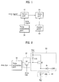
- Fig. 1 is a block diagram showing an apparatus for controlling a gray panel for a display panel according to the present invention.
- the apparatus for controlling a gray level for a display panel driven according to the present invention includes a pulse modulation part 30 for pulse amplitude modulating some of bits of externally input data corresponding to the gray level for the display panel and pulse width modulating the other bits to apply them to data lines, a switch part 10 for switching the pulse modulated data of the data lines in accordance with scan line signals, and a drive part 20 for controlling the gray level for the display panel corresponding to the data applied from the switch part 10.
- the drive part 20 includes a charge storage capacitor Cch connected with a positive power source Vdd, and a driving transistor Q2 for applying charges accumulated in the capacitor as much as a difference value between the data line signal and the positive power source Vdd to the display panel so as to drive the display panel.
- the switch part 10 includes a switching transistor Q3 for switching the data line signals using the scan line signals.
- the positive power source Vdd is connected with a driving transistor Q2 and the charge storage capacitor Cch is connected between the positive power source Vdd and the driving transistor Q2.
- the driving transistor Q3 is connected with the driving transistor Q2 and the pulse modulation part 30.
- a diode D1 for protecting a voltage is additionally provided.
- the diode D1 is connected in parallel between the driving transistor Q2 and the display panel to prevent error operation and voltage breakdown of the driving transistor Q2 resulting from voltage drop of the driving transistor Q2.
- the pulse modulation part 30 includes a control part 33 for dividing the input data into bits of first and second groups, a pulse amplitude modulation part 32 for pulse amplitude modulating the bits of the first group among the bits divided by the control part 33, and a pulse width modulation part 31 for pulse width modulating the bits of the second group among the bits divided by the control part 33.
- control part 33 divides the input data value into the bits of the first and second groups.
- the input data value is divided into two groups depending on conditions of the panel or design conditions of the driving circuit.
- the input data value is 8 bits, it is divided into four high bits and four low bits, or arbitrary bits are selected to be divided into two groups.
- the bits of the first group among the divided bits are pulse amplitude modulated and then the bits of the second group are pulse width modulated.
- the bits of the first group are pulse width modulated and then the bits of the second group are pulse amplitude modulated.
- CQ1 to CQN of the pulse amplitude modulation part 32 shown in Fig. 4 are generated as much as the number of bits used to control the amount of total current, and pulse amplitude modulate the bits selected by the control part.
- the data pulse modulated by the pulse modulation part 30 are applied to the data lines, a voltage corresponding to the data is input to the charge storage capacitor Cch and the driving transistor Q2 through the switching transistor Q3.
- the gray level for the display panel is controlled in accordance with the pulse modulated data input through the capacitor Cch and the driving transistor Q2.
- the switching transistor Q3 is controlled by the scan lines.
- each pixel the gray level is controlled under the control of the data and scan lines, and each pixel having the controlled gray level displays one image.
- the scan lines have a sinusoidal waveform equal to the pulse width modulated and applied to the data line.
- the gray level for the display panel has a great width. This facilitates control of the gray level and thus can finely control the gray level.
- Fig. 5 is a timing chart showing a driving waveform for a display panel according to the present invention.
- the data signal has been divided into four low bits and four high bits, the data signal may be divided into even bits and odd bits.
- the data signal may variously be divided depending on designs.
- the data signal is divided into four levels as follows.
- Fig. 5 shows how respective waveforms are varied.
- the four low bits show current level while the four high bits show pulses having different pulses at Te, Td, Tc, and Tb in sequence.
- the gray level for the display panel shows 256 levels based on data of 8 bits. Since the minimum level that can be identified by a human body is about 300pA, the minimum current level is defined as about 300pA. The maximum current level for the maximum gray level is defined as about 100nA.
- the current range becomes great, thereby facilitating control of the gray levels. That is, one frame time is divided at a proper ratio using four high bits among data of 8 bits. The intensity of the current is controlled using four low bits that show a current level.
- the current level is 50nA when the data is "0001" while the current level is 100nA when the data is "1111".
- the minimum gray level for the display panel requires the current of about 300pA when the data of 8 bits is used
- the minimum gray level for the display panel requires the current of about 50nA
- the maximum gray level requires the current of about 100nA when the data of 4 bits is used.
- the current range is about 389pA when the data is 8 bits while the current range is five times equivalent to about 3nA when the data is 4 bits. Therefore, it is easy to control the current and a problem related to leakage current can be solved.
- the current range of four low bits that show a current level is 1 ⁇ A
- the intensity of the minimum current is 1 ⁇ A
- the intensity of the maximum current is 15 ⁇ m.
- the range of the pulse widths of the four high bits is defined as 1, 2, 4, 8 ⁇ s.
- the switching time of the switching transistor Q3 becomes longer if the data pulse width applied through the data line is great.
- Brightness of the display panel becomes high if applying time of the current to the display panel becomes long.
- brightness of the display panel can be controlled by controlling the size of the data pulse width even if the driving transistor Q2 or the storage capacitor Cch is used in the same manner as the related art.
- the pulse width from Ta to Te shown in Fig. 5 can be obtained as follows.
- the size of the current controlled by the data line is in close relation with the pulse size.
- the intensity of the current and brightness according to the respective time can be obtained by the process for fabricating the display panel.
- the size of each time should be satisfied with the following conditions. 0 ⁇ s ⁇ Ta ⁇ Tb ⁇ Tc ⁇ Td ⁇ Te ⁇ T frame
- the respective time is divided into four levels but can be divided into various levels depending on design conditions of a driving integrated circuit.
- the gray level for the display panel can easily be controlled by the pulse modulation part 30 while the related art active driving circuit is used.
- the described apparatus and method for controlling a gray level for a display panel has the following advantages.
- the related art active driving circuit that can easily be designed is used and the data applied to the display panel is divided. Some of the data is pulse amplitude modulated to easily control the gray level for the display panel and the other data is pulse width modulated to easily control brightness of the display panel. Also, even if the leakage current is generated, no load of the capacitor size exists, thereby enabling free design.
Landscapes
- Physics & Mathematics (AREA)
- Engineering & Computer Science (AREA)
- General Physics & Mathematics (AREA)
- Computer Hardware Design (AREA)
- Theoretical Computer Science (AREA)
- Nonlinear Science (AREA)
- Chemical & Material Sciences (AREA)
- Crystallography & Structural Chemistry (AREA)
- Mathematical Physics (AREA)
- Optics & Photonics (AREA)
- Control Of Indicators Other Than Cathode Ray Tubes (AREA)
- Electroluminescent Light Sources (AREA)
- Liquid Crystal Display Device Control (AREA)
Abstract
Description
Claims (7)
- A method for controlling a gray level for a display panel driven by a plurality of scan line signals and a plurality of data line signals characterized in that some bits of the respective data are pulse amplitude modulated and the other bits are pulse width modulated (PWM) so as to control the gray level for the display panel.
- A method for controlling a gray level for a display panel driven by a plurality of scan line signals and a plurality of data line signals comprising the steps of:a) externally inputting a data value corresponding to the gray level for the display panel;b) dividing the input data value into bits of first and second groups;c) either pulse width modulating the bits of the second group after pulse amplitude modulating the bits of the first group or pulse amplitude modulating the bits of the second group after pulse width modulating the bits of the first group; andd) inputting the modulated data value to a corresponding data line to control the gray level for the display panel.
- An apparatus for controlling a gray level for a display panel driven by a plurality of scan line signals and a plurality of data line signals comprising:a pulse modulation part for pulse amplitude modulating some of bits of externally input data corresponding to the gray level for the display panel and pulse width modulating the other bits to apply them to the data lines;a switch part for switching the pulse modulated data of the data lines in accordance with the scan line signals; anda drive part for controlling the gray level for the display panel corresponding to the data applied from the switch part to drive the display panel.
- The apparatus of claim 3, wherein the pulse modulation part includes:a control part for dividing the input data into bits of first and second groups;a pulse amplitude modulation part for pulse amplitude modulating the bits of the first group among the bits divided by the control part; anda pulse width modulation part for pulse width modulating the bits of the second group among the bits divided by the control part.
- The apparatus of claim 3, wherein the drive part includes:a power source part;a charge storage capacitor connected with the power source part and the switch part, for storing a voltage corresponding to the difference between a voltage applied from the power source part and a voltage applied from the switch part; anda driver connected with the power source part and the capacitor, for driving the display panel in accordance with the voltage of the capacitor.
- The apparatus of claim 5, further comprising a diode connected in parallel between the driver and a driving pixel of the display panel.
- A display panel comprising the apparatus of any of claims 3 to 6.
Applications Claiming Priority (2)
| Application Number | Priority Date | Filing Date | Title |
|---|---|---|---|
| KR1020000011057A KR100327375B1 (en) | 2000-03-06 | 2000-03-06 | apparatus for active driver |
| KR2000011057 | 2000-03-06 |
Publications (3)
| Publication Number | Publication Date |
|---|---|
| EP1132883A2 true EP1132883A2 (en) | 2001-09-12 |
| EP1132883A3 EP1132883A3 (en) | 2002-10-02 |
| EP1132883B1 EP1132883B1 (en) | 2006-07-26 |
Family
ID=36848386
Family Applications (1)
| Application Number | Title | Priority Date | Filing Date |
|---|---|---|---|
| EP01302039A Expired - Lifetime EP1132883B1 (en) | 2000-03-06 | 2001-03-06 | Apparatus and method for controlling gray level for display panel |
Country Status (5)
| Country | Link |
|---|---|
| US (1) | US7119773B2 (en) |
| EP (1) | EP1132883B1 (en) |
| KR (1) | KR100327375B1 (en) |
| CN (1) | CN1151662C (en) |
| DE (1) | DE60121650T2 (en) |
Cited By (4)
| Publication number | Priority date | Publication date | Assignee | Title |
|---|---|---|---|---|
| WO2003094137A3 (en) * | 2002-05-02 | 2004-01-08 | Philips Intellectual Property | Improved driver for non-linear displays comprising a random access memory for static content |
| WO2009064352A1 (en) * | 2007-11-09 | 2009-05-22 | Eastman Kodak Company | Display device |
| WO2013045869A1 (en) * | 2011-09-28 | 2013-04-04 | Cambridge Display Technology Limited | Oled display device having some of the pixels containing two diodes with organic layers of different thickness |
| US9450036B2 (en) | 2002-01-24 | 2016-09-20 | Semiconductor Energy Laboratory Co., Ltd. | Semiconductor device and method of driving the semiconductor device |
Families Citing this family (28)
| Publication number | Priority date | Publication date | Assignee | Title |
|---|---|---|---|---|
| US6956547B2 (en) * | 2001-06-30 | 2005-10-18 | Lg.Philips Lcd Co., Ltd. | Driving circuit and method of driving an organic electroluminescence device |
| US7227517B2 (en) * | 2001-08-23 | 2007-06-05 | Seiko Epson Corporation | Electronic device driving method, electronic device, semiconductor integrated circuit, and electronic apparatus |
| JP2006523328A (en) * | 2003-04-04 | 2006-10-12 | コーニンクレッカ フィリップス エレクトロニクス エヌ ヴィ | Display device |
| US7663589B2 (en) * | 2004-02-03 | 2010-02-16 | Lg Electronics Inc. | Electro-luminescence display device and driving method thereof |
| KR100997477B1 (en) * | 2004-04-29 | 2010-11-30 | 삼성에스디아이 주식회사 | Field emission display device with variable gradation expression |
| US20060139265A1 (en) * | 2004-12-28 | 2006-06-29 | Semiconductor Energy Laboratory Co., Ltd. | Driving method of display device |
| JP4483725B2 (en) * | 2005-07-04 | 2010-06-16 | セイコーエプソン株式会社 | LIGHT EMITTING DEVICE, ITS DRIVE CIRCUIT, AND ELECTRONIC DEVICE |
| CN100508010C (en) * | 2006-03-23 | 2009-07-01 | 矽创电子股份有限公司 | Driving method for increasing gray scale |
| CN101393726B (en) * | 2007-09-21 | 2011-02-02 | 北京京东方光电科技有限公司 | Pixel grey scale spreading method, pixel capacitor charging time driving method and device |
| KR101042956B1 (en) * | 2009-11-18 | 2011-06-20 | 삼성모바일디스플레이주식회사 | Pixel circuit and organic light emitting display device using the same |
| JP5733077B2 (en) * | 2011-07-26 | 2015-06-10 | セイコーエプソン株式会社 | ELECTRO-OPTICAL DEVICE, ELECTRO-OPTICAL DEVICE POWER SUPPLY METHOD, AND ELECTRONIC DEVICE |
| CN102332247A (en) * | 2011-11-25 | 2012-01-25 | 深圳市摩西尔电子有限公司 | Method for adjusting LED (Light Emitting Diode) gray scale |
| US11100840B2 (en) * | 2019-03-29 | 2021-08-24 | Samsung Electronics Co., Ltd. | Display panel and driving method of the display panel |
| TWI714071B (en) * | 2019-05-01 | 2020-12-21 | 友達光電股份有限公司 | Pixel circuit and display device |
| EP3754639B1 (en) * | 2019-06-17 | 2023-09-27 | Samsung Electronics Co., Ltd. | Display module and driving method thereof |
| US11138934B2 (en) * | 2019-07-30 | 2021-10-05 | Innolux Corporation | Display device |
| TWI706400B (en) * | 2019-08-13 | 2020-10-01 | 友達光電股份有限公司 | Pixel circuit and driving method for the same |
| CN110570821A (en) * | 2019-09-18 | 2019-12-13 | 广东晟合技术有限公司 | OLED optical compensation method, compensation device and display driving chip |
| TWI716160B (en) * | 2019-10-22 | 2021-01-11 | 友達光電股份有限公司 | Pixel circuit |
| CN111462685B (en) * | 2020-05-29 | 2021-08-31 | 上海天马有机发光显示技术有限公司 | A pixel driving circuit and driving method thereof, display panel and display device |
| CN115699152B (en) | 2020-10-08 | 2025-01-10 | 三星电子株式会社 | Electronic device and control method thereof |
| TWI781756B (en) * | 2021-03-02 | 2022-10-21 | 友達光電股份有限公司 | Driving circuit and driving method |
| US11663960B2 (en) * | 2021-08-19 | 2023-05-30 | Innolux Corporation | Electronic device |
| US11810512B2 (en) * | 2021-12-16 | 2023-11-07 | Tcl China Star Optoelectronics Technology Co., Ltd. | Pixel circuit and display panel |
| KR102694048B1 (en) * | 2022-01-17 | 2024-08-09 | 한국전자통신연구원 | Pixel circuit driving method and pixel circuit therefor and display module using the same |
| KR102750508B1 (en) * | 2022-12-20 | 2025-01-07 | 주식회사 사피엔반도체 | Display device combining driving methods |
| KR102534473B1 (en) * | 2023-01-27 | 2023-05-30 | 주식회사 티엘아이 | Display device with high resolution of display image and low current consumption |
| KR20250132226A (en) * | 2024-02-28 | 2025-09-04 | 엘지디스플레이 주식회사 | Timing controller |
Family Cites Families (21)
| Publication number | Priority date | Publication date | Assignee | Title |
|---|---|---|---|---|
| KR900000643B1 (en) * | 1959-03-26 | 1990-02-02 | 산요덴끼 가부시기가이샤 | Inverter apparatus |
| GB1362185A (en) * | 1970-07-07 | 1974-07-30 | Avery Denison Ltd | Dynamic balancing machines |
| JPS6010629B2 (en) * | 1977-06-20 | 1985-03-19 | シャープ株式会社 | Driving method of thin film EL element |
| US4366504A (en) * | 1977-10-07 | 1982-12-28 | Sharp Kabushiki Kaisha | Thin-film EL image display panel |
| US4199697A (en) * | 1978-07-05 | 1980-04-22 | Northern Telecom Limited | Pulse amplitude modulation sampling gate including filtering |
| US4338598A (en) * | 1980-01-07 | 1982-07-06 | Sharp Kabushiki Kaisha | Thin-film EL image display panel with power saving features |
| EP0261896B1 (en) * | 1986-09-20 | 1993-05-12 | THORN EMI plc | Display device |
| US5061880A (en) * | 1989-03-22 | 1991-10-29 | Matsushita Electric Industrial Co., Ltd. | Method of driving image display device |
| US5701134A (en) * | 1990-05-24 | 1997-12-23 | U.S. Philips Corporation | Picture display device with uniformity correction of electron supply |
| US5280280A (en) * | 1991-05-24 | 1994-01-18 | Robert Hotto | DC integrating display driver employing pixel status memories |
| US5671003A (en) * | 1991-11-04 | 1997-09-23 | Eastman Kodak Company | Hybrid digital image printer with halftone gray scale capability |
| US5652600A (en) * | 1994-11-17 | 1997-07-29 | Planar Systems, Inc. | Time multiplexed gray scale approach |
| US5757348A (en) * | 1994-12-22 | 1998-05-26 | Displaytech, Inc. | Active matrix liquid crystal image generator with hybrid writing scheme |
| US6529178B1 (en) | 1997-02-17 | 2003-03-04 | Seiko Epson Corporation | Current-driven emissive display device, method for driving the same, and method for manufacturing the same |
| US6023259A (en) * | 1997-07-11 | 2000-02-08 | Fed Corporation | OLED active matrix using a single transistor current mode pixel design |
| JPH1152917A (en) * | 1997-07-30 | 1999-02-26 | Sanyo Electric Co Ltd | Liquid crystal driving method |
| US5969579A (en) * | 1997-10-17 | 1999-10-19 | Ncr Corporation | ECL pulse amplitude modulated encoder driver circuit |
| GB9803441D0 (en) | 1998-02-18 | 1998-04-15 | Cambridge Display Tech Ltd | Electroluminescent devices |
| CN1287652A (en) | 1998-09-08 | 2001-03-14 | Tdk株式会社 | Device for organic EL display and driving method |
| JP3353731B2 (en) * | 1999-02-16 | 2002-12-03 | 日本電気株式会社 | Organic electroluminescence element driving device |
| US6618031B1 (en) | 1999-02-26 | 2003-09-09 | Three-Five Systems, Inc. | Method and apparatus for independent control of brightness and color balance in display and illumination systems |
-
2000
- 2000-03-06 KR KR1020000011057A patent/KR100327375B1/en not_active Expired - Lifetime
-
2001
- 2001-03-02 US US09/798,718 patent/US7119773B2/en not_active Expired - Lifetime
- 2001-03-06 CN CNB011092904A patent/CN1151662C/en not_active Expired - Lifetime
- 2001-03-06 EP EP01302039A patent/EP1132883B1/en not_active Expired - Lifetime
- 2001-03-06 DE DE60121650T patent/DE60121650T2/en not_active Expired - Lifetime
Cited By (8)
| Publication number | Priority date | Publication date | Assignee | Title |
|---|---|---|---|---|
| US9450036B2 (en) | 2002-01-24 | 2016-09-20 | Semiconductor Energy Laboratory Co., Ltd. | Semiconductor device and method of driving the semiconductor device |
| US10355068B2 (en) | 2002-01-24 | 2019-07-16 | Semiconductor Energy Laboratory Co., Ltd. | Semiconductor device and method of driving the semiconductor device |
| US11121203B2 (en) | 2002-01-24 | 2021-09-14 | Semiconductor Energy Laboratory Co., Ltd. | Semiconductor device and method of driving the semiconductor device |
| WO2003094137A3 (en) * | 2002-05-02 | 2004-01-08 | Philips Intellectual Property | Improved driver for non-linear displays comprising a random access memory for static content |
| CN1650341B (en) * | 2002-05-02 | 2012-04-25 | 三叉微系统(远东)有限公司 | Improved driver for non-linear displays comprising a random access memory for static content |
| WO2009064352A1 (en) * | 2007-11-09 | 2009-05-22 | Eastman Kodak Company | Display device |
| WO2013045869A1 (en) * | 2011-09-28 | 2013-04-04 | Cambridge Display Technology Limited | Oled display device having some of the pixels containing two diodes with organic layers of different thickness |
| GB2509270A (en) * | 2011-09-28 | 2014-06-25 | Cambridge Display Tech Ltd | Oled display device having some of the pixels containing two diodes with organic layers of different thickness |
Also Published As
| Publication number | Publication date |
|---|---|
| CN1151662C (en) | 2004-05-26 |
| EP1132883B1 (en) | 2006-07-26 |
| EP1132883A3 (en) | 2002-10-02 |
| KR100327375B1 (en) | 2002-03-06 |
| KR20010087003A (en) | 2001-09-15 |
| DE60121650T2 (en) | 2007-07-12 |
| DE60121650D1 (en) | 2006-09-07 |
| US20010019319A1 (en) | 2001-09-06 |
| CN1321043A (en) | 2001-11-07 |
| US7119773B2 (en) | 2006-10-10 |
Similar Documents
| Publication | Publication Date | Title |
|---|---|---|
| EP1132883A2 (en) | Apparatus and method for controlling gray level for display panel | |
| US8125473B2 (en) | Electro-luminescence display device | |
| US7460101B2 (en) | Frame buffer pixel circuit for liquid crystal display | |
| US6215466B1 (en) | Method of driving an electro-optical device | |
| US5973456A (en) | Electroluminescent display device having uniform display element column luminosity | |
| KR100517153B1 (en) | Image display device and image display method, and recording medium for recording image display program | |
| US6566643B2 (en) | Electro-optical device, method of driving the same, and electronic apparatus using the same | |
| US7463224B2 (en) | Light emitting device and display device | |
| KR101652015B1 (en) | Liquid crystal display device and method of driving the same | |
| KR102655248B1 (en) | Display device | |
| KR102661084B1 (en) | Electronic Device Capable of Reducing Color Shift | |
| US7126592B2 (en) | Forming modulated signals that digitally drive display elements | |
| KR101070125B1 (en) | Display device and control method thereof | |
| US20050052401A1 (en) | Display apparatus, device for driving the display apparatus, and method of driving the display apparatus | |
| US20080043007A1 (en) | Active Matrix Array Device and Method for Driving Such Device | |
| CN117079600A (en) | Pixel circuit and driving method thereof and display panel | |
| KR20030057965A (en) | Method and apparatus of driving electro luminescence panel | |
| KR100421873B1 (en) | Analog driving circuit in display element | |
| JPH10111667A (en) | Capacitive load driving circuit and plasma display using the same | |
| US6590556B2 (en) | Active matrix display device | |
| US20080062073A1 (en) | Image Display Device and Method of Controlling Same | |
| US7245296B2 (en) | Active matrix display device | |
| EP1602100A2 (en) | Active matrix array device, electronic device having an active matrix array device and picture quality improvement method for such an electronic device | |
| KR100453186B1 (en) | Ferroelectric liquid crystal display device and its driving method | |
| KR100848954B1 (en) | Driving device and method of electroluminescent panel |
Legal Events
| Date | Code | Title | Description |
|---|---|---|---|
| PUAI | Public reference made under article 153(3) epc to a published international application that has entered the european phase |
Free format text: ORIGINAL CODE: 0009012 |
|
| AK | Designated contracting states |
Kind code of ref document: A2 Designated state(s): AT BE CH CY DE DK ES FI FR GB GR IE IT LI LU MC NL PT SE TR |
|
| AX | Request for extension of the european patent |
Free format text: AL;LT;LV;MK;RO;SI |
|
| PUAL | Search report despatched |
Free format text: ORIGINAL CODE: 0009013 |
|
| AK | Designated contracting states |
Kind code of ref document: A3 Designated state(s): AT BE CH CY DE DK ES FI FR GB GR IE IT LI LU MC NL PT SE TR |
|
| AX | Request for extension of the european patent |
Free format text: AL;LT;LV;MK;RO;SI |
|
| 17P | Request for examination filed |
Effective date: 20030204 |
|
| 17Q | First examination report despatched |
Effective date: 20030415 |
|
| AKX | Designation fees paid |
Designated state(s): DE FR GB |
|
| GRAP | Despatch of communication of intention to grant a patent |
Free format text: ORIGINAL CODE: EPIDOSNIGR1 |
|
| GRAS | Grant fee paid |
Free format text: ORIGINAL CODE: EPIDOSNIGR3 |
|
| GRAA | (expected) grant |
Free format text: ORIGINAL CODE: 0009210 |
|
| AK | Designated contracting states |
Kind code of ref document: B1 Designated state(s): DE FR GB |
|
| REG | Reference to a national code |
Ref country code: GB Ref legal event code: FG4D |
|
| REF | Corresponds to: |
Ref document number: 60121650 Country of ref document: DE Date of ref document: 20060907 Kind code of ref document: P |
|
| ET | Fr: translation filed | ||
| PLBE | No opposition filed within time limit |
Free format text: ORIGINAL CODE: 0009261 |
|
| STAA | Information on the status of an ep patent application or granted ep patent |
Free format text: STATUS: NO OPPOSITION FILED WITHIN TIME LIMIT |
|
| 26N | No opposition filed |
Effective date: 20070427 |
|
| GBPC | Gb: european patent ceased through non-payment of renewal fee |
Effective date: 20070306 |
|
| PG25 | Lapsed in a contracting state [announced via postgrant information from national office to epo] |
Ref country code: GB Free format text: LAPSE BECAUSE OF NON-PAYMENT OF DUE FEES Effective date: 20070306 |
|
| REG | Reference to a national code |
Ref country code: GB Ref legal event code: 732E |
|
| REG | Reference to a national code |
Ref country code: FR Ref legal event code: TP |
|
| REG | Reference to a national code |
Ref country code: FR Ref legal event code: PLFP Year of fee payment: 16 |
|
| REG | Reference to a national code |
Ref country code: FR Ref legal event code: PLFP Year of fee payment: 17 |
|
| REG | Reference to a national code |
Ref country code: FR Ref legal event code: PLFP Year of fee payment: 18 |
|
| PGFP | Annual fee paid to national office [announced via postgrant information from national office to epo] |
Ref country code: DE Payment date: 20200121 Year of fee payment: 20 |
|
| PGFP | Annual fee paid to national office [announced via postgrant information from national office to epo] |
Ref country code: FR Payment date: 20200123 Year of fee payment: 20 |
|
| REG | Reference to a national code |
Ref country code: DE Ref legal event code: R071 Ref document number: 60121650 Country of ref document: DE |