EP1132815A2 - Cross-bar switch system with redundancy - Google Patents
Cross-bar switch system with redundancy Download PDFInfo
- Publication number
- EP1132815A2 EP1132815A2 EP01105387A EP01105387A EP1132815A2 EP 1132815 A2 EP1132815 A2 EP 1132815A2 EP 01105387 A EP01105387 A EP 01105387A EP 01105387 A EP01105387 A EP 01105387A EP 1132815 A2 EP1132815 A2 EP 1132815A2
- Authority
- EP
- European Patent Office
- Prior art keywords
- cross
- bar
- bar switch
- nodes
- outputs
- Prior art date
- Legal status (The legal status is an assumption and is not a legal conclusion. Google has not performed a legal analysis and makes no representation as to the accuracy of the status listed.)
- Withdrawn
Links
Images

Classifications
-
- H—ELECTRICITY
- H04—ELECTRIC COMMUNICATION TECHNIQUE
- H04L—TRANSMISSION OF DIGITAL INFORMATION, e.g. TELEGRAPHIC COMMUNICATION
- H04L49/00—Packet switching elements
- H04L49/55—Prevention, detection or correction of errors
- H04L49/552—Prevention, detection or correction of errors by ensuring the integrity of packets received through redundant connections
-
- H—ELECTRICITY
- H04—ELECTRIC COMMUNICATION TECHNIQUE
- H04L—TRANSMISSION OF DIGITAL INFORMATION, e.g. TELEGRAPHIC COMMUNICATION
- H04L49/00—Packet switching elements
- H04L49/10—Packet switching elements characterised by the switching fabric construction
- H04L49/101—Packet switching elements characterised by the switching fabric construction using crossbar or matrix
Definitions
- This invention relates to a computer system and, more particularly, to a system in which crossbar switches for connecting CPUs and memory of a computer or for connecting the nodes in a computer system constituted by multiple nodes are provided with redundancy.
- crossbar switches are used to switchingly connect the CPUs and memory of a computer, for example, or the nodes in a computer system constituted by multiple nodes.
- Crossbar switches are constructed on a plurality of LSI chips or cards or on a single LSI chip, which includes a plurality of crossbar switch blocks, in accordance with the bit slice or byte slice, etc.
- N ⁇ N crossbar switch device is provided with an (N+1) th standby input line to construct an (N+1) ⁇ N cross-bar switch device. If an abnormality is detected in one of the N-number of working lines, a changeover is made to the standby line by a spatial switch, thereby furnishing data with an alternative path.
- JP-A-11-331374 discloses a device serving as a cross-bar switch device used in an ATM switch or the like, wherein problems associated with the redundant cross-bar switch device (i.e., the fact that the switch is left in operation with no measures being taken to restore a faulty location) described in the aforesaid specification of JP-A-7-264198 are intended to be solved.
- a crossbar switch unit which accommodates N-number of ports and implements a function for switching between any two of these ports, comprises a plurality of N ⁇ N cross-bar switch cards.
- the device further includes N-number of ports connected to the cross-bar switch unit by a plurality of working lines and at least one standby line, and a connection controller for outputting a switch-abnormality detection signal upon detecting a switch abnormality in the cross-bar switch unit set in response to a switch signal.
- a port responds to the switch-abnormality detection signal by changing over at least one working line to at least one standby line.
- an object of the present invention is to provide a crossbar switch system in which rapid recovery of the system can be achieved at low cost when a crossbar switch fails.
- a crossbar switch system comprising N+1 crossbar switches of which N is required and one is redundant.
- a failure processing circuit recognizes that a crossbar switch is faulty and controls selection circuits, which are provided at input/outputs of the crossbar switches, after the system is restarted. As a result, the faulty crossbar switch is taken out of service and the redundant crossbar switch is placed in service.
- a cross-bar switch system with redundancy having a cross-bar switch set of a redundant structure comprising a plurality of cross-bar switches necessary for effecting connections between nodes of a plurality of nodes, and at least one additional redundant cross-bar switch;
- a cross-bar switch system having N+1 cross-bar switches inclusive of redundancy wherein one cross-bar switch is provided in addition to N cross-bar switches required for connecting of nodes among first to Mth nodes (where M is a prescribed integer equal to or greater than 2) ; the first cross-bar switch receiving each first output among N outputs of each of the first to Mth nodes at M input terminals thereof; the (N+1) th cross-bar switch receiving each Nth output among N outputs of each of the first to Nth nodes at M input terminals thereof; an Ith (where I is an integer of 2 or more and not more than N) cross-bar switch having M selection circuits, which are provided at respective ones of M input terminal thereof, to each of which are input consecutive (I-1)th and Ith outputs, which correspond to the Ith cross-bar switch, among outputs of each of the first to Mth nodes; and a Jth (where J is an integer of 1 or more and not more than M)
- the crossbar switches connect CPUs and a memory within a computer or perform switching between nodes of a multinode system having CPUs and memories wherein the memories of remote nodes are accessed via the crossbar switches.
- a cross-bar switch system with redundancy in a system having cross-bar switches for connecting CPUs and a memory within a computer system or for connecting nodes in a computer system composed of a plurality of nodes, a cross-bar switch system with redundancy according to a fifth aspect comprises;
- Each of said nodes inputs and outputs N bytes of data preferably on a byte-by-byte basis.
- the failure-processing circuit includes: an (N+1) -bit cross-bar switch failure information register for storing whether failure has occurred or not with regard to the first to (N+1)th cross-bar switches; a selection-circuit control output circuit for outputting a selection control signal to each of the selection circuits based upon values in the cross-bar switch failure information register; and a multiple-failure detector for informing a system controller of occurrence of multiple failure when multiple cross-bar switches fail.
- M and N may be equal values.
- the system is provided with N+1 crossbar switches of which N are required and one is redundant. If a failure processing circuit recognizes failure of a cross-bar switch when such a failure occurs in the system, the failure processing circuit controls selection circuits, which are provided at inputs and outputs of the cross-bar switches, after the system is restarted, to thereby take the faulty cross-bar switch out of service and place the redundant cross-bar switch in service.
- an Ith (where I is an integer equal to or greater than 2 and not more than N) cross-bar switch (cross-bar switches 11 to 17 in Fig. 1) has first to Mth selection circuits (11-0 to 11-7, ⁇ , 17-0 to 17-7), which are provided at the input thereof, to each of which are input two signals, namely an (I-1)th output signal and an Ith output signal, of each of the first to Mth nodes;
- a Jth (where J is an integer equal to or greater than 1 and not more than M) node has M selection circuits (0-0 to 0-7, 1-0 to 1-7, ⁇ , 7-0 to 7-7), which are provided at N input terminals thereof, to each of which are input outputs of a Jth output port of each of mutually adjacent cross-bar switches among the first to (N+1) th cross-bar switches, namely of Kth and (K+1) th (where K is an integer equal to or greater than 1 and not
- each node inputs and outputs first to Nth items of data on a byte-by-byte basis.
- the failure processing circuit has an (N+1)-bit cross-bar switch failure information register (200) for storing failure information, which is output from a system controller, regarding the N+1 cross-bar switches; a selection-circuit control output circuit (201) for outputting a selection control signal to the selection circuits; and a multiple-failure detector (202) for informing the system controller of occurrence of multiple failure when multiple cross-bar switches fail.
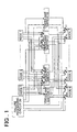
- Fig. 1 is a diagram illustrating the configuration of a crossbar switch system according to an embodiment of the present invention. As shown in Fig. 1, the system includes eight nodes 0 to 7, nine cross-bar switches 10 to 18, a failure processing circuit 20, and selection circuits 0-0 to 0-7, ⁇ , 7-0 to 7-7, 11-0 to 11-7, ⁇ , and 17-0 to 17-7.
- the nodes 0 to 7 are identically constructed and so are the crossbar switches 10 to 18.
- Each of the cross-bar switches 10 to 18 has eight input ports, eight output ports, an 8 ⁇ 8 cross-bar switch unit (not shown) and a connection controller (not shown) for controlling switching of the input and output ports to the cross-bar switch unit.
- Each port is constructed to input or output data on a per-byte (8-bit) basis.
- Fig. 1 is mainly for the purpose of describing the principle of the present invention; the number of nodes, for example, is not limited to eight, as a matter of course.
- the cross-bar switches and the failure detection reference is made to JP-A-11-331374 which is incorporated herein by reference thereto.
- Data communicated between any two nodes of the nodes 0 to 7 is transferred from the source node to the destination node by the crossbar switches 10 to 18.
- Byte-0 data of the 8-byte data output from respective ones of the nodes 0 to 7 is input to the crossbar switch 10 at a respective one of the eight input ports.
- cross-bar switch 11 With regard to cross-bar switch 11, byte-0 data and byte-1 data output from node 0 is input to the selection switch 11-0, the output of the selection switch 11-0 is applied to the first input port of the cross-bar switch 11, byte-0 data and byte-1 data output from node 1 is input to the selection switch 11-1, and the output of the selection switch 11-1 is applied to the second input port of the cross-bar switch 11. Similarly, byte-0 data and byte-1 data output from node 7 is input to the selection switch 11-7 and the output of the selection switch 11-7 is applied to the eighth input port of the cross-bar switch 11.
- the selection circuits 11-0 to 11-7 select one of byte-0 data and byte-1 data in the 8-byte data output from the nodes 0 to 7 and output the selected data to the cross-bar switch 11.
- the selection circuits 11-0 to 11-7 select the byte-1 data in the absence of a failure and select the byte-0 data when the crossbar switch 10 fails (see Fig. 4, described later).
- cross-bar switch 17 With regard to cross-bar switch 17, byte-6 data and byte-7 data output from node 0 is input to the selection switch 17-0, the output of the selection switch 17-0 is applied to the first input port of the cross-bar switch 17, byte-6 data and byte7 data output from node 1 is input to the selection switch 17-1, and the output of the selection switch 17-1 is applied to the second input port of the cross-bar switch 17. Similarly, byte-6 data and byte-7 data output from node 7 is input to the selection switch 17-7 and the output of the selection switch 17-7 is applied to the eighth input port of the cross-bar switch 17.
- the byte-7 data in the 8-byte data output from each of the nodes 0 to 7 enters respective ones of the eight input ports of crossbar switch 18.
- the data output from the cross-bar switches 10 to 18 is selected by the selection circuits 0-0 to 0-7, 1-0 to 1-7, ⁇ , 7-0 to 7-7 and input to the nodes 0 to 7.
- the selection circuit 0-0 corresponding to node 0 receives as inputs the byte-0 data output from the first output port of cross-bar switch 10 and the byte-0 data output from the first output port of cross-bar switch 11, selects one of these inputs based upon the control signal from the failure processing circuit 20 and outputs the selected data to the node 0.
- the selection circuit 0-7 corresponding to node 0 receives as inputs the byte-7 data output from the first output port of cross-bar switch 17 and the byte-7 data output from the first output port of cross-bar switch 18, selects one of these inputs based upon the control signal from the failure processing circuit 20 and outputs the selected data to the node 0.
- the selection circuit 7-0 corresponding to node 7 receives as inputs the byte-0 data output from the eighth output port of cross-bar switch 10 and the byte-0 data output from the eighth output port of cross-bar switch 11, selects one of these inputs based upon the control signal from the failure processing circuit 20 and outputs the selected data to the node 7.
- the selection circuit 7-7 selects byte-7 data, which is output from the eighth output port of cross-bar switch 17 and the eighth output port of cross-bar switch 18, based upon the control signal from the failure processing circuit 20 and outputs the selected data to the node 7.
- the failure processing circuit 20 On the basis of failure information relating to a failure that has occurred, the failure processing circuit 20 outputs the selection control signal to the selection circuits 0-0 to 0-7, 1-0 to 1-7, ⁇ , 7-0 to 7-7, 11-0 to 11-7, ⁇ , 17-0 to 17-7.
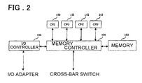
- Fig. 2 illustrates an example of the internal structure of the node 0 to 7 show in Fig. 1.
- Each node is composed of four CPUs 100 to 103, a memory controller 104, a memory 105 and an input/output (I/O) controller 106.
- I/O input/output
- Each of the CPUs 100 to 103 performs memory access and I/0 access via the memory controller 104.
- the memory 105 In a case where a CPU accesses the memory 105 within its own node, the memory 105 is accessed from the memory controller 104. However, when a memory within another node is accessed, the access request is sent from the memory controller 104 to a memory controller of the other node via a cross-bar switch, thereby accessing the memory within the other node.
- Fig. 3 illustrates the internal structure of the failure processing circuit 20 shown in Fig. 1.
- the failure processing circuit 20 outputs the selection control signal to the selection circuits 0-0 to 7-7, 11-0 to 17-7 after the system is restarted, for example, whereby control is performed in such a manner that the faulty crossbar switch is taken out of service and the redundant crossbar switch is placed in service.
- Failure information concerning the crossbar switches 10 to 18 output from a system controller enters a 9-bit crossbar switch failure information register 200.
- Each bit of the register 200 holds information as to whether the respective one of the cross-bar switches 10 to 18 is faulty or not.
- the information from the crossbar switch failure information register 200 is output to a selection-circuit control output circuit 201.
- the selection-circuit control output circuit 201 outputs a selection control signal to each of the selection circuits 0-0 to 7-7, 11-0 to 17-7.
- the information from the crossbar switch failure information register 200 is also output to a multiple-failure detector 202. If two or more of the crossbar switches 10 to 18 fail, the multiple-failure detector 202 notifies the system controller of the occurrence of multiple failure.
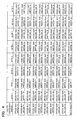
- Fig. 4 illustrates, in table form, which crossbar switches switch each byte of data transferred between nodes when the crossbar switches 10 to 18 fail.
- the crossbar switch 10 develops a failure
- the data of bytes 0 to 7 are switched by the crossbar switches 11 to 18, respectively, as indicated by the second row of the table of Fig. 4.
- any of the cross-bar switches 11 to 18 fails, then, in similar fashion, the data of each byte is switched by a respective one of the cross-bar switches indicated in Fig. 4 while the faulty cross-bar switch is avoided.
- the crossbar switches 10 to 18 are cross-bar switches in a redundant arrangement for effecting communication between nodes. If a failure has not occurred, the crossbar switches 10 to 17 are employed and the crossbar switch 18 is not used.
- the byte-0 data in the 8-byte data output from each of the nodes 0 to 7 is switched by the cross-bar switch 10, the byte-1 data is switched by the cross-bar switch 11 and the byte-7 data is switched by the cross-bar switch 17.
- the byte-0 data in 8-byte request data is switched by the cross-bar switch 10 and is sent to node 1.
- the selection circuit 11-0 responds to the control signal from the failure processing circuit 20 by selecting and outputting its other input, namely the byte-1 data in the 8-byte data from node 0.
- the byte-0 data output from the cross-bar switch 10 enters the selection circuit 1-0 which, in response to the selection control signal from the failure processing circuit 20, selects the byte-0 data and outputs this data to the node 1.
- the cross-bar switch 10 is taken out of service and the items of byte-0 data, byte-1 data and byte-7 data in the 8-byte data output from nodes 0 to 7 are switched by the cross-bar switches 11, 12 and 18, respectively.
- the byte-0 data that was output from node 0 to selection circuit 11-0 is selected by the selection control signal from the failure processing circuit 20 and is delivered to the cross-bar switch 11.
- the byte-0 data output from cross-bar switch 11 enters the selection circuit 1-0, and the latter responds to the selection control signal from the failure processing circuit 20 by selecting the byte-0 data and inputting it to the node 1.
- each byte of node transfer data is transferred by control similar to that set forth above via the cross-bar switches indicated in Fig. 4.
- the crossbar multiple-failure detector 202 in the failure processing circuit 20 detects multiple crossbar failure and so informs the system controller. In this case, the system is not restarted and remains down until it is repaired.
- each node outputs 8-byte data
- each selection circuit and each port of the crossbar switches inputs and outputs data in single-byte units.
- the present invention is not limited to this implementation and it goes without saying that an implementation in which data is input and output in word units or bit units may be adopted.
- the present invention is not only ideal for application to a multinode computer system but can be similarly applied to crossbar switches that control the connections between multiple CPUs and memories.
- the present invention has a number of advantageous effects, which will now be described.
- the failure processing circuit controls the selection circuits, which are provided at the inputs and outputs of each of the cross-bar switches, based upon failure information, thereby making it possible to achieve an operation in which the faulty cross-bar switch is avoided after the system is started up.
- cross-bar switch components in a case where a cross-bar switch is designed to be inserted into and withdrawn from a live wire, it is possible for cross-bar switch components to be replaced on-line. This means that maintenance can be performed without shutting down the system.
Landscapes
- Engineering & Computer Science (AREA)
- Computer Networks & Wireless Communication (AREA)
- Signal Processing (AREA)
- Computer Security & Cryptography (AREA)
- Physics & Mathematics (AREA)
- Mathematical Physics (AREA)
- Multi Processors (AREA)
- Use Of Switch Circuits For Exchanges And Methods Of Control Of Multiplex Exchanges (AREA)
- Data Exchanges In Wide-Area Networks (AREA)
- Hardware Redundancy (AREA)
Abstract
Description
M and N may be equal values.
Claims (8)
- A cross-bar switch system with redundancy having a cross-bar switch set of a redundant structure comprising a plurality of cross-bar switches necessary for effecting connections between nodes of a plurality of nodes, and at least one additional redundant cross-bar switch;(a) wherein a first cross-bar switch of said cross-bar switch set receives at input terminals thereof, first outputs among multiple N outputs of each of the plurality of nodes, and said one redundant cross-bar switch receives Nth outputs among N outputs of each of said plurality of nodes applied to input terminals thereof, N being in integer of 2 or more;(b) each of the remaining cross-bar switches has M selection circuits to each of which receives two consecutive outputs of an order corresponding to that of the cross-bar switch, among N outputs of each of said plurality of nodes, the outputs of these M selection circuits being input to the cross-bar switch provided that M is an integer of 2 or more;(c) each node of said plurality of nodes has N selection switches, which are provided at input terminals thereof, each of said selection switches receives two consecutive outputs of an output order corresponding to that of the node, among outputs of two mutually adjacent cross-bar switches, two by two, of said cross-bar switch set; and(d) in response to a selection control signal output from a failure processing circuit that executes cross-bar switch failure processing, each of said selection circuits selects and outputs one of its two inputs and, when one cross-bar switch fails, takes the failed cross-bar switch out of service.
- A cross-bar switch system with redundancy,(a) comprising N+1 cross-bar switches wherein one cross-bar switch is redundantly provided in addition to N cross-bar switches required for connecting of nodes among first to Mth nodes where M and N are prescribed integers equal to or greater than 2, respectively;(b) wherein the first cross-bar switch receives each first output among N outputs of each of said first to Mth nodes at M input terminals thereof;(c) the (N+1)th cross-bar switch receives each Nth output among N outputs of each of said first to Nth nodes at M input terminals thereof;(d) an Ith, where I is an integer of 2 or more and less than N, cross-bar switch having M selection circuits, which are provided at respective ones of M input terminals thereof, to each of which are input consecutive (I-1)th and Ith outputs, which correspond to said Ith cross-bar switch, among outputs of each of said first to Mth nodes; and(e) a Jth, where J is an integer of 1 or more and not more than M, node having N selection switches, which are provided at input terminals of said node, to each of which are input Jth outputs of two mutually adjacent cross-bar switches among said first to (N+1) th cross-bar switches, where N is an integer of 2 or more; and(f) wherein in response to a selection control signal output from a failure processing circuit that executes cross-bar switch failure processing, each of said selection circuits selects and outputs one of its two inputs and, when one cross-bar switch fails, takes the failed cross-bar switch out of service.
- A cross-bar switch system with redundancy,(a) comprising N+1 cross-bar switches wherein one cross-bar switch is redundantly provided in addition to N cross-bar switches required for connecting of nodes among first to Mth nodes, where M and N are prescribed integers of 2 or more, respectively;(b) each node of said first to Mth nodes outputting first to Mth output signals from output terminals thereof and receiving first to Nth input signals applied to input terminals thereof;(c) the first cross-bar switch receiving each first output signal of each of said first to Mth nodes at M input terminals thereof;(d) the (N+1)th cross-bar switch receiving each Nth output signal of each of said first to Mth nodes at M input terminals thereof;(e) an Ith, where I is an integer of 2 or more and not more than N cross-bar switch having M selection circuits, which are provided at respective ones of M input terminals thereof, to each of which are input two signals, namely an (I-1)th output signal and an Ith output signal, of each of said first to Mth nodes; and(f) a Jth, where J is an integer of 1 or more and not more than M, node having N selection circuits, which are provided at N input terminals thereof, to each of which are input outputs of a Jth output port of each of mutually adjacent cross-bar switches among said first to (N+1)th cross-bar switches, namely of Kth and (K+1)th cross-bar switches, where K is an integer of 1 or more and not more than N;(g) wherein in response to a selection control signal output from a failure processing circuit that executes cross-bar switch failure processing, each of said selection circuits selects and outputs one of two signals and, when one cross-bar switch fails, takes the failed cross-bar switch out of service.
- In a system having cross-bar switches for connecting CPUs and a memory within a computer system or for connecting nodes in a computer system composed of a plurality of nodes, a cross-bar switch system with redundancy comprising:(a) N+1 cross-bar switches inclusive of N cross-bar switches that are indispensable for the system and one redundant cross-bar switch;(b) selection circuits provided at inputs and outputs of said cross-bar switches; and(c) means, operable when the system fails, for performing control in such a manner that a cross-bar switch that has failed is taken out of service and the redundant cross-bar switch is placed in service by controlling said selection circuits by a failure processing circuit after the system is restarted, said failure processing circuit recognizing that said cross-bar switch has failed.
- The system according to claim 3, wherein each of said nodes inputs and outputs N bytes of data on a byte-by-byte basis.
- The system according to any one of claims 1 to 4, wherein said failure-processing circuit includes:an (N+1)-bit cross-bar switch failure information register for storing whether failure has occurred or not with regard to said first to (N+1)th cross-bar switches;a selection-circuit control output circuit for outputting a selection control signal to each of said selection circuits based upon values in said cross-bar switch failure information register; anda multiple-failure detector for informing a system controller of occurrence of multiple failure when multiple cross-bar switches fail.
- The system according to any one of claims 1 to 6, wherein said cross-bar switches connect CPUs and a memory within a computer, or perform switching between nodes of a multinode system having CPUs and memories wherein the memories of remote nodes are accessed via the cross-bar switches.
- The system according to any one of claims 1 to 7 , wherein M and N are equal values.
Applications Claiming Priority (2)
| Application Number | Priority Date | Filing Date | Title |
|---|---|---|---|
| JP2000065485A JP2001256203A (en) | 2000-03-09 | 2000-03-09 | Redundant crossbar switch system |
| JP2000065485 | 2000-03-09 |
Publications (2)
| Publication Number | Publication Date |
|---|---|
| EP1132815A2 true EP1132815A2 (en) | 2001-09-12 |
| EP1132815A3 EP1132815A3 (en) | 2003-02-12 |
Family
ID=18585007
Family Applications (1)
| Application Number | Title | Priority Date | Filing Date |
|---|---|---|---|
| EP01105387A Withdrawn EP1132815A3 (en) | 2000-03-09 | 2001-03-09 | Cross-bar switch system with redundancy |
Country Status (4)
| Country | Link |
|---|---|
| US (1) | US6985482B2 (en) |
| EP (1) | EP1132815A3 (en) |
| JP (1) | JP2001256203A (en) |
| CA (1) | CA2339725A1 (en) |
Cited By (4)
| Publication number | Priority date | Publication date | Assignee | Title |
|---|---|---|---|---|
| EP1622324A1 (en) * | 2004-07-27 | 2006-02-01 | Nec Corporation | Fault tolerant data transfer in multi-node system via internodal crossbar switch |
| RU2270477C1 (en) * | 2004-07-12 | 2006-02-20 | Военная академия Ракетных войск стратегического назначения им. Петра Великого | Multi-channel adaptive device |
| EP2128764A4 (en) * | 2007-02-09 | 2012-06-20 | Fujitsu Ltd | COUNTER-REACTION METHOD AND INFORMATION PROCESSOR |
| EP2482194A4 (en) * | 2009-09-25 | 2013-01-02 | Fujitsu Ltd | MEMORY SYSTEM AND METHOD FOR CONTROLLING THIS MEMORY SYSTEM |
Families Citing this family (14)
| Publication number | Priority date | Publication date | Assignee | Title |
|---|---|---|---|---|
| JP3736338B2 (en) * | 2000-11-13 | 2006-01-18 | 株式会社日立製作所 | Packet switch |
| US7296106B2 (en) * | 2002-06-28 | 2007-11-13 | Sun Microsystems, Inc. | Centerplaneless computer system |
| US7607069B1 (en) | 2002-06-28 | 2009-10-20 | Sun Microsystems, Inc. | Computer system including network slices that map to field replaceable units |
| US7043655B2 (en) * | 2002-11-06 | 2006-05-09 | Sun Microsystems, Inc. | Redundant clock synthesizer |
| US7174413B2 (en) * | 2003-01-21 | 2007-02-06 | Nextio Inc. | Switching apparatus and method for providing shared I/O within a load-store fabric |
| US7765356B2 (en) * | 2006-04-11 | 2010-07-27 | Raytheon Company | System for modifying data in a bus buffer |
| JP4755050B2 (en) * | 2006-08-18 | 2011-08-24 | 富士通株式会社 | Data processing apparatus, mode management apparatus, and mode management method |
| JP4811212B2 (en) * | 2006-09-19 | 2011-11-09 | ソニー株式会社 | Shared memory device |
| WO2010021040A1 (en) * | 2008-08-21 | 2010-02-25 | 富士通株式会社 | Information processing apparatus and method for controlling information processing apparatus |
| EP2866147B1 (en) * | 2012-06-25 | 2016-08-31 | Fujitsu Limited | Information processing device and method for detecting failure of information processing device |
| US9917798B2 (en) * | 2013-07-09 | 2018-03-13 | Nevion Europe As | Compact router with redundancy |
| US11196671B2 (en) | 2015-10-27 | 2021-12-07 | Cisco Technology, Inc. | Layer 2 channel selection |
| US10009217B2 (en) * | 2015-10-27 | 2018-06-26 | Cisco Technology, Inc. | Fault tolerant level 2 channel selection |
| US10769080B2 (en) * | 2017-03-30 | 2020-09-08 | Futurewei Technologies, Inc. | Distributed and shared memory controller |
Family Cites Families (12)
| Publication number | Priority date | Publication date | Assignee | Title |
|---|---|---|---|---|
| US4497054A (en) * | 1983-04-29 | 1985-01-29 | Honeywell Inc. | One-for-N redundancy in a digital switch matrix |
| JPS62253231A (en) * | 1986-01-07 | 1987-11-05 | Fujitsu Ltd | Active/standby changeover system |
| US4928022A (en) | 1987-07-17 | 1990-05-22 | Trw Inc. | Redundancy interconnection circuitry |
| JP2965055B2 (en) * | 1992-02-13 | 1999-10-18 | 日本電気株式会社 | Cross connect network |
| JP2500743B2 (en) * | 1993-04-23 | 1996-05-29 | 日本電気株式会社 | Digital cross connect device |
| JPH0793172A (en) | 1993-09-24 | 1995-04-07 | Nec Corp | Redundant block switching circuit |
| US5361249A (en) * | 1993-10-26 | 1994-11-01 | Martin Marietta Corp. | Fault tolerant switched communication system |
| JPH07264198A (en) | 1994-03-18 | 1995-10-13 | Fujitsu Ltd | Self-routing switch and control method thereof |
| US5844887A (en) * | 1995-11-30 | 1998-12-01 | Scorpio Communications Ltd. | ATM switching fabric |
| JP3459056B2 (en) * | 1996-11-08 | 2003-10-20 | 株式会社日立製作所 | Data transfer system |
| FI106422B (en) * | 1998-03-06 | 2001-01-31 | Nokia Networks Oy | Certified wiring arrangement |
| JPH11331374A (en) | 1998-05-20 | 1999-11-30 | Nec Corp | Crossbar switch device and its redundancy method |
-
2000
- 2000-03-09 JP JP2000065485A patent/JP2001256203A/en active Pending
-
2001
- 2001-03-08 US US09/800,905 patent/US6985482B2/en not_active Expired - Fee Related
- 2001-03-08 CA CA002339725A patent/CA2339725A1/en not_active Abandoned
- 2001-03-09 EP EP01105387A patent/EP1132815A3/en not_active Withdrawn
Cited By (6)
| Publication number | Priority date | Publication date | Assignee | Title |
|---|---|---|---|---|
| RU2270477C1 (en) * | 2004-07-12 | 2006-02-20 | Военная академия Ракетных войск стратегического назначения им. Петра Великого | Multi-channel adaptive device |
| EP1622324A1 (en) * | 2004-07-27 | 2006-02-01 | Nec Corporation | Fault tolerant data transfer in multi-node system via internodal crossbar switch |
| US7633856B2 (en) | 2004-07-27 | 2009-12-15 | Nec Corporation | Multi-node system, internodal crossbar switch, node and medium embodying program |
| EP2128764A4 (en) * | 2007-02-09 | 2012-06-20 | Fujitsu Ltd | COUNTER-REACTION METHOD AND INFORMATION PROCESSOR |
| EP2482194A4 (en) * | 2009-09-25 | 2013-01-02 | Fujitsu Ltd | MEMORY SYSTEM AND METHOD FOR CONTROLLING THIS MEMORY SYSTEM |
| US8667228B2 (en) | 2009-09-25 | 2014-03-04 | Fujitsu Limited | Memory system and method for controlling memory system |
Also Published As
| Publication number | Publication date |
|---|---|
| CA2339725A1 (en) | 2001-09-09 |
| JP2001256203A (en) | 2001-09-21 |
| EP1132815A3 (en) | 2003-02-12 |
| US6985482B2 (en) | 2006-01-10 |
| US20010030942A1 (en) | 2001-10-18 |
Similar Documents
| Publication | Publication Date | Title |
|---|---|---|
| US6985482B2 (en) | Cross-bar switch system with redundancy | |
| US4228535A (en) | Dual TDM switching apparatus | |
| US7844730B2 (en) | Computer system and method of communication between modules within computer system | |
| US6035414A (en) | Reliability of crossbar switches in an information processing system | |
| EP0430569B1 (en) | Fault tolerant interconnection networks | |
| US20070088978A1 (en) | Internal failover path for SAS disk drive enclosure | |
| US7073088B2 (en) | Data bus arrangement and control method for efficiently compensating for faulty signal lines | |
| US20010016919A1 (en) | Storage system | |
| US6138199A (en) | System for data transfer in a ring topology comprising selectors to selectively bypass external devices or a downstream device based upon presence indications | |
| KR20020022164A (en) | The Apparatus for Redundant Interconnection between Multiple Hosts and RAID | |
| JPS59106056A (en) | Failsafe type data processing system | |
| EP1890439B1 (en) | Data processing management apparatus, mode management apparatus and mode management method | |
| US5544330A (en) | Fault tolerant interconnect topology using multiple rings | |
| KR0167210B1 (en) | PI's Redundant I / O Device | |
| JP2000222294A (en) | Computer system and bus failure recovery method | |
| JP2634962B2 (en) | Logic circuit backup method | |
| EP0856799A2 (en) | Information transfer apparatus having ring topology | |
| JPS5935242A (en) | Switching control system | |
| JP3015537B2 (en) | Redundant computer system | |
| KR960014697B1 (en) | Double processor board | |
| JP3015538B2 (en) | Redundant computer system | |
| JPH07221722A (en) | Monitoring information transfer method and monitoring / transfer circuit | |
| JPS5857843A (en) | Check system for data line exchange | |
| JPS62149245A (en) | Duplex system for electronic exchange | |
| JPH0486933A (en) | Data transfer controlling circuit |
Legal Events
| Date | Code | Title | Description |
|---|---|---|---|
| PUAI | Public reference made under article 153(3) epc to a published international application that has entered the european phase |
Free format text: ORIGINAL CODE: 0009012 |
|
| AK | Designated contracting states |
Kind code of ref document: A2 Designated state(s): AT BE CH CY DE DK ES FI FR GB GR IE IT LI LU MC NL PT SE TR |
|
| AX | Request for extension of the european patent |
Free format text: AL;LT;LV;MK;RO;SI |
|
| PUAL | Search report despatched |
Free format text: ORIGINAL CODE: 0009013 |
|
| AK | Designated contracting states |
Designated state(s): AT BE CH CY DE DK ES FI FR GB GR IE IT LI LU MC NL PT SE TR |
|
| AX | Request for extension of the european patent |
Extension state: AL LT LV MK RO SI |
|
| 17P | Request for examination filed |
Effective date: 20021230 |
|
| AKX | Designation fees paid |
Designated state(s): DE FR |
|
| 17Q | First examination report despatched |
Effective date: 20040129 |
|
| STAA | Information on the status of an ep patent application or granted ep patent |
Free format text: STATUS: THE APPLICATION IS DEEMED TO BE WITHDRAWN |
|
| 18D | Application deemed to be withdrawn |
Effective date: 20040810 |