EP1132149A2 - Ultrasonic Probe - Google Patents
Ultrasonic Probe Download PDFInfo
- Publication number
- EP1132149A2 EP1132149A2 EP01301672A EP01301672A EP1132149A2 EP 1132149 A2 EP1132149 A2 EP 1132149A2 EP 01301672 A EP01301672 A EP 01301672A EP 01301672 A EP01301672 A EP 01301672A EP 1132149 A2 EP1132149 A2 EP 1132149A2
- Authority
- EP
- European Patent Office
- Prior art keywords
- piezoelectric element
- layer
- acoustic matching
- matching layer
- ultrasonic probe
- Prior art date
- Legal status (The legal status is an assumption and is not a legal conclusion. Google has not performed a legal analysis and makes no representation as to the accuracy of the status listed.)
- Granted
Links
- 239000000523 sample Substances 0.000 title claims abstract description 190
- 239000000463 material Substances 0.000 claims abstract description 319
- 239000012212 insulator Substances 0.000 claims description 62
- 239000004020 conductor Substances 0.000 claims description 49
- 239000004642 Polyimide Substances 0.000 claims description 30
- 229920001721 polyimide Polymers 0.000 claims description 30
- 239000003822 epoxy resin Substances 0.000 claims description 23
- 229920000647 polyepoxide Polymers 0.000 claims description 23
- 229920000139 polyethylene terephthalate Polymers 0.000 claims description 17
- 239000005020 polyethylene terephthalate Substances 0.000 claims description 17
- 239000004417 polycarbonate Substances 0.000 claims description 15
- 229920000728 polyester Polymers 0.000 claims description 15
- 239000004793 Polystyrene Substances 0.000 claims description 14
- 229920002223 polystyrene Polymers 0.000 claims description 14
- 229920000515 polycarbonate Polymers 0.000 claims description 13
- -1 acryl Chemical group 0.000 claims description 11
- OKTJSMMVPCPJKN-UHFFFAOYSA-N Carbon Chemical compound [C] OKTJSMMVPCPJKN-UHFFFAOYSA-N 0.000 claims description 7
- 239000000919 ceramic Substances 0.000 claims description 7
- 239000010439 graphite Substances 0.000 claims description 7
- 229910002804 graphite Inorganic materials 0.000 claims description 7
- 239000004033 plastic Substances 0.000 claims description 5
- 229920003023 plastic Polymers 0.000 claims description 5
- 229920001651 Cyanoacrylate Polymers 0.000 claims description 2
- MWCLLHOVUTZFKS-UHFFFAOYSA-N Methyl cyanoacrylate Chemical compound COC(=O)C(=C)C#N MWCLLHOVUTZFKS-UHFFFAOYSA-N 0.000 claims description 2
- 229920002803 thermoplastic polyurethane Polymers 0.000 claims description 2
- 230000035945 sensitivity Effects 0.000 abstract description 50
- 230000002829 reductive effect Effects 0.000 abstract description 12
- 230000000593 degrading effect Effects 0.000 abstract description 11
- 239000010410 layer Substances 0.000 description 506
- 238000000034 method Methods 0.000 description 34
- 239000000853 adhesive Substances 0.000 description 29
- 230000001070 adhesive effect Effects 0.000 description 29
- RYGMFSIKBFXOCR-UHFFFAOYSA-N Copper Chemical compound [Cu] RYGMFSIKBFXOCR-UHFFFAOYSA-N 0.000 description 28
- 230000000694 effects Effects 0.000 description 24
- 229910052802 copper Inorganic materials 0.000 description 22
- 239000010949 copper Substances 0.000 description 22
- 238000000151 deposition Methods 0.000 description 17
- 238000004544 sputter deposition Methods 0.000 description 16
- 230000008021 deposition Effects 0.000 description 15
- 238000007747 plating Methods 0.000 description 14
- PCHJSUWPFVWCPO-UHFFFAOYSA-N gold Chemical compound [Au] PCHJSUWPFVWCPO-UHFFFAOYSA-N 0.000 description 13
- 229910052737 gold Inorganic materials 0.000 description 13
- 239000010931 gold Substances 0.000 description 13
- PXHVJJICTQNCMI-UHFFFAOYSA-N Nickel Chemical compound [Ni] PXHVJJICTQNCMI-UHFFFAOYSA-N 0.000 description 12
- 238000004519 manufacturing process Methods 0.000 description 12
- BQCADISMDOOEFD-UHFFFAOYSA-N Silver Chemical compound [Ag] BQCADISMDOOEFD-UHFFFAOYSA-N 0.000 description 11
- 229910052709 silver Inorganic materials 0.000 description 11
- 239000004332 silver Substances 0.000 description 11
- 238000003754 machining Methods 0.000 description 8
- 230000015556 catabolic process Effects 0.000 description 7
- 238000006731 degradation reaction Methods 0.000 description 7
- 239000011810 insulating material Substances 0.000 description 7
- 229920006311 Urethane elastomer Polymers 0.000 description 6
- 239000011889 copper foil Substances 0.000 description 6
- 229910052751 metal Inorganic materials 0.000 description 6
- 239000002184 metal Substances 0.000 description 6
- 239000002120 nanofilm Substances 0.000 description 6
- 229910052759 nickel Inorganic materials 0.000 description 6
- 238000003745 diagnosis Methods 0.000 description 5
- 229920001971 elastomer Polymers 0.000 description 5
- 229920002492 poly(sulfone) Polymers 0.000 description 5
- 229920002379 silicone rubber Polymers 0.000 description 5
- 239000004945 silicone rubber Substances 0.000 description 5
- 239000004593 Epoxy Substances 0.000 description 4
- 238000013016 damping Methods 0.000 description 4
- 230000001902 propagating effect Effects 0.000 description 4
- IAYPIBMASNFSPL-UHFFFAOYSA-N Ethylene oxide Chemical group C1CO1 IAYPIBMASNFSPL-UHFFFAOYSA-N 0.000 description 3
- 239000002033 PVDF binder Substances 0.000 description 3
- 239000013078 crystal Substances 0.000 description 3
- 238000010438 heat treatment Methods 0.000 description 3
- 230000001771 impaired effect Effects 0.000 description 3
- 230000000873 masking effect Effects 0.000 description 3
- 238000003825 pressing Methods 0.000 description 3
- 229920005989 resin Polymers 0.000 description 3
- 239000011347 resin Substances 0.000 description 3
- 229910052782 aluminium Inorganic materials 0.000 description 2
- XAGFODPZIPBFFR-UHFFFAOYSA-N aluminium Chemical compound [Al] XAGFODPZIPBFFR-UHFFFAOYSA-N 0.000 description 2
- 230000008901 benefit Effects 0.000 description 2
- 239000002131 composite material Substances 0.000 description 2
- 238000005530 etching Methods 0.000 description 2
- 239000011888 foil Substances 0.000 description 2
- 230000001939 inductive effect Effects 0.000 description 2
- 239000007769 metal material Substances 0.000 description 2
- 230000003647 oxidation Effects 0.000 description 2
- 238000007254 oxidation reaction Methods 0.000 description 2
- 230000036961 partial effect Effects 0.000 description 2
- 238000000059 patterning Methods 0.000 description 2
- 229920005749 polyurethane resin Polymers 0.000 description 2
- 230000008569 process Effects 0.000 description 2
- 238000000926 separation method Methods 0.000 description 2
- BQCIDUSAKPWEOX-UHFFFAOYSA-N 1,1-Difluoroethene Chemical compound FC(F)=C BQCIDUSAKPWEOX-UHFFFAOYSA-N 0.000 description 1
- 239000004925 Acrylic resin Substances 0.000 description 1
- 229920000178 Acrylic resin Polymers 0.000 description 1
- 239000004698 Polyethylene Substances 0.000 description 1
- ATJFFYVFTNAWJD-UHFFFAOYSA-N Tin Chemical compound [Sn] ATJFFYVFTNAWJD-UHFFFAOYSA-N 0.000 description 1
- 230000009471 action Effects 0.000 description 1
- 239000012790 adhesive layer Substances 0.000 description 1
- 238000003491 array Methods 0.000 description 1
- 238000006243 chemical reaction Methods 0.000 description 1
- 238000005520 cutting process Methods 0.000 description 1
- 230000003247 decreasing effect Effects 0.000 description 1
- 230000001934 delay Effects 0.000 description 1
- 230000006866 deterioration Effects 0.000 description 1
- 238000002474 experimental method Methods 0.000 description 1
- 239000011521 glass Substances 0.000 description 1
- 238000002347 injection Methods 0.000 description 1
- 239000007924 injection Substances 0.000 description 1
- 238000010030 laminating Methods 0.000 description 1
- 239000011159 matrix material Substances 0.000 description 1
- 238000005457 optimization Methods 0.000 description 1
- 229920000573 polyethylene Polymers 0.000 description 1
- 229920002981 polyvinylidene fluoride Polymers 0.000 description 1
- 238000012805 post-processing Methods 0.000 description 1
- 238000012545 processing Methods 0.000 description 1
- 230000000644 propagated effect Effects 0.000 description 1
- 230000005855 radiation Effects 0.000 description 1
- 230000009467 reduction Effects 0.000 description 1
- 230000004044 response Effects 0.000 description 1
- 230000002441 reversible effect Effects 0.000 description 1
- 230000008719 thickening Effects 0.000 description 1
- 229910052718 tin Inorganic materials 0.000 description 1
- 239000011135 tin Substances 0.000 description 1
- 210000001835 viscera Anatomy 0.000 description 1
Images


Classifications
-
- B—PERFORMING OPERATIONS; TRANSPORTING
- B06—GENERATING OR TRANSMITTING MECHANICAL VIBRATIONS IN GENERAL
- B06B—METHODS OR APPARATUS FOR GENERATING OR TRANSMITTING MECHANICAL VIBRATIONS OF INFRASONIC, SONIC, OR ULTRASONIC FREQUENCY, e.g. FOR PERFORMING MECHANICAL WORK IN GENERAL
- B06B1/00—Methods or apparatus for generating mechanical vibrations of infrasonic, sonic, or ultrasonic frequency
- B06B1/02—Methods or apparatus for generating mechanical vibrations of infrasonic, sonic, or ultrasonic frequency making use of electrical energy
- B06B1/06—Methods or apparatus for generating mechanical vibrations of infrasonic, sonic, or ultrasonic frequency making use of electrical energy operating with piezoelectric effect or with electrostriction
- B06B1/0644—Methods or apparatus for generating mechanical vibrations of infrasonic, sonic, or ultrasonic frequency making use of electrical energy operating with piezoelectric effect or with electrostriction using a single piezoelectric element
- B06B1/0662—Methods or apparatus for generating mechanical vibrations of infrasonic, sonic, or ultrasonic frequency making use of electrical energy operating with piezoelectric effect or with electrostriction using a single piezoelectric element with an electrode on the sensitive surface
- B06B1/067—Methods or apparatus for generating mechanical vibrations of infrasonic, sonic, or ultrasonic frequency making use of electrical energy operating with piezoelectric effect or with electrostriction using a single piezoelectric element with an electrode on the sensitive surface which is used as, or combined with, an impedance matching layer
-
- G—PHYSICS
- G10—MUSICAL INSTRUMENTS; ACOUSTICS
- G10K—SOUND-PRODUCING DEVICES; METHODS OR DEVICES FOR PROTECTING AGAINST, OR FOR DAMPING, NOISE OR OTHER ACOUSTIC WAVES IN GENERAL; ACOUSTICS NOT OTHERWISE PROVIDED FOR
- G10K11/00—Methods or devices for transmitting, conducting or directing sound in general; Methods or devices for protecting against, or for damping, noise or other acoustic waves in general
- G10K11/02—Mechanical acoustic impedances; Impedance matching, e.g. by horns; Acoustic resonators
Definitions
- the present invention relates to an ultrasonic probe to be used in an ultrasonic diagnostic apparatus or the like.
- An ultrasonic probe is used, for example, in an ultrasonic diagnostic apparatus for a human body.
- One of the conventional ultrasonic probes is disclosed in Japanese Patent Laid-Open Publication No. Hei 8-122310.
- Fig 17 shows a structure of the conventional ultrasonic probe.
- a piezoelectric element 31 is an element for transmitting and receiving ultrasonic wave, and each face thereof is provided with electrodes.
- An acoustic matching layer 37 is made of conductive material and is provided on a face of the piezoelectric element 31 to efficiently transmit and receive the ultrasonic wave for a subject to be examined (human body).
- the ultrasonic probe further comprises a conductive layer 40 provided on a high molecular film 41 by deposition or other proper means so as to be brought into contact with the acoustic matching layer 37, an acoustic lens 38 provided on a face of the high molecular film to focus ultrasonic wave, a FPC 34 provided on the other face of the piezoelectric element 31 so as to form a conductive pattern, and a backing material 39 provided on a face of the FPC 34.
- This structure allows an electrical connection to be maintained even if the piezoelectric element 31 is cracked by a mechanical impact from outside, and thereby provides a feature that the piezoelectric element is less likely to fail and a stable quality is provided.
- the piezoelectric element 31 is provided with a positive electrode 32 on one face thereof and with a ground electrode 33 on the other face thereof.
- Each of these electrodes 32, 33 is made of bakedsilver formed by baking a composite of glass and silver, or of gold plating, sputtering or deposition, and has a thickness of 0.5 to 10 ⁇ m to provide a short pulse characteristic.
- the positive electrode 32 is provided, on a back face thereof, with a laminate of a positive electrode side conductive layer 35 and a positive electrode side base material layer 36 stacked in this order.
- the positive electrode side base material layer 36 is made of high molecular film or the like, and the positive electrode side conductive layer 35 is formed on this base material layer by plating, sputtering or deposition with metallic material such as copper or gold or by fixing a metal foil thereto, and further is formed into a proper pattern, if necessary. Further, a backing material 39 is provided on a back face of the positive electrode side base material layer 36 so that a short pulse characteristic is achieved by braking the piezoelectric element 31.
- a first acoustic matching layer 37 made of conductive material such as graphite is laminated on a front face of the ground electrode 33 (on the side of a subject to be examined), and further a ground electrode side conductive layer 40 and a ground electrode side base material layer 41 are laminated to a front face of the first acoustic matching layer 37.
- the ground electrode side base material layer 41 is made of high molecular film or the like, and the ground electrode side conductive layer 40 is formed on this base material layer 41 by plating, sputtering or deposition with such metal as copper or gold or by fixing a metallic foil thereto, where the ground electrode side conductive layer 40 is disposed below the base material layer 41 as shown in Fig. 17. Further, an acoustic lens 38 is provided on a front face of the ground electrode side base material layer 41 to focus the ultrasonic beam.
- a mechanical deformation is produced in the piezoelectric element 31 by an electric signal supplied between the positive electrode side conductive layer 35 and the ground electrode side conductive layer 40 from a main body of an ultrasonic diagnostic apparatus (not shown), and thereby a ultrasonic wave is transmitted.
- the ultrasonic beam transmitted into the human body produces a reflective wave when it is reflected by an interface of tissues in the human body.
- the reflective wave after passing the same path as the transmitted ultrasonic wave in a reverse direction, is received by the piezoelectric element 31 and is transformed back into an electric signal to be sent as a received signal to the ultrasonic diagnostic apparatus. Based on this received signal, the ultrasonic diagnostic apparatus forms an image indicative of the information inside of the human body to make a diagnosis.
- Another conventional ultrasonic probe is disclosed in Japanese Patent Laid-Open Publication No. Hei 11-276479.
- Fig. 18 is a schematic perspective view of a conventional ultrasonic probe.
- the word “up” means a direction from a lower part of the drawing to an upper part thereof.
- a piezoelectric element 51 is an element for transmitting and receiving the ultrasonic wave.
- a first electrode 53 and a second electrode 52 each being provided on each face of the piezoelectric element 51 respectively are electrodes for applying a voltage to the piezoelectric element 51.
- the first electrode 53 works as a GND and forms a turning electrode which passes along a side face of the piezoelectric plate extending parallel with a short axis direction thereof and reaches a portion of a face of a backing material of the piezoelectric element 51.
- the first electrode 53 of the piezoelectric element 51 is electrically connected to a copper foil 55
- the second electrode 52 is a signal electrode electrically connected to a flexible print circuit (FPC) 54 with a wiring pattern formed thereon.
- FPC flexible print circuit
- Each electrode is disposed on one of end faces of the piezoelectric element respectively in the short axis direction.
- the piezoelectric element 51 and a plurality of acoustic matching layers are cut along a direction parallel with the short axis to form a channel dividing groove 56, so that a plurality of piezoelectric elements are arranged to align with the short axis direction.
- a first acoustic matching layer 57a is provided on an upper face of the first electrode 53 (to be faced to the subject to be examined) so that the ultrasonic wave may be efficiently transmitted and received thereby.
- a second acoustic matching layer 57b is provided on an upper face of the first acoustic matching layer 57a so that the ultrasonic wave may be efficiently transmitted and received thereby also.
- An acoustic lens 58 is provided on the second acoustic matching layer 57b to focus the ultrasonic wave.
- a backing material 59 is provided on a lower face of the second electrode 52 in order to absorb undesired ultrasonic wave as well as to hold the piezoelectric element 51.
- the high molecular film 41 is provided to be extended out as an electrical terminal and is not contemplated as an acoustic matching layer. Accordingly, there occurs a problem that the efficiency in transmitting and receiving the ultrasonic wave is reduced and further the frequency characteristic is degraded. Further, there is another problem that an insulator of a signal electrical terminal disposed between the piezoelectric element and the backing material is generally thick, which has a negative effect on the damping of the backing material and degrades the acoustic characteristic of the ultrasonic probe, especially the frequency characteristic thereof.
- the acoustic matching layer 37 is provided in order to efficiently propagate the ultrasonic wave transmitted from the piezoelectric element 31 (generally have a high acoustic impedance of about 25 to 35 Mrayl) into a human body (having an acoustic impedance of about 1.5 Mrayl), and the acoustic matching is optimized by adjusting the acoustic impedance and the thickness of the acoustic matching layer 37, and thereby the ultrasonic having wave of a short pulse length and high propagation efficiency is achieved
- the acoustic matching is impaired and the pulse length and the propagation efficiency are degraded due to an existence of the ground electrode side conductive layer 40 made of metallic material between the acoustic matching layer 37 and the acoustic lens 38.
- each conductive layer must be smaller than 5 ⁇ m in order to reduce the degradation in the pulse length and the propagation efficiency, while on the other hand, the thinner conductive layer makes the electrical resistance (electrical impedance) larger and thereby a driving electrical signal on an electrical conductive path is lowered to reduce the electrical signal applied to the piezoelectric element 1, and as a result, the electro-mechanical conversion efficiency from a viewpoint of the diagnostic apparatus is decreased.
- the present invention has been made to solve these problems described above, and the object thereof is, in an ultrasonic probe where the progress toward higher resolution is being developed, to provide diagnostic information based on a highly accurate ultrasonic image by simultaneously optimizing the acoustic matching condition and the electrical conductive path.
- the electrodes are disposed on respective end faces of the piezoelectric element with respect to the short axis direction thereof and are extended out therefrom, if the piezoelectric element is subjected to, for example, an external mechanical impact by a post-processing or the like and thereby the first electrode fails to keep an electrical connection due to the breakage thereof, the ability of transmitting and receiving the ultrasonic wave by the piezoelectric element is limited to only a portion of the electrode electrically connected to the copper foil or the FPC, and this sometimes causes to lower the performance of the piezoelectric element.
- the copper foil and the FPC are electrically connected by a conductive adhesive or the like at the end faces of the piezoelectric element with respect to the short axis thereof, sometimes another problem occurs that, when a conductive adhesive of high curing temperature is employed, the electrode of the piezoelectric element is deteriorated by heat and thereby the performance of the piezoelectric element is lowered.
- the object of the present invention is to provide a high-quality piezoelectric probe, the performance of which is not degraded even if the piezoelectric element is cracked by a mechanical impact applied thereto.
- the present invention has been made to solve the problems of the conventional system described above.
- the object of the present invention is to provide a high-quality ultrasonic probe which has the acoustic impedance substantially equal to that of the acoustic matching layer, and does not deteriorate the performance including sensitivity and frequency characteristics.
- Another object of the present invention is to provide an ultrasonic probe which does not deteriorate the acoustic characteristic, especially the frequency characteristic.
- an insulator of the signal electrical terminal disposed between the piezoelectric element and the backing material is generally thick, which has a negative effect on the damping performance of the backing material, and degrades the acoustic characteristic of the ultrasonic probe, especially the frequency characteristic thereof.
- the present invention has been made to solve these problems, and the object of the present invention is to provide an ultrasonic probe which does not deteriorate the acoustic characteristic, especially of the frequency characteristic.
- the present invention provides an ultrasonic probe in which a high molecular material layer including a conductive layer is disposed on a piezoelectric element, and an acoustic matching layer is disposed on said high molecular material layer, wherein said high molecular material layer has an acoustic impedance substantially equal to that of said acoustic matching layer and the total thickness of these two layers is substantially equal to a quarter wavelength of the ultrasonic wave.
- a high molecular material layer including a conductive layer is disposed on a first acoustic matching layer, and a second acoustic matching layer is disposed on said high molecular material layer, wherein said high molecular material layer has an acoustic impedance substantially equal to that of said second acoustic matching layer and the total thickness of these two layers is substantially equal to a quarter wavelength of the ultrasonic wave.
- a conductive layer electrically connected to an electrode face of an piezoelectric element is disposed between said electrode face of the piezoelectric element and an acoustic matching layer, and a high molecular material layer including a conductive layer formed thereon is disposed on the acoustic matching layer side, wherein said high molecular material layer has an acoustic impedance substantially equal to that of said acoustic matching layer and the total thickness of these two layers is substantially equal to a quarter wavelength of the ultrasonic wave.
- a high molecular material layer is disposed between a first acoustic matching layer and a second acoustic matching layer located on a subject side, wherein an acoustic impedance of said high molecular material layer is between that of said first acoustic matching layer and that of said second acoustic matching layer, or is substantially equal to that of said first acoustic matching layer or that of said second acoustic matching layer.
- the sensitivity of transmitting and receiving the ultrasonic wave can be improved and further, desired frequency characteristic can be provided. Accordingly, an ultrasonic diagnostic apparatus with an image of higher resolution and higher sensitivity can be provided, and also an ultrasonic probe which is less likely to fail and has a stable quality can be obtained since an electrical connection can be maintained even if the piezoelectric element is cracked by an external mechanical impact.
- An alternative ultrasonic probe of the present invention includes a high molecular material layer disposed on a piezoelectric element and an acoustic matching layer disposed on said high molecular material layer, said high molecular material layer comprising a base material made of high molecular material and a conductive layer made of conductive material, wherein said high molecular material layer has an acoustic impedance substantially equal to that of said acoustic matching layer, and thereby the sensitivity of transmitting and receiving the ultrasonic wave can be improved and desired frequency characteristic can be provided.
- an ultrasonic diagnostic apparatus with an image of higher resolution and higher sensitivity can be provided, and also an ultrasonic probe which is less likely to fail and has a stable quality can be obtained since an electrical connection can be maintained even if the piezoelectric element is cracked by an external mechanical impact.
- an alternative ultrasonic probe of the present invention includes a high molecular material layer disposed on a piezoelectric element and an acoustic matching layer disposed on said high molecular material layer, said high molecular material layer comprising a base material made of high molecular material and a conductive layer made of conductive material, wherein said high molecular material layer has an acoustic impedance substantially equal to that of said acoustic matching layer and the total thickness of these two layers is substantially equal to a quarter wavelength of the ultrasonic wave, and thereby the sensitivity of transmitting and receiving the ultrasonic wave can be improved and further desired frequency characteristic can be provided.
- an ultrasonic diagnostic apparatus with an image of higher resolution and higher sensitivity can be provided, and also an ultrasonic probe which is less likely to fail and has a stable quality can be obtained since an electrical connection can be maintained even if the piezoelectric element is cracked by an external mechanical impact.
- an alternative ultrasonic probe of the present invention includes a high molecular material layer disposed on a piezoelectric element and an acoustic matching layer disposed on said high molecular material layer, said high molecular material layer comprising a base material made of high molecular material and a conductive layer made of conductive material, wherein said high molecular material is made of polyimide, polyethylene-terephthalate, polysulphon, polycarbonate, polyester, polystyrene, poly-phenylene-sulphide or the like, and said high molecular material layer has an acoustic impedance substantially equal to that of said acoustic matching layer, and thereby the sensitivity of transmitting and receiving the ultrasonic wave can be improved and further desired frequency characteristic can be provided.
- an ultrasonic diagnostic apparatus with an image of higher resolution and higher sensitivity can be provided, and also an ultrasonic probe which is less likely to fail and has a stable quality can be obtained since an electrical connection can be maintained even if the piezoelectric element is cracked by an external mechanical impact.
- an alternative ultrasonic probe of the present invention includes a high molecular material layer disposed on a first acoustic matching layer and a second acoustic matching layer disposed on said high molecular material layer, said high molecular material layer comprising a base material made of high molecular material and a conductive layer made of conductive material, wherein said high molecular material layer has an acoustic impedance substantially equal to that of said second acoustic matching layer, and thereby the sensitivity of transmitting and receiving the ultrasonic wave can be improved and further desired frequency characteristic can be provided.
- an ultrasonic diagnostic apparatus with an image of higher resolution and higher sensitivity can be provided, and also an ultrasonic probe which is less likely to fail and has a stable quality can be obtained since an electrical connection can be maintained even if the piezoelectric element is cracked by an external mechanical impact.
- an alternative ultrasonic probe of the present invention includes a high molecular material layer disposed on a first acoustic matching layer and a second acoustic matching layer disposed on said high molecular material layer, said high molecular material layer comprising a base material made of high molecular material and a conductive layer made of conductive material, wherein said high molecular material layer has an acoustic impedance substantially equal to that of said second acoustic matching layer, and the total thickness of these two layers is substantially equal to a quarter wavelength of the ultrasonic wave, and thereby the sensitivity of transmitting and receiving the ultrasonic wave can be improved and further desired frequency characteristic can be provided.
- an ultrasonic diagnostic apparatus with an image of higher resolution and higher sensitivity can be provided, and also an ultrasonic probe which is less likely to fail and has a stable quality can be obtained since an electrical connection can be maintained even if the piezoelectric element is cracked by an external mechanical impact.
- an alternative ultrasonic probe of the present invention includes a high molecular material layer disposed on a first acoustic matching layer and a second acoustic matching layer disposed on said high molecular material layer, said high molecular material layer comprising a base material made of high molecular material and a conductive layer made of conductive material, wherein said high molecular material is made of polyimide, polyethylene-terephthalate, polysulphon, poly-carbonate, polyester, polystyrene, poly-phenylene-sulphide or the like, and said high molecular material layer has an acoustic impedance substantially equal to that of said second acoustic matching layer, and thereby the sensitivity of transmitting and receiving the ultrasonic wave can be improved and further desired frequency characteristic can be provided.
- an ultrasonic diagnostic apparatus with an image of higher resolution and higher sensitivity can be provided, and also an ultrasonic probe which is less likely to fail and has a stable quality can be obtained since an electrical connection can be maintained even if the piezoelectric element is cracked by an external mechanical impact.
- an alternative ultrasonic probe of the present invention includes a first conductive layer which is made of conductive material and is disposed between an electrode face of a piezoelectric element and an acoustic matching layer so as to be electrically connected to said electrode face of the piezoelectric element, and a high molecular material layer disposed on said acoustic matching layer side, said high molecular material layer comprising a base material made of high molecular material and a second conductive layer made of conductive material, wherein said high molecular material layer has an acoustic impedance substantially equal to that of said acoustic matching layer, and thereby the sensitivity of transmitting and receiving the ultrasonic wave can be improved and further desired frequency characteristic can be provided. Accordingly, an image on an ultrasonic diagnostic apparatus may be improved to be of higher resolution and of higher sensitivity, and further a noise can be reduced since the conductive material works as a shield.
- an alternative ultrasonic probe of the present invention includes a conductive layer which is made of conductive material and is disposed between an electrode face of a piezoelectric element and an acoustic matching layer so as to be electrically connected to said electrode face of the piezoelectric element, and a high molecular material layer disposed on said acoustic matching layer side, said high molecular material layer comprising a base material made of high molecular material and a conductive layer made of conductive material, wherein said high molecular material layer has an acoustic impedance substantially equal to that of said acoustic matching layer, and thereby the sensitivity of transmitting and receiving the ultrasonic wave can be improved and further desired frequency characteristic can be provided. Accordingly, an image on an ultrasonic diagnostic apparatus may be improved to be of higher resolution and of higher sensitivity, and further a noise can be reduced since the conductive material works as a shield.
- an alternative ultrasonic probe of the present invention includes a first acoustic matching layer located on a piezoelectric element side, a second acoustic matching layer located on a subject side, and a high molecular material layer between said first acoustic matching layer and said second acoustic matching layer, said high molecular material layer comprising a base material made of high molecular material and a conductive layer made of conductive material, wherein an acoustic impedance of said high molecular material layer is between those of said first acoustic matching layer and said second acoustic matching layer or substantially equal to that of said first acoustic matching layer or said second acoustic matching layer, and thereby the sensitivity of transmitting and receiving the ultrasonic wave can be improved and further desired frequency characteristic can be provided.
- an ultrasonic diagnostic apparatus with an image of higher resolution and higher sensitivity can be provided, and also an ultrasonic probe which is less likely to fail and has a stable quality can be provided since an electrical connection can be maintained even if the piezoelectric element is cracked by an external mechanical impact.
- an alternative ultrasonic probe of the present invention comprises a piezoelectric element having electrodes on both sides thereof, a backing material on one electrode side of said piezoelectric element, and a signal electrical terminal between said piezoelectric element and said backing material, said signal electrical terminal comprising an insulator facing to said backing material and a conductive material facing to one electrode face of said piezoelectric element so as to be electrically connected to said piezoelectric element, wherein said insulator of said signal electrical terminal has a thickness equal to or less than 1/25 wavelength of an ultrasonic wave at an area facing to an ultrasonic wave emitting surface of said piezoelectric element.
- an ultrasonic probe having an improved sensitivity for transmitting and receiving the ultrasonic wave, a higher resolution and further, an improved frequency characteristic. Accordingly, an ultrasonic diagnostic apparatus with an image of higher resolution and higher sensitivity can be provided, and also an ultrasonic probe which is less likely to fail and has a stable quality can be provided since an electrical connection can be maintained even if the piezoelectric element is cracked by an external mechanical impact.
- an ultrasonic probe of the present invention has an insulating material made of material selected from a group consisting of polyimide, polyethylene-terephthalate, poly-sulphon, poly-carbonate, polyester, polystyrene, and poly-phenylene-sulphide.
- An ultrasonic probe of the present invention has a feature that an acoustic impedance of the insulator is less than those of the piezoelectric element and the backing material.
- an ultrasonic probe comprises a piezoelectric element having electrodes on both sides thereof, a backing material on one electrode side of said piezoelectric element, and a first signal electrical terminal between said piezoelectric element and said backing material, said first signal electrical terminal comprising an insulator facing to said backing material and a conductive material facing to one electrode face of said piezoelectric element so as to be electrically connected to said piezoelectric element, said insulator of said first signal electrical terminal having a thickness equal to or less than 1/25 wavelength of an ultrasonic wave at an area facing to an ultrasonic wave emitting surface of said piezoelectric element, and a second signal electrical terminal disposed on a lateral outer side of said backing material, said second signal electrical terminal comprising an insulator and a conductive material, said conductive material of said first signal electrical terminal and said conductive material of said second signal electrical terminal are electrically connected to each other.
- an ultrasonic probe having an improved sensitivity for transmitting and receiving the ultrasonic wave, a higher resolution and further, an improved frequency characteristic. Accordingly, an ultrasonic diagnostic apparatus with an image of higher resolution and higher sensitivity can be provided, and also an ultrasonic probe which is less likely to fail and has a stable quality can be provided since an electrical connection can be maintained even if the piezoelectric element is cracked by an external mechanical impact. Further, another advantage is that the ultrasonic probe can be easily manufactured.
- an area of the conductive layer covering an electrode portion of the piezoelectric element has different thickness from the other area thereof so that the thickness of the conductive layer may be optimized in respective areas from an acoustic viewpoint as well as an electrical conductive path viewpoint.
- an ultrasonic probe comprising a piezoelectric element having a positive electrode on one face thereof and having a ground electrode on the other face thereof, and a conductive layer laminated so as to partially overlap at least one electrode of said piezoelectric element, wherein the thickness of said conductive layer in an acoustic effective area is smaller than that of the area at the outside of the acoustic effective area.
- the area of the conductive layer overlapping the electrode portion of the piezoelectric element may be made thinner so that an acoustical negative effect can be reduced, and the other area of the conductive layer used as an electrically conductive path may be made thicker so that the electrical impedance can be reduced.
- the structure including the conductive layer formed on a base material has an remarkable advantage that the conductive portion formed by the thinner portion of the conductive layer is not likely to be creased, crinkled or eventually plastically deformed, which makes it easy to handle the conductive layer and the ultrasonic probe during the production process thereof.
- an ultrasonic probe of the present invention comprises a piezoelectric element having a positive electrode on one face thereof and having a ground electrode on the other face thereof, an acoustic matching layer on a front face of said ground electrode, a base material layer on a front face of said acoustic matching layer, and a conductive layer disposed on said base material layer, wherein a portion of the conductive layer at least in an acoustic effective area is thinner than that of the other area outside of said acoustic effective area.
- an alternative ultrasonic probe of the present invention comprises a piezoelectric element having electrodes on both sides thereof, an acoustic matching layer contacting with one electrode face of said piezoelectric element, and a backing material disposed on the other side of said piezoelectric element, wherein said acoustic matching layer is made of conductive material and is electrically connected to said electrode face of said piezoelectric element, an end portion of said acoustic matching layer is electrically connected to a conductive film disposed in a side portion of said backing material, and thereby one electrode of said piezoelectric element is extended out to said conductive film.
- This structure allows a curved face to be easily formed after a dice machining, and further allows an electrical connection to be maintained through the conductive acoustic matching layer even if the piezoelectric element is cracked by an external mechanical impact or the like, and thereby the performance of the piezoelectric element is not degraded and is less likely to fail and thereby the quality thereof can be stabilized.
- an ultrasonic probe which can be easily manufactured without degrading the performance thereof since the piezoelectric element need not be exposed to a hot environment.
- an alternative ultrasonic probe of the present invention has an acoustic matching layer made of graphite.
- an alternative ultrasonic probe of the present invention has an insulating layer provided in a space between an acoustic matching layer extended out from a piezoelectric element and a backing material.
- This structure allows the insulating layer to support the acoustic matching layer and also reinforces the strength of the acoustic matching layer against a mechanical impact applied during the machining process, which facilitates the manufacturing of the ultrasonic probe.
- an alternative ultrasonic probe of the present invention has an insulating layer made of material selected from the group consisting of ceramic, acrylic resin, plastic, epoxy resin, cyanoacrylate and urethane resin.
- an alternative ultrasonic probe of the present invention comprises a piezoelectric element having electrodes on both sides thereof, a first acoustic matching layer contacting with one electrode face of said piezoelectric element, a second acoustic matching layer on the opposite side of said first acoustic matching layer with respect to said piezoelectric element, and a backing material disposed on the other side of said piezoelectric element, wherein said first acoustic matching layer is made of conductive material and is electrically connected to said electrode face of said piezoelectric element, an end portion of said first acoustic matching layer is electrically connected to a conductive film disposed in a side portion of said backing material so that one electrode of said piezoelectric element may be extended out to said conductive film.
- This structure allows a curved face to be easily formed after a dice machining, and further allows an electrical connection to be maintained through the conductive acoustic matching layer even if the piezoelectric element is cracked by an external mechanical impact or the like, and thereby the performance of the piezoelectric element is not degraded and is less likely to fail and thereby the stable quality can be obtained.
- an alternative ultrasonic probe of the present invention includes the second acoustic matching layer having a conductive layer electrically connected to the first acoustic matching layer.
- This structure allows an electrical connection to be maintained even if the piezoelectric element and the first acoustic matching layer are cracked by an external mechanical impact, and thereby the ultrasonic probe is less likely to fail and the stable quality can be obtained.
- an alternative piezoelectric probe of the present invention includes the second acoustic matching layer made of material selected from the group consisting of polyimide, polyethylene-terephthalate, polysulphon, polycarbonate, polyester, polystyrene, and poly-phenylene-sulphide.
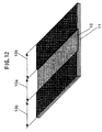
- Fig. 1 is a schematic cross sectional view of an ultrasonic probe of a first embodiment according to the present invention.
- the first embodiment of the present invention is an ultrasonic probe in which a high molecular material layer is provided between a piezoelectric element and an acoustic matching layer, and a conductive layer is disposed on one surface of the high molecular material layer facing to the piezoelectric element so as to be extended out as a GND (ground terminal) of a signal line.
- This first embodiment provides a high quality ultrasonic probe which allows an electrical terminal to be easily extended out of an electrode of the piezoelectric element.
- the first embodiment also allows good sensitivity and frequency characteristics in transmitting and receiving the ultrasonic wave to be secured because the high molecular material also serves as a part of the acoustic matching layer.
- the first embodiment prevents a possible fault caused by a breaking of wire even if the piezoelectric element is cracked by a mechanical impact or the like.
- the piezoelectric probe of the present invention comprises a piezoelectric element 1 for transmitting and receiving the ultrasonic wave, which is made of piezoelectric ceramic including PZT-based material, single crystal or high molecular material such as PVDF (poly-vinylidene fluoride); a ground electrode 3 formed on one surface of the piezoelectric element by depositing or sputtering gold or silver thereon or by baking silver thereon; a positive electrode 2 formed on the other surface of the piezoelectric element by depositing or sputtering gold or silver thereon or by baking silver thereon same as the ground electrode 3; a signal electrical terminal 4 extended out of the positive electrode 2; a backing material 9 for mechanically holding the piezoelectric element 1 and for functioning to damp undesired ultrasonic signal; a high molecular material layer 11 having high molecular material as base material and being provided on the ground electrode 3 of the piezoelectric element 1; a conductive layer 10 made of conductive material provided on one surface of piezoelectric ceramic including
- This ultrasonic probe transmits and receives the ultrasonic wave by applying an electrical signal from a main body of an ultrasonic diagnostic apparatus through the signal electrical terminal 4 and the conductive layer 10 or GND (ground terminal) to the piezoelectric element 1 and thereby inducing the piezoelectric element 1 to be vibrated mechanically.
- An ultrasonic probe of an ultrasonic diagnostic apparatus for diagnosing a human body as a subject to be examined is a so-called sensor used for diagnosing the human body, which is brought into direct contact with the human body, transmits the ultrasonic wave into the human body, and receives a reflected wave reflected from the human body, so that the signal of the reflected wave is processed at the main body of the apparatus and an image for diagnosis is displayed on a monitor.
- the ground electrode 3 provided on the piezoelectric element 1 and the conductive layer 10 provided on the high molecular material layer 11 are electrically connected to each other by a method using a conductive adhesive or a so-called ohmic contact method using a very thin epoxy resin layer.
- the high molecular material layer 11 having the conductive layer 10 formed thereon is eventually folded along a side face of the backing material 9 to be made slim as a whole so as to facilitate an easy operation. Accordingly, the high molecular material layer 11 with the conductive layer 10 formed thereon shall be made thinner because, if it is thick, it can not be folded exactly along the side face of the backing material 9 so as to make a slim shape as a whole.
- the thickness of the high molecular material layer 11 shall be less than 0.05 mm. This high molecular material layer 11 shall not degrade the performance of transmitting and receiving the ultrasonic wave and is preferably as thin as possible so as not to substantially affect the performance.
- the present embodiment has a feature that this high molecular material layer 11 is designed to perform the same function as the acoustic matching layer 7. That is, the materials of the high molecular material layer 11 and the acoustic matching layer 7 are selected so as to have substantially the same acoustic impedance and the total thickness of the high molecular material layer 11, and the acoustic matching layer 7 is adjusted to be about a quarter wavelength of the setting frequency, so that the high molecular material layer 11 can function as a kind of acoustic matching layer without affecting or degrading the performance of transmitting and receiving the ultrasonic wave or the sensitivity and the frequency characteristic.
- Preferable materials used as the high molecular material layer 11 are polyimide, polyethylene-terephthalate, polysulphon, polycarbonate, polyester, polystyrene, polyphenylene-sulphide and the like.
- the acoustic impedance of these materials is within the range of 3 to 4 MRayl.
- the acoustic matching layer 7 the same materials as of the high molecular material layer 11 may be employed, and also other materials may be employed which is close to them especially in the acoustic impedance such as epoxy resin or polyurethane resin having an acoustic impedance of 2.5 to 4 MRayl.
- the thickness of polyimide 0.05 mm at the frequency of 3.5 MHz is equal to 1/12.25 wavelength (0.08 wavelength).
- the thickness of the epoxy resin should be 1/5.88 wavelength (0.17 wavelength) or 0.121 mm, and the total thickness of the high molecular material layer 11 of polyimide and the acoustic matching layer 7 of epoxy resin should be adjusted to a quarter wavelength (0.25 wavelength).
- the conductive layer 10 formed on the high molecular material layer 11 causes no problem at all since the thickness thereof is a few ⁇ m and thereby it hardly affects the performance thereof.
- the piezoelectric element of the first embodiment of the present invention can be formed into a slim shape which is easy to operate without degrading the performance. Further, an ultrasonic probe of high quality can be provided since the structure thereof causes no electrical problem due to a breakage of wire even if the piezoelectric element is cracked by a mechanical impact or the like.
- Fig. 2 is a schematic cross sectional view of an ultrasonic probe of a second embodiment according to the present invention.
- the second embodiment of the present invention is an ultrasonic probe in which a high molecular material layer having a conductive layer formed thereon is a first acoustic matching layer provided on one electrode surface of a piezoelectric element and a second acoustic matching layer so as for the conductive layer to be electrically connected to the first acoustic matching layer, wherein the acoustic impedance of the high molecular material layer is substantially equal to that of the second acoustic matching layer.
- This second embodiment provides a high quality ultrasonic probe which allows an electrical terminal to be easily extended out of an electrode of the piezoelectric element, and also allows good sensitivity and frequency characteristics in transmitting and receiving the ultrasonic wave to be secured because the high molecular material also serves as a part of the acoustic matching layer.
- the second embodiment further prevents a possible fault caused by a breaking of wire even if the piezoelectric element is cracked by a mechanical impact or the like.
- the ultrasonic probe of the second embodiment of the present invention has a piezoelectric element 1, a ground electrode 3, a positive electrode 2, a signal electrical terminal 4, a backing material 9, a high molecular material layer 11, and a conductive layer 10.
- the ultrasonic probe of the present embodiment has a first acoustic matching layer 7a provided on a piezoelectric element 1 side, and a second acoustic matching layer 7b provided on the high molecular material layer 1]
- the first acoustic matching layer 7a and the second acoustic matching laye 7b are provided to improve the efficiency of transmitting and receiving th ultrasonic wave by the piezoelectric element 1, and in this second embodiment, this first acoustic matching layer 7a is made of conductive material configured to be electrically connected to the ground electrode 2 of the piezoelectric element by a bonding method such as ohmic contact or the like.
- the first acoustic matching layer 7a may be made of insulating material if it is provided with a conductive layer in the vicinity of the first acoustic matching layer 7a by a certain method such as deposition or plating so as to be electrically connected to the ground electrode 3 of the piezoelectric element 1.
- the high molecular material layer 11 having the conductive layer 10 formed thereon is bonded onto a surface of the first acoustic matching layer 7a by a bonding method such as ohmic contact so that the conductive layer 10 is brought into contact with the surface of the first acoustic matching layer 7a and thereby the high molecular material layer 11 is electrically connected through the first acoustic matching layer 7a to the ground electrode 3 of the piezoelectric element 1.
- the second acoustic matching layer 7b is provided on other surface of the high molecular material layer 11 by bonding, injection or the like.
- an acoustic lens for focusing ultrasonic beam and for being brought into contact with a subject to be examined is sometimes provided on the acoustic matching layer 7 (not shown).
- the high molecular material layer 11 is designed so as to perform a similar function with that of the second acoustic matching layer 7b, as in the first embodiment. That is, the materials of the high molecular material layer 11 and the second acoustic matching layer 7b are selected so as to have nearly the same acoustic impedance, and the total thickness of the high molecular material layer 11 and the second acoustic matching layer 7b is adjusted to be about a quarter wavelength of the ultrasonic wave at the setting frequency, so that the high molecular material layer 11 may not affect or degrade the performance of transmitting and receiving the ultrasonic wave or the sensitivity and the frequency characteristic.
- Preferable materials used as the high molecular material layer 11 are polyimide, polyethylene-terephthalate, polysulphon, polycarbonate, polyester, polystyrene, polyphenylene-sulphide and the like.
- the acoustic impedance of these materials is within the range of 3 to 4 MRayl.
- the second acoustic matching layer 7b the same materials as of the high molecular material layer 11 may be employed, and also other materials may be employed which has a similar acoustic impedance, such as epoxy resin or polyurethane resin having an acoustic impedance of 2.5 to 4 MRayl.
- the polyimide thickness of 0.05 mm at the frequency of 3.5 MHz is equal to 1/12.25 wavelength (0.08 wavelength).
- the thickness of the epoxy resin should be 1/5.88 wavelength (0.17 wavelength) or 0.121 mm, and the total thickness of the high molecular material layer 11 of polyimide and the second acoustic matching layer 7b of epoxy resin should be adjusted to a quarter wavelength (0.25 wavelength).
- the conductive layer 10 formed on the high molecular material layer 11 causes no problem at all since the thickness thereof is a few ⁇ m and thereby it hardly affects the performance thereof.
- the material employed as the high molecular material layer 11 and that employed as the second acoustic matching layer 7b are similar in their acoustic impedance, a similar effect can also be obtained in other cases where the material employed as the high molecular material layer 11 has an acoustic impedance between those of the first acoustic matching layer 7a and the second acoustic matching layer 7b or has another acoustic impedance substantially equal to that of the first acoustic matching layer 7a.
- the material employed as the high molecular material layer 11 and that employed as the second acoustic matching layer 7b are similar in their acoustic impedance is described, a similar effect can also be obtained in other case where the material employed as the high molecular material layer 11 has an acoustic impedance substantially equal to that of the first acoustic matching layer 7a and the total thickness of the first acoustic matching layer 7a and the high molecular material layer 11 is adjusted to be about a quarter wavelength.
- the piezoelectric element according to the second embodiment can be formed into a slim shape easy to operate without degrading the performance such as the sensitivity and the frequency characteristic. Further, an ultrasonic probe of high quality can be provided since the structure thereof causes no electrical problem due to a breakage of wire even if the piezoelectric element is cracked by a mechanical impact or the like.
- Fig. 3 is a schematic cross sectional view of an ultrasonic probe of a third embodiment according to the present invention.
- the third embodiment of the present invention provides a ultrasonic probe which allows an electrical terminal to be easily extended out of an electrode of the piezoelectric element, and also allows good sensitivity and frequency characteristics in transmitting and receiving the ultrasonic wave to be secured because the high molecular material also serves as a part of the acoustic matching layer.
- the third embodiment further makes it possible to reduce a noise since a shield effect is enhanced by a conductive layer formed on a face of a high molecular material layer located on an acoustic matching layer side.
- the ultrasonic probe of the third embodiment of the present invention has a piezoelectric element 1, a ground electrode 3, a positive electrode 2, a signal electrical terminal 4, a backing material 9, a high molecular material layer 11, a conductive layer 10, a first acoustic matching layer 7a located on the piezoelectric element 1 side, and a second acoustic matching layer 7b provided on the high molecular material layer 11.
- a conductive layer 12 for shielding is provided between the high molecular material layer 11 and the second acoustic matching layer 7b.
- the conductive layer 12 is directly formed on the high molecular material layer 11 by such method as deposition, sputtering, or plating with copper, nickel, silver, gold or the like.
- the conductive layer 12 may be formed on the second acoustic matching layer 7b side by the same method.
- this conductive layer 12 is not electrically connected to the conductive layer 10 which is electrically connected to the ground electrode 3 of the piezoelectric element 1, but is electrically connected to a shield line of a cable which connects the ultrasonic prove to the main body.
- the conductive layer 12 with a thickness of this order causes no problem at all.
- an ultrasonic probe configured as described above allows an image obtained from an ultrasonic diagnostic apparatus to be of higher resolution and of higher sensitivity, and further, provides an ultrasonic probe capable of reducing a noise, since the conductive layer 12 works as a shield.
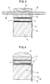
- Fig. 4 is a schematic cross sectional view of an ultrasonic probe of a fourth embodiment of the present invention.
- a piezoelectric element 1 is made of piezoelectric ceramic including PZT-based material, single crystal, or high molecular material such as PVDF (poly-vinylidene fluoride) to be used for transmitting and receiving the ultrasonic wave.
- Each of electrodes 2, 3 is provided on each face of the piezoelectric element 1 respectively. These electrodes 2, 3 are formed by such method as sputtering, deposition, or baking with a metal such as gold, silver or the like.
- An acoustic matching layer 7 is provided on one electrode 3 of the piezoelectric element 1.
- This acoustic matching layer is composed of one or more layers mainly made of resin or graphite for achieving an acoustic matching between the piezoelectric element 1 and a subject to be examined (human body, not shown).
- An acoustic lens 8 is provided on the acoustic matching layer 7. This acoustic lens is mainly made of silicone rubber for converging, diverging and deflecting the ultrasonic wave.
- a signal electrical terminal 4 is provided on the other electrode 2 of the piezoelectric element 1.
- the signal electrical terminal 4 comprises a conductive layer 5 contacting with the electrode 2 of the piezoelectric element 1, and an insulator 6 located on the other side of the conductive layer 5 with respect to the electrode 2.
- the conductive layer 5 is formed by laminating a conductive material such as metal or the like on the insulator 6 using method such as sputtering, deposition, baking or the like.
- the conductive layer 5 is electrically connected to the piezoelectric element 1.
- a backing material 9 is provided on the insulator 6 of the signal electrical terminal 4.
- the backing material 9 is made of epoxy resin or ferrite-mixed rubber and is bonded to the insulator 6 so as to provide a damping effect to the piezoelectric element 1 and also to mechanically support it.
- the signal electrical terminal 4 is laterally extended out of a connecting portion of the piezoelectric element 1 and the backing material 9, and then is folded along a side face of the backing material 9.
- the piezoelectric element 1 In order to electrically connect the piezoelectric element 1 to the conductive layer 5 of the signal electrical terminal 4, they are bonded to each other by a bonding method using a conductive adhesive or by the so-called ohmic contact method using a very thin bonding layer of epoxy resin.
- the signal electrical terminal 4 In order to avoid adversary affect on the damping effect of the backing material 9 for the piezoelectric element 1, the signal electrical terminal 4 must be thin enough.
- the conventional conductive layer 5 employed in ultrasonic probe with, for example, a setting frequency of 3.5 MHz has a thickness less than 1/400 wavelength, and accordingly substantially do not adversary affect on the acoustic characteristic of the ultrasonic probe.
- the insulator 6 of the signal electrical terminal 4 is thick, it affects the acoustic characteristic. Accordingly, the thickness of the insulator 6 must be thin enough so as not to affect the acoustic characteristic.
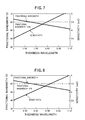
- Fig. 5 shows a calculation result of an acoustic characteristic when the thickness of the insulator 6 is varied in the example 4 with a setting frequency of the ultrasonic wave being set to 3.5 MHz.
- the horizontal axis designates a numerical value calculated by dividing the thickness of the insulator 6 by the ultrasonic wavelength.
- the second vertical axis designates a sensitivity value in which the larger sensitivity value means the higher sensitivity of the ultrasonic probe.
- the dotted line designates a level where the fractional bandwidth is reduced by 5% from the case where the thickness of the insulator 6 is 0 mm.
- Fig. 5 clearly shows that as the thickness of the insulator 6 increases, the sensitivity is improved while the fractional bandwidth is reduced.
- the degradation in the resolution causes no problem if the difference is not observable in the ultrasonic image.
- This unobservable level causing no problem is within a range of about -7.5% degradation in the characteristic of fractional bandwidth, and this value shall be accomplished as a whole ultrasonic probe including the variances in respective materials and respective bonded layers.
- the degradation in the fractional bandwidth caused by the thickness of the insulator 6 shall be reduced further.
- the thickness of the insulator 6 shall be thin enough so that the degradation in the fractional bandwidth is less than -5% compared with the case where the thickness of the insulator 6 is 0 mm.
- Fig. 5 shows that the thickness of the insulator shall be less than 1/25 wavelength of the ultrasonic wavelength in order to make the fractional bandwidth degradation smaller than -5% compared with the case where the thickness of the insulator 6 is 0 mm.
- Fig. 6 is a graph illustrating a calculation result of a frequency characteristic when the central frequency of the ultrasonic probe using the insulator 6 of the example 1 is set to 3.5 MHz.
- Fig. 6 shows the normalized sensitivity for transmitting and receiving the ultrasonic wave as a function of the driving frequency.
- Fig. 6 shows three cases where the thickness of the insulator 6 is 0mm, equal to or smaller than 1/25 wavelength (1/25 wavelength), or equal to or larger than 1/25 wavelength (1/10 wavelength).
- Fig. 6 shows that the fractional bandwidth is about 62% when the thickness of the insulator 6 is 0mm, is about 61% when it is equal to or less than 1/25 wavelength (1/25 wavelength), and is about 53% when it is equal to or larger than 1/25 wavelength (1/10 wavelength).
- the fractional bandwidth of the ultrasonic probe is reduced when an insulator 6 having a thickness equal to or more than 1/25 wavelength is employed.
- the thickness of the insulator 6 is controlled to be equal to or smaller than 1/25 wavelength, the sensitivity of an ultrasonic probe for transmitting and receiving the ultrasonic wave can be improved and also a good frequency characteristic can be obtained.
- polyimide was employed as a material for the insulator 6 in the example 1, other material such as polyethylene-terephthalate, poly-sulphon, polycarbonate, polyester, polystyrene, or poly-phenylene-sulphide can also be employed.
- an ultrasonic probe structured as shown in Fig. 4 was manufactured using polyethylene-terephthalate as the insulator 6.
- the piezoelectric element 1 and the backing material 9 are similar to those of the example 4.
- Fig. 7 shows a calculation result of an acoustic characteristic when the thickness of the insulator 6 is varied in the example 2 with a setting frequency of 3.5 MHz.
- an ultrasonic probe structured as shown in Fig. 4 was manufactured using poly-sulphon as the insulator 6.
- Fig. 8 shows a calculation result of an acoustic characteristic when the thickness of the insulator 6 is varied in the example 3 with a setting frequency of 3.5 MHz.
- both Figs. 7 and 8 show that the thickness of the insulator 6 shall be equal to or smaller than 1/25 wavelength in order to keep the reduction of the fractional bandwidth to be equal to or smaller than 5% compared with the case where the thickness of the insulator 6 is 0 mm.
- the sensitivity of an ultrasonic probe in transmitting and receiving the ultrasonic wave can be improved while keeping a good resolution and a good frequency characteristic.
- the acoustic impedance of the material such as polyimide, polyethylene-terephthalate, poly-sulphon, polycarbonate, polyester, polystyrene, or poly-phenylene-sulphide is within the range of 2 to 4 MRayl.
- the material of the piezoelectric element 1 is selected to have the acoustic impedance of about 30 MRayl and that of the backing material 9 is selected to have the acoustic impedance of about 5 to 10 Mrayl, it is preferable that the thickness of the insulator 6 is adjusted to be equal to or smaller than 1/25 wavelength and also the acoustic impedance thereof is less than the acoustic impedances of the piezoelectric element 1 and the backing material 9.
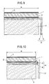
- Fig. 9 is a partial enlarged cross sectional view of the ultrasonic probe of the fourth embodiment of the present invention shown in Fig. 4, illustrating a piezoelectric element, a backing 9 and a signal electric terminal 4 thereof.
- the insulator 6 of the signal electrical terminal 4 shall have a thickness equal to or smaller than 1/25 of the ultrasonic wavelength in the portion (portion A) facing to an ultrasonic wave emitting surface of the piezoelectric element 1.
- the thickness of the insulator need not be controlled because the extended-out portion does not affect the acoustic impedance of the ultrasonic probe.
- the piezoelectric element 1, the signal electrical terminal 4, and a part of the backing material 9 are divided by machining or the like in order to be formed into a plurality of elements aligned along a scanning direction. Accordingly, it is not necessary to apply patterning to the portion A of the conductive layer 5. Further, if the signal electrical terminal 4 is attached to an ultrasonic wave emitting surface of the piezoelectric element 1 covering wide area thereof as much as possible, the electrical connection is impaired little even if the piezoelectric element 1 is cracked by an external mechanical impact, and thereby the ultrasonic probe is less likely to fail and the electrical signal can be transmitted and received well.
- the ultrasonic probe structured according to the fourth embodiment can achieve a highly sensitive acoustic characteristic without degrading the frequency characteristic thereof. Further, the high quality ultrasonic probe can be provided since the structure thereof causes no electrical problem by a possible breakage of wire even if the piezoelectric element is cracked by a mechanical impact or the like.
- Fig. 10 is an enlarged cross sectional view of an ultrasonic probe of a fifth embodiment according to the present invention, which corresponds to Fig. 9 of the fourth embodiment.
- a signal electrical terminal is divided into a first signal electrical terminal 4 disposed between a piezoelectric element 1 and a backing material 9, and a second signal electrical terminal 13 disposed outside a connecting portion of the piezoelectric element 1 and the backing material 9.
- the piezoelectric element 1 and the backing material 9 are similar to those of the fourth embodiment.
- a first signal electrical terminal 4 is provided on an electrode 2 of the piezoelectric element 1.
- the first signal electrical terminal 4 comprises a conductive layer 5 contacting with the electrode 2 of the piezoelectric element 1, and an insulator 6.
- the conductive layer 5 is formed on the insulator 6 by attaching the conductive material such as metal thereon using such method as sputtering, deposition, baking or the like.
- the conductive layer 5 is electrically connected to the piezoelectric element 1.
- the insulator 6 is bonded to the backing material 9.
- the second signal electrical terminal 13 is disposed outside the connecting portion of the piezoelectric element 1 and the backing material 9.
- the second signal electrical terminal 13 is formed by attaching a patterned conductive material onto an insulator using such method as sputtering, deposition, baking or the like.
- the piezoelectric element 1 In order to electrically connect the piezoelectric element 1 to the conductive layer 5 of the first signal electrical terminal 4, they are bonded to each other by the bonding method using a conductive adhesive or by the so-called ohmic contact method using a very thin bonding layer of epoxy resin.
- portion A In order to connect the conductive layer 5 of the first signal electrical terminal 4 to the conductive layer of the second signal electrical terminal 13 in a portion located out of the ultrasonic wave emitting surface (portion A), they are bonded to each other by the bonding method using a conductive adhesive or by the so-called ohmic contact method using a very thin bonding layer of epoxy resin.
- the sensitivity of the ultrasonic probe for transmitting and receiving the ultrasonic wave can be improved and simultaneously a good frequency characteristic can be obtained by, as in the fourth embodiment, adjusting the thickness of the insulator 6 of the first signal electrical terminal 4 to be equal or smaller than 1/25 wavelength. Further, the thickness of the insulator 6 need not be controlled in the area other than that covering the ultrasonic wave emitting surface (portion A) since the acoustic impedance of the ultrasonic probe is not affected thereby.
- preferable material employable as the insulator 6 is polyimide, polyethylene-terephthalate, poly-sulphon, polycarbonate, polyester, polystyrene, poly-phenylene-sulphide or the like.
- the acoustic impedance of polyimide, polyethylene-terephthalate, poly-sulphon, polycarbonate, polyester, polystyrene, poly-phenylene-sulphide or the like is within the range of 2 to 4 MRayl.
- the material of the piezoelectric element 1 is selected to have the acoustic impedance of about 30 MRayl and that of the backing material 9 is selected to have about 5 to 10 Mrayl, it is preferable that the thickness of the insulator 6 is adjusted to be equal to or smaller than 1/25 wavelength, and also the acoustic impedance thereof is smaller than the acoustic impedances of the piezoelectric element 1 and the backing material 9.
- the piezoelectric element 1, the signal electrical terminal 4, and a part of the backing material 9 are divided by machining or the like. Accordingly, it is not necessary to apply patterning to the portion A of the conductive layer 5. Further, if the signal electrical terminal 4 is attached to an ultrasonic wave emitting surface of the piezoelectric element 1 covering wide area thereof as much as possible, the electrical connection is impaired little even if the piezoelectric element 1 is cracked by an external mechanical impact, and thereby the ultrasonic probe is less likely to fail and the electrical signal can well be transmitted and received.
- the ultrasonic probe of the fifth embodiment also can achieve a highly sensitive acoustic characteristic without degrading the frequency characteristic thereof, as in the case of the ultrasonic probe of the fourth embodiment. Further, the high quality ultrasonic probe can be provided since the structure thereof causes no electrical problem by a possible breakage of wire even if the piezoelectric element is cracked by a mechanical impact or the like.
- the ultrasonic probe of the fifth embodiment since the signal electrical terminal is divided into a first signal electrical terminal (the thickness of which must be precisely controlled) and a second signal electrical terminal (the thickness of which need not be precisely controlled), the first and the second signal electrical terminals having different thickness from each other can be manufactured separately. Accordingly, the ultrasonic probe of the fifth embodiment is advantageous in manufacturing over the first embodiment, the signal electrical terminal of which has portions having different thickness and also is required to be folded.
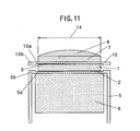
- Fig. 11 shows an ultrasonic probe of a sixth embodiment according to the present invention.
- the piezoelectric element 1 is an electrostrictive element made of piezoelectric ceramic or the like, and the thickness thereof is optimized based on a driving frequency.
- the piezoelectric element 1 is provided, in advance, with a ground electrode 3 on a front face thereof and with a positive electrode 2 on a back face thereof. These electrodes has a thickness of 0.5 to 10 ⁇ m and are formed by such methods as sputtering, deposition or plating with gold, though the material is not limited to gold.
- the piezoelectric element 1 sandwiched between the positive electrode 2 and the ground electrode 3 has an acoustically effective area 14 which is subjected to polarizing action and thereby substantially transmits and receives the ultrasonic wave.
- a ground electrode side conductive layer 10 is provided on a front face of the ground electrode 3 to be electrically connected thereto, and this ground electrode side conductive layer 10 is made of conductive material having a different thickness depending on areas thereof, such that a ground electrode side conductive layer portion 10a (thin portion) covering at least the acoustically effective area 14 has a thickness of 0.5 to 10 ⁇ m while other portion (thick portion) 10b has another thickness of 15 to 50 ⁇ m.
- the ground electrode side conductive layer 10 having the different thickness depending on the areas thereof can be formed by a method comprising the steps of applying a masking in a desired pattern to a copper foil having a thickness of 0.5 to 10 ⁇ m, plating for thickening the conductive layer, and then removing the mask therefrom.
- the ground electrode side conductive layer 10 can also be formed by an alternative method comprising the steps of applying a desired masking to a copper foil having a thickness of 15 to 50 ⁇ m, applying an etching process to make it partially thinner, and then removing the mask therefrom.
- ground electrode side conductive layer 10 is provided, on a front face of thereof, with an acoustic matching layer 7 for making an acoustic matching and an acoustic lens 8 made of such material as silicone rubber for focusing the ultrasonic wave.
- a positive electrode side conductive layer 5 made of such electrically conductive material as copper foil is laminated onto a back face of the positive electrode 2 so as to be electrically connected to the positive electrode 2.
- This positive electrode side conductive layer 5 is, same as the ground electrode side conductive layer 10, made of conductive material having a different thickness depending on areas thereof, such that a positive electrode side conductive layer portion 5a (thin portion) covering at least the acoustically effective area 14 has a thickness of 0.5 to 10 ⁇ m while other portion (thick portion) 5b has another thickness of 15 to 50 ⁇ m.
- the positive electrode side conductive layer 5 can be formed in the similar method employed for the ground electrode side conductive layer 10, and can be provided with a desired pattern in advance, if necessary.
- a backing material 9 is provided on a back face of the positive electrode side conductive layer 5 to complete an ultrasonic probe.
- the thickness of both conductive layers on the positive electrode side and on the ground electrode side is partially varied, the thickness may be partially varied in only one of the positive and the ground electrode side conductive layers, and this is also applied to the case where the conductive layer on either side is partially extended over the acoustically effective area.
- copper is employed as the conductive material in the above description, such conductive materials as silver, nickel, etc. may be employed without being limited to copper.
- there is only one acoustic matching layer there may be employed two or more acoustic matching layers.
- the conductive layer has different thickness such that the area covering the electrode portion of the piezoelectric element is thinner than other area thereof, the acoustic mismatch can be suppressed because of the thin conductive layer within the acoustically effective area 14 where an ultrasonic vibration is actually generated and the acoustic matching is required.
- the electrical signal can be transmitted at a low electrical impedance because of the thick conductive layer at other area of conductive layer used as an electrically conductive path portion.
- the negative effect due to the acoustic mismatch can be limited to an extremely low level when the thickness thereof is equal to or smaller than 1/20 wavelength of the ultrasonic wave to be transmitted and received, and thereby an ultrasonic probe of high sensitivity and high resolution can be provided without degrading the frequency characteristic in transmitting and receiving the ultrasonic wave and the sensitivity by making the thickness of the conductive layer equal to or smaller than 5 ⁇ m within the acoustically effective area 14, though it depends on the designed frequency of the ultrasonic probe.
- the electrical impedance can be controlled to be low by making the conductive layer serving as the electrically conductive path thick, a capacity for removing the external electrical noise can be improved, and thereby an ultrasonic diagnostic image of high sensitivity and high resolution can be provided without any deterioration of the diagnostic image due to the external electromagnetic wave noise.
- the structure described above can simultaneously optimize both acoustic matching condition and electrical conductive path, and can provide information based on an ultrasonic diagnostic image of high accuracy.
- Fig. 12 is a perspective view, illustrating a structure of a conductive layer formed beforehand on a base material layer in place of the conductive layer of the sixth embodiment, wherein the thickness of the conductive layer is partially different from the other parts therein.
- a ground electrode side base material layer 11 is made of, for example, insulating high molecular film of polyimide with a thickness of about 5 to 50 ⁇ m, and a ground electrode side conductive layer 10 having different thickness depending on areas therein is formed on one surface of the base material layer 11.
- This ground electrode side conductive layer 10 has, in the middle part thereof, a ground electrode side conductive layer 10a (thin portion) covering at least an acoustic effective area 14, and other ground electrode side conductive layers 10b (thick portion) disposed on both sides of the thin portion, wherein the thickness of the thin portion is preferably 0.5 to 10 ⁇ m and that of the thick portion is preferably 15 to 50 ⁇ m.
- This ground electrode side conductive layer 10 having the different thickness depending on the areas therein can be formed by a method comprising the steps of forming a copper layer with a thickness of 0. 5 to 10 ⁇ m on a base material layer made of polyimide with a thickness of 5 to 50 ⁇ m by plating, sputtering, etc., applying a masking to an area to be kept thin in a desired pattern, plating areas to be made thick with conductive material so as to be made thicker, and then removing the mask.
- the ground electrode side conductive layer 10 can also be formed by an alternative method comprising the steps of plating a base material of polyimide with copper of 15 to 50 ⁇ m thick, applying a mask to a portion to be kept thick in a desired pattern, partially etching a non-masked portion of the copper to make it thinner, and then removing the mask.
- ground electrode side conductive layers described above is similar to those generally employed in the production of flexible print circuit.
- Fig. 12 shows a structure of the ground electrode side conductive layer having the different thickness depending on the areas, and an electrode side conductive layer has also the same structure. At that time, a desired pattern can be applied to the electrode side conductive layer, if necessary.
- the material of the base material layer is not limited to polyimide, but other materials hard to be plastically deformed may be employed.
- the conductive layer formed on the base material layer provides such a remarkable advantageous effect that, in addition to the operation and effect of the sixth embodiment, the conductive portion formed by the thinner portion of the conductive layer is not likely to be creased, crinkled or eventually plastically deformed, which makes it easy to handle the conductive layer and the ultrasonic probe during the production process thereof.
- Fig. 13 shows an ultrasonic probe of a seventh embodiment according to the present invention.
- the ultrasonic probe of the seventh embodiment comprises a piezoelectric element 1 having a positive electrode on one face thereof and having a ground electrode on the other face thereof; an acoustic matching layer 7 provided on a front face of the ground electrode; a ground electrode side conductive layer 10 provided on a front face of the acoustic matching layer 7, disposed on a ground electrode side base material layer 11, and having a different thickness depending on areas thereof; and an acoustic lens 8 provided on a front face of the ground electrode side conductive layer 10.
- the present invention provides an ultrasonic probe in which the ground electrode side base material layer 11 works as a second acoustic matching layer.
- the acoustic matching layer 7 is made of electrically conductive material such as graphite so as to be electrically connected to the ground electrode 3 provided on the front face of the piezoelectric element 1. Further, as described in Fig. 12, the ground electrode side base material layer 11 and the ground electrode side conductive layer 10 having a different thickness depending on the areas are provided between the acoustic matching layer 7 and the acoustic lens 8. This ground electrode side conductive layer 10 is formed in advance on the ground electrode side base material layer 11 so as to be electrically connected to the acoustic matching layer 7.
- the ground electrode side base material layer 11 is designed to work as an acoustic matching layer. That is, it is preferable that the acoustic impedance of the material of the ground electrode side base material layer 11 is between those of the acoustic matching layer 7 and the acoustic lens 8, and the thickness thereof is about a quarter wavelength of the ultrasonic wave to be transmitted and received.
- ground electrode side base material layer 11 is disposed between the ground electrode 3 and the acoustic matching layer 7, it may cause an acoustic mismatch, depending on the acoustic impedance value of the ground electrode side base material layer 11.
- the ground electrode side base material layer 11 can be positively utilized as a second acoustic layer by optimizing the impedance and the thickness thereof.
- the ultrasonic probe of the seventh embodiment of the present invention not only can avoid the acoustic mismatch but also can optimize the acoustic matching, and thereby an ultrasonic probe of high sensitivity and high resolution can be obtained by improving the sensitivity and the frequency characteristic in transmitting and receiving the ultrasonic wave.
- Preferable materials as the ground electrode side base material layer 11 of the seventh embodiment are high molecular films having an acoustic impedance within the range of 2.5 to 4.5 Mrayl such as polyimide, polyester, polycarbonate or polyethylene.
- Fig. 14 shows an ultrasonic probe of the eighth embodiment of the present invention.
- Fig. 14 is a cross sectional view of an ultrasonic probe, taken along a short axis thereof.
- the word “up” means a direction from the lower part of the drawing to the upper part thereof.
- the piezoelectric element 1 is made of piezoelectric ceramic including PZT-based material, single crystal, or high molecular material such as PVDF. Further, the piezoelectric element 1 is provided with a ground electrode 3 and a positive electrode 2 each disposed on opposite faces thereof respectively.
- the ground electrode 3 and the positive electrode 2 are formed by deposition, plating or sputtering using gold, silver, copper, tin, nickel or aluminum, or by baking with silver.
- a first acoustic matching layer 7a is provided on an upper surface of the piezoelectric element 1 (on the surface facing to a subject to be examined) for efficiently transmitting the ultrasonic wave, and is made of conductive material such as graphite.
- the first acoustic matching layer 7a and the ground electrode 3 of the piezoelectric element 1 are electrically connected to each other by a method using a conductive adhesive or by the so-called ohmic contact method using a very thin layer of epoxy resin.
- a conductive film 17 composed of a base film 15 made of high molecular material and a conductive copper layer 16 is disposed along a side face of a backing material 9 (which will be described later).
- the conductive film 17 is flexible.
- the first acoustic matching layer 7a is electrically connected at both side ends of a lower face thereof to the copper layer 16 of the conductive film 17 by the conductive adhesive. They may be electrically connected also by the insulating resin with the ohmic contact method as described above.
- the ground electrode 3 works as a common electrode for GND.
- the first acoustic matching layer 7a is wider than the piezoelectric element 1, and extends beyond the side of the piezoelectric element 1.
- a second acoustic matching layer 7b is provided on an upper surface of the first acoustic matching layer 7a for efficiently propagating the ultrasonic wave, and is made of epoxy resin or high molecular material such as polyimide, polyethylene-terephthalate, poly-sulphon, polycarbonate, polyester, polystyrene, or poly-phenylene-sulphide.
- an acoustic lens (not shown) made of silicone rubber, urethane rubber or plastics is provided on an upper surface of the second acoustic matching layer 7b via an adhesive for focusing the ultrasonic wave.
- the positive electrode 2 disposed beneath the piezoelectric element 1 is a signal electrode formed as a pattern on, for example, a high molecular material film, and is electrically connected to FPC 4 by a conductive adhesive.
- the backing material 9 is made of ferrite-rubber, epoxy or urethane rubber mixed with micro-balloons for holding the piezoelectric element 1 as well as for absorbing undesired ultrasonic wave.
- an insulating layer 18 is provided in a space formed between an end portion of the acoustic matching layer 7a and that of the backing material 9.
- the insulating layer 18 is made of insulating material such as epoxy resin, and works to insulate the conductive film 17 from the FPC 4 and the positive electrode 2 of the piezoelectric element 1, as well as to support the end portion of the first acoustic matching layer 7a extending out of the piezoelectric element 1.
- a conductive adhesive is used for connecting the conductive film 17 to the first acoustic matching layer 7a and for connecting the positive electrode 2 of the piezoelectric element 1 to the FPC 4, an insulating adhesive may be used also to connect them electrically if it is cured with compressed. It is preferable that a layer of gold or nickel is formed on the surface of the copper layer 16 of the conductive film 17 by deposition, plating or sputtering in order to prevent the oxidation thereof.
- step (A) at first, the ground electrode 3 and the positive electrode 2 are formed on the piezoelectric element 1 in advance.
- the piezoelectric element 1 and the FPC 4 are bonded to each other by applying a conductive adhesive onto the positive electrode 2 of the piezoelectric element 1 and the FPC 4, and heating them while applying pressure to this stacked block of FPC4 and the piezoelectric element 1 to cure the conductive adhesive.
- step (B) the first acoustic matching layer 7a and the conductive film 17 are bonded to each other by applying a conductive adhesive to an end of the first acoustic matching layer 7a and the copper layer 16 of the conductive film 17, and heating them while applying pressure to this stacked block of the first acoustic matching layer 7a and the conductive film 17 to cure the conductive adhesive.
- the conductive film 17 is preferably bonded in its flat condition.
- step (C) the backing material 9, the piezoelectric element 1 with the FPC 4 bonded thereon, the first acoustic matching layer 7a with the conductive film 17 bonded thereon, and the second acoustic matching layer 7b are bonded to one another by adhesive.
- step (D) the insulating layer 18 is formed in a space formed between the end portion of the acoustic matching layer 7a and that of the backing material 9.
- step (E) the bonded members are cut into arrays with a predetermined pitch by a cutting machine such as a dicer.
- step (F) they are bent into a predetermined curvature.
- step (G) they are bonded and fixed to a member made of the same material as of the backing material 9 or of hard material such as epoxy or metal, or a composite plate made by combining these members (not shown).
- step (H) the FPC 4 and the conductive film 17 are bent to form a shape as shown in Fig. 14.
- step (I) the acoustic lens (not shown) is bonded on the second acoustic matching layer 7b by adhesive.
- the above manufacturing method describes how to manufacture a convex type ultrasonic probe, and the same method may be applied to a linear type ultrasonic probe.
- the linear type ultrasonic probe when the end of the first acoustic matching layer 7a and the copper layer 16 of the conductive film 17 are bonded to each other by applying a conductive adhesive thereto, and heating them while applying pressure to the stacked block thereof to cure the conductive adhesive, the conductive film 17 may be bent in advance to form about a right angle before it is bonded. Alternatively, the conductive film 17 may be bent after having been heated to cure the adhesive.
- a plurality of electrical signals transmitted with arbitrary delays in timing from a transmitting section of a main body of an ultrasonic diagnostic apparatus are transmitted through a cable (not shown) and the FPC 4 to a plurality of piezoelectric elements 1 arranged in an array.
- the piezoelectric element 1 to which the electrical signals are transmitted generates the ultrasonic wave, and then the ultrasonic waves propagate through the first acoustic matching layer 7a, the second acoustic matching layer 7b and the acoustic lens (not shown).
- the ultrasonic waves are focused and/or deflected with respect to the scanning direction in response to the timing delay from the transmitting section.
- the ultrasonic waves are propagated into the patient body.
- the ultrasonic waves are reflected at the interfaces of the internal organs of the patient by an acoustic impedance difference.
- the reflected ultrasonic waves are received by the piezoelectric elements 1, converted into electrical signals, and then transmitted through the cable to a receiving section of the main body of the ultrasonic diagnostic apparatus.
- An internal image of the patient can be visualized on a monitor by processing the signals received by the receiving section and by displaying the image of the received signals on a display section of the main body of the ultrasonic diagnostic apparatus. Though these operations are similar to those of a conventional ultrasonic probe, the application of the ultrasonic probe of the present invention is not limited to the transmitting and receiving method employed in the main body described above.
- a layer of gold or nickel is formed on the surface of the copper layer 16 of the conductive film 17 by deposition, plating, or sputtering in order to prevent the oxidation thereof.
- the conductive film 17 may be made of thin layer of copper, aluminum or the like without using a base film 15 of high molecular material.
- the positive electrode 2 of the piezoelectric element 1 is extended out as FPC 4, how to extend out the positive electrode 2 is not limited to this manner.
- the ground electrode 3 is used as a GND electrode and the positive electrode 2 is used as a signal electrode respectively.
- a conductive adhesive layer (not shown) is provided on a side of the first acoustic matching layer 7a to strongly fix the conductive film 17 to the first acoustic matching layer 7a and to increase a bonding area therebetween, a contact resistance may be reduced and a noise generation may be prevented. It can easily manufactured.
- a flexible conductive film 17 facilitates a forming of a curved face after a dice machining in case of, for example, the convex type ultrasonic probe. Further, since an electrical connection can be maintained through the conductive first acoustic matching layer even if the piezoelectric element is cracked by a mechanical impact, there can be provided a high quality ultrasonic probe including a convex probe, a linear probe and a matrix probe, in which the performance of the piezoelectric element is not degraded, a fault due to breaking of wire is less likely to occur, and unwanted radiation hardly takes place.
- a flexible conductive film 17 makes it easy to apply a stable pressure to the bonding face of the first acoustic matching layer, and also provides an advantageous effect that separation due to handling after bonding is not likely to occur and thereby an ultrasonic probe can be easily manufactured.
- the insulating layer 18 in the space formed on the side of the piezoelectric element 1 and between the first acoustic matching layer 7a and the backing material 9, it possible to support the first acoustic matching layer 7a, which strengthen the first acoustic matching layer against a mechanical impact during, for example, the machining process by the dicer, and thereby makes it easy to manufacture the ultrasonic probe.
- the electrical connection between the first acoustic matching layer and the conductive film makes it unnecessary to bond the conductive film to the piezoelectric element using a conductive adhesive of high curing temperature.
- the ultrasonic probe can be easily manufactured without degrading the performance of the piezoelectric element since the piezoelectric element need not be exposed to an environment of high temperature.
- Fig. 15 shows an ultrasonic probe of a ninth embodiment according to the present invention.
- the ninth embodiment is different from the eighth embodiment in that a copper layer 16 of a conductive film 17 is electrically connected to a first acoustic matching layer 7a by a conductive adhesive at both side ends of an upper face of the first acoustic matching layer 7a.
- the piezoelectric element 1, the ground electrode 3, the positive electrode 2, the first acoustic matching layer 7a, the FPC 4, and the backing material 9 are similar to those of the eighth embodiment.
- the piezoelectric element 1 is provided with the ground electrode 3 and the positive electrode 2 on two opposite faces thereof, respectively.
- a first acoustic matching layer 7a is provided on an upper surface of the piezoelectric element 1 for efficiently propagating the ultrasonic wave.
- the first acoustic matching layer 7a and the ground electrode 3 are electrically connected to each other by a method using a conductive adhesive or the so-called ohmic contact method using a very thin layer of epoxy resin.
- a flexible conductive film 17 composed of a base film 15 and a conductive copper layer 16 is disposed on each side of the piezoelectric element 1.
- the copper layer 16 of the conductive film 17 and the first acoustic matching layer 7a are electrically connected to each other at both side ends of an upper surface of the first acoustic matching layer 7a. They may be electrically connected also by an insulating resin with the ohmic contact method.
- the ground electrode 3 is a common electrode for GND.
- the second acoustic matching layer 7b is provide on the upper surface of the first acoustic matching layer 7a for efficiently propagating the ultrasonic wave, and is made of high molecular material such as epoxy resin, polyimide, polyethylene-terephthalate, poly-sulphon, polycarbonate, polyester, polystyrene, or poly-phenylene-sulphide.
- An acoustic lens (not shown) is attached onto an upper surface of the second acoustic matching layer 7b by an adhesive. This acoustic lens is made of silicone rubber, urethane rubber, or plastic for focusing the ultrasonic wave.
- the positive electrode 2 disposed beneath the piezoelectric element 1 is a signal electrode formed as a pattern on, for example, a high molecular material film, and is electrically connected to FPC 4 by a conductive adhesive.
- the backing material 9 is made of such material as ferrite-rubber, epoxy or urethane rubber mixed with micro-balloons for holding the piezoelectric element 1 and for absorbing undesired ultrasonic wave.
- an insulating layer 18 is provided in a space formed between an end portion of the first acoustic matching layer 7a and that of the backing material 9.
- the insulating layer 18 is made of insulating material such as epoxy resin so as to insulate the conductive film 17 from the FPC 4 and the positive electrode 2 of the piezoelectric element 1, and also to support the first acoustic matching layer 7a extended to an area where the piezoelectric element 1 does not exists.
- Fig. 16 shows an ultrasonic probe of the tenth embodiment according to the present invention.
- the tenth embodiment is different from the eighth and the ninth embodiments in the point that a conductive layer 19 electrically connected to the first acoustic matching layer 7a is provided on the second acoustic matching layer 7b provided on an upper surface of the first acoustic matching layer 7a.
- the piezoelectric element 1, the ground electrode 3, the positive electrode 2, the first acoustic matching layer 7a, the conductive film 17, the FPC 4, and the backing material 9 are similar to those of the eighth embodiment.
- the ground electrode 3 and the positive electrode 2 are provided on two opposite faces of the piezoelectric element 1 respectively.
- the first acoustic matching layer 7a is provided on an upper surface of the piezoelectric element 1 for efficiently propagating the ultrasonic wave.
- the conductive film 17 composed of a base film 15 and a conductive copper layer 16 is disposed in each side of the piezoelectric element 1. At both side end portions of the under surface of the first acoustic matching layer 7a, the conductive copper layer 16 of the conductive film 17 and the first acoustic matching layer 7a are electrically connected to each other by a conductive adhesive.
- the second acoustic matching layer 7b is provided on an upper surface of the first acoustic matching layer 7a.
- This second acoustic matching layer 7b has a function to efficiently propagate the ultrasonic wave and is made of high molecular material such as epoxy resin, polyimide, polyethylene-terephthalate, poly-sulphon, polycarbonate, polyester, polystyrene, or poly-phenylene-sulphide.
- a conductive layer 19 electrically connected to the first acoustic matching layer 7a is provided on an under surface of the second acoustic matching layer 7b.
- an acoustic lens (not shown) is attached on an upper surface of the second acoustic matching layer 7b by an adhesive.
- This acoustic lens is made of such material as silicone rubber, urethane rubber, plastics or the like for focusing the ultrasonic wave and has a convex surface on the upper side thereof (on the side facing to a subject to be examined).
- the positive electrode 2 of the piezoelectric element 1 is a signal electrode formed as a pattern on, for example, high molecular material film and is electrically connected to the FPC 4 by a conductive adhesive.
- the backing material 9 is made of such material as ferrite-rubber, epoxy or urethane rubber mixed with micro-balloons for holding the piezoelectric element 1 and for absorbing undesired ultrasonic wave.
- an insulating layer 18 is provided in a space formed between the first acoustic matching layer 7a and the backing material 9.
- This insulating layer 18 is made of insulating material such as epoxy resin so as to insulate the conductive film 17 from the FPC 4 and the positive electrode 2 of the piezoelectric element 1 and also to support the first acoustic matching layer 7a extending to an area where the piezoelectric element 1 does not exists.
- the second acoustic matching layer 7b having the conductive layer 19 electrically connected to the first acoustic matching layer 7a makes it possible to maintain an electrical connection even if the piezoelectric element 1 or the first acoustic matching layer 7a is cracked by an external mechanical impact, and thereby the ultrasonic probe is less likely to fail and a stable quality may be provided.
- the high molecular material is disposed between the piezoelectric element and the acoustic matching layer, and the conductive layer is provided on the piezoelectric element side surface of the high molecular material so as to be electrically extended out therefrom as the GND of the signal line;
- the high molecular material having a conductive layer electrically connected to the first acoustic matching layer is disposed between the conductive first acoustic layer on one electrode surface of the piezoelectric element and the second acoustic matching layer, and the high molecular material has the acoustic impedance substantially equal to that of the second acoustic matching layer;
- the piezoelectric element having two electrodes each disposed on each side thereof, the acoustic matching layer disposed on one electrode surface of the piezoelectric element and the backing material disposed on the other surface of the piezoelectric element, wherein the conductive material electrically connected to the electrode surface of the pie
- the ultrasonic probe can be formed into slim shape easy to operate without degrading the performance such as the sensitivity, the frequency characteristic or the like. Further, the high quality ultrasonic probe can be obtained since this structure causes no electrical problem due to breakage of wire even if the piezoelectric element is cracked by a mechanical impact or the like.
- the alternative ultrasonic probe of the present invention comprises the piezoelectric element having two electrodes disposed on each side thereof, the backing material on one electrode side of the piezoelectric element, and the signal electrical terminal disposed between the piezoelectric element and the backing material, wherein the signal electrical terminal is composed of the insulating material facing to the backing material and the conductive material facing to one electrode surface of the piezoelectric element and electrically connected to the piezoelectric element, and the insulating material of the signal electrical terminal has the thickness smaller than 1/25 wavelength of the ultrasonic wave within the area facing to the ultrasonic wave emitting face.
- This structure allows the ultrasonic probe to have a good sensitivity in transmitting and receiving the ultrasonic wave, a good resolution, and also a good frequency characteristic.
- the alternative ultrasonic probe of the present invention comprises the piezoelectric element having two electrodes disposed on each side thereof, the acoustic matching layer contacting with one electrode surface of the piezoelectric element, and the backing material disposed on the other side of the piezoelectric element, wherein the acoustic matching layer is made of conductive material and is electrically connected to the electrode surface of the piezoelectric element, the end of the acoustic matching layer is electrically connected to the conductive film disposed on the side portion of the backing material, and thereby the one electrode of the piezoelectric element is extended out through the conductive film.
- the structure described above allows the curved surface to be easily formed after the dice machining and further allows the electrical connection to be maintained through the conductive acoustic matching layer even if the piezoelectric element is cracked by the external mechanical impact.
- the piezoelectric element performance is not deteriorated and the ultrasonic probe is less likely to fail and thereby the stable quality can be accomplished.
- an ultrasonic probe of the present invention can be easily manufactured without degrading the performance of the piezoelectric element.
Abstract
Description
- The present invention relates to an ultrasonic probe to be used in an ultrasonic diagnostic apparatus or the like.
- An ultrasonic probe is used, for example, in an ultrasonic diagnostic apparatus for a human body. One of the conventional ultrasonic probes is disclosed in Japanese Patent Laid-Open Publication No. Hei 8-122310. Fig 17 shows a structure of the conventional ultrasonic probe. In Fig. 17, a
piezoelectric element 31 is an element for transmitting and receiving ultrasonic wave, and each face thereof is provided with electrodes. Anacoustic matching layer 37 is made of conductive material and is provided on a face of thepiezoelectric element 31 to efficiently transmit and receive the ultrasonic wave for a subject to be examined (human body). The ultrasonic probe further comprises aconductive layer 40 provided on a highmolecular film 41 by deposition or other proper means so as to be brought into contact with the acoustic matchinglayer 37, anacoustic lens 38 provided on a face of the high molecular film to focus ultrasonic wave, a FPC 34 provided on the other face of thepiezoelectric element 31 so as to form a conductive pattern, and abacking material 39 provided on a face of the FPC 34. This structure allows an electrical connection to be maintained even if thepiezoelectric element 31 is cracked by a mechanical impact from outside, and thereby provides a feature that the piezoelectric element is less likely to fail and a stable quality is provided. - Referring to Fig. 17, the
piezoelectric element 31 is provided with apositive electrode 32 on one face thereof and with aground electrode 33 on the other face thereof. Each of theseelectrodes positive electrode 32 is provided, on a back face thereof, with a laminate of a positive electrode sideconductive layer 35 and a positive electrode sidebase material layer 36 stacked in this order. The positive electrode sidebase material layer 36 is made of high molecular film or the like, and the positive electrode sideconductive layer 35 is formed on this base material layer by plating, sputtering or deposition with metallic material such as copper or gold or by fixing a metal foil thereto, and further is formed into a proper pattern, if necessary. Further, abacking material 39 is provided on a back face of the positive electrode sidebase material layer 36 so that a short pulse characteristic is achieved by braking thepiezoelectric element 31. - Further, a first acoustic matching
layer 37 made of conductive material such as graphite is laminated on a front face of the ground electrode 33 (on the side of a subject to be examined), and further a ground electrode sideconductive layer 40 and a ground electrode sidebase material layer 41 are laminated to a front face of the firstacoustic matching layer 37. - The ground electrode side
base material layer 41 is made of high molecular film or the like, and the ground electrode sideconductive layer 40 is formed on thisbase material layer 41 by plating, sputtering or deposition with such metal as copper or gold or by fixing a metallic foil thereto, where the ground electrode sideconductive layer 40 is disposed below thebase material layer 41 as shown in Fig. 17. Further, anacoustic lens 38 is provided on a front face of the ground electrode sidebase material layer 41 to focus the ultrasonic beam. - In this structure, a mechanical deformation is produced in the
piezoelectric element 31 by an electric signal supplied between the positive electrode sideconductive layer 35 and the ground electrode sideconductive layer 40 from a main body of an ultrasonic diagnostic apparatus (not shown), and thereby a ultrasonic wave is transmitted. - The ultrasonic wave transmitted from this
piezoelectric element 31, after the propagation efficiency thereof into a human body being enhanced by the acoustic matchinglayer 37 and the beam being focused by theacoustic lens 38, is transmitted into the human body (not shown). The ultrasonic beam transmitted into the human body produces a reflective wave when it is reflected by an interface of tissues in the human body. The reflective wave, after passing the same path as the transmitted ultrasonic wave in a reverse direction, is received by thepiezoelectric element 31 and is transformed back into an electric signal to be sent as a received signal to the ultrasonic diagnostic apparatus. Based on this received signal, the ultrasonic diagnostic apparatus forms an image indicative of the information inside of the human body to make a diagnosis. Another conventional ultrasonic probe is disclosed in Japanese Patent Laid-Open Publication No. Hei 11-276479. - Fig. 18 is a schematic perspective view of a conventional ultrasonic probe. In explaining this drawing, the word "up" means a direction from a lower part of the drawing to an upper part thereof. In Fig. 18, a
piezoelectric element 51 is an element for transmitting and receiving the ultrasonic wave. Afirst electrode 53 and asecond electrode 52 each being provided on each face of thepiezoelectric element 51 respectively are electrodes for applying a voltage to thepiezoelectric element 51. Thefirst electrode 53 works as a GND and forms a turning electrode which passes along a side face of the piezoelectric plate extending parallel with a short axis direction thereof and reaches a portion of a face of a backing material of thepiezoelectric element 51. Thefirst electrode 53 of thepiezoelectric element 51 is electrically connected to acopper foil 55, and thesecond electrode 52 is a signal electrode electrically connected to a flexible print circuit (FPC) 54 with a wiring pattern formed thereon. Each electrode is disposed on one of end faces of the piezoelectric element respectively in the short axis direction. Further, thepiezoelectric element 51 and a plurality of acoustic matching layers are cut along a direction parallel with the short axis to form achannel dividing groove 56, so that a plurality of piezoelectric elements are arranged to align with the short axis direction. - A first
acoustic matching layer 57a is provided on an upper face of the first electrode 53 (to be faced to the subject to be examined) so that the ultrasonic wave may be efficiently transmitted and received thereby. A second acoustic matchinglayer 57b is provided on an upper face of the firstacoustic matching layer 57a so that the ultrasonic wave may be efficiently transmitted and received thereby also. Anacoustic lens 58 is provided on the second acoustic matchinglayer 57b to focus the ultrasonic wave. Further, abacking material 59 is provided on a lower face of thesecond electrode 52 in order to absorb undesired ultrasonic wave as well as to hold thepiezoelectric element 51. - In the conventional ultrasonic probe shown in Fig. 17, however, the high
molecular film 41 is provided to be extended out as an electrical terminal and is not contemplated as an acoustic matching layer. Accordingly, there occurs a problem that the efficiency in transmitting and receiving the ultrasonic wave is reduced and further the frequency characteristic is degraded. Further, there is another problem that an insulator of a signal electrical terminal disposed between the piezoelectric element and the backing material is generally thick, which has a negative effect on the damping of the backing material and degrades the acoustic characteristic of the ultrasonic probe, especially the frequency characteristic thereof. - Further, in the conventional ultrasonic probe described above, the acoustic matching
layer 37 is provided in order to efficiently propagate the ultrasonic wave transmitted from the piezoelectric element 31 (generally have a high acoustic impedance of about 25 to 35 Mrayl) into a human body (having an acoustic impedance of about 1.5 Mrayl), and the acoustic matching is optimized by adjusting the acoustic impedance and the thickness of theacoustic matching layer 37, and thereby the ultrasonic having wave of a short pulse length and high propagation efficiency is achieved However, the acoustic matching is impaired and the pulse length and the propagation efficiency are degraded due to an existence of the ground electrode sideconductive layer 40 made of metallic material between the acoustic matchinglayer 37 and theacoustic lens 38. - This problem is also seen at the positive electrode side conductive layer. The conductive layer adversary affect more as the frequency of ultrasonic wave increases.
- The thickness of each conductive layer must be smaller than 5 µm in order to reduce the degradation in the pulse length and the propagation efficiency, while on the other hand, the thinner conductive layer makes the electrical resistance (electrical impedance) larger and thereby a driving electrical signal on an electrical conductive path is lowered to reduce the electrical signal applied to the
piezoelectric element 1, and as a result, the electro-mechanical conversion efficiency from a viewpoint of the diagnostic apparatus is decreased. - Further, when the electrical impedance on the electrical conductive path is increased, the capability of removing external electrical noise is deteriorated, and accordingly the external electromagnetic noise causes the diagnosis image to be deteriorated, which makes the simultaneous optimization of an acoustic matching condition and an electrical conductive path more difficult, and prevents an accurate diagnosis based on the ultrasonic image, and eventually might occur a serious problem of inducing a wrong diagnosis.
- The present invention has been made to solve these problems described above, and the object thereof is, in an ultrasonic probe where the progress toward higher resolution is being developed, to provide diagnostic information based on a highly accurate ultrasonic image by simultaneously optimizing the acoustic matching condition and the electrical conductive path.
- Further, in the conventional system, since the electrodes are disposed on respective end faces of the piezoelectric element with respect to the short axis direction thereof and are extended out therefrom, if the piezoelectric element is subjected to, for example, an external mechanical impact by a post-processing or the like and thereby the first electrode fails to keep an electrical connection due to the breakage thereof, the ability of transmitting and receiving the ultrasonic wave by the piezoelectric element is limited to only a portion of the electrode electrically connected to the copper foil or the FPC, and this sometimes causes to lower the performance of the piezoelectric element. Further, since the copper foil and the FPC are electrically connected by a conductive adhesive or the like at the end faces of the piezoelectric element with respect to the short axis thereof, sometimes another problem occurs that, when a conductive adhesive of high curing temperature is employed, the electrode of the piezoelectric element is deteriorated by heat and thereby the performance of the piezoelectric element is lowered.
- An ultrasonic probe of the present invention has been made to solve these problems. The object of the present invention is to provide a high-quality piezoelectric probe, the performance of which is not degraded even if the piezoelectric element is cracked by a mechanical impact applied thereto.
- The present invention has been made to solve the problems of the conventional system described above. The object of the present invention is to provide a high-quality ultrasonic probe which has the acoustic impedance substantially equal to that of the acoustic matching layer, and does not deteriorate the performance including sensitivity and frequency characteristics. Another object of the present invention is to provide an ultrasonic probe which does not deteriorate the acoustic characteristic, especially the frequency characteristic.
- Further, in the conventional ultrasonic probe described above, there is another problem that an insulator of the signal electrical terminal disposed between the piezoelectric element and the backing material is generally thick, which has a negative effect on the damping performance of the backing material, and degrades the acoustic characteristic of the ultrasonic probe, especially the frequency characteristic thereof.
- The present invention has been made to solve these problems, and the object of the present invention is to provide an ultrasonic probe which does not deteriorate the acoustic characteristic, especially of the frequency characteristic.
- In order to solve the problems described above, the present invention provides an ultrasonic probe in which a high molecular material layer including a conductive layer is disposed on a piezoelectric element, and an acoustic matching layer is disposed on said high molecular material layer, wherein said high molecular material layer has an acoustic impedance substantially equal to that of said acoustic matching layer and the total thickness of these two layers is substantially equal to a quarter wavelength of the ultrasonic wave.
- In an alternative ultrasonic probe of the present invention, a high molecular material layer including a conductive layer is disposed on a first acoustic matching layer, and a second acoustic matching layer is disposed on said high molecular material layer, wherein said high molecular material layer has an acoustic impedance substantially equal to that of said second acoustic matching layer and the total thickness of these two layers is substantially equal to a quarter wavelength of the ultrasonic wave.
- In an alternative ultrasonic probe of the present invention, a conductive layer electrically connected to an electrode face of an piezoelectric element is disposed between said electrode face of the piezoelectric element and an acoustic matching layer, and a high molecular material layer including a conductive layer formed thereon is disposed on the acoustic matching layer side, wherein said high molecular material layer has an acoustic impedance substantially equal to that of said acoustic matching layer and the total thickness of these two layers is substantially equal to a quarter wavelength of the ultrasonic wave.
- In an alternative ultrasonic probe of the present invention, a high molecular material layer is disposed between a first acoustic matching layer and a second acoustic matching layer located on a subject side, wherein an acoustic impedance of said high molecular material layer is between that of said first acoustic matching layer and that of said second acoustic matching layer, or is substantially equal to that of said first acoustic matching layer or that of said second acoustic matching layer.
- Because of these structures described above, the sensitivity of transmitting and receiving the ultrasonic wave can be improved and further, desired frequency characteristic can be provided. Accordingly, an ultrasonic diagnostic apparatus with an image of higher resolution and higher sensitivity can be provided, and also an ultrasonic probe which is less likely to fail and has a stable quality can be obtained since an electrical connection can be maintained even if the piezoelectric element is cracked by an external mechanical impact.
- An alternative ultrasonic probe of the present invention includes a high molecular material layer disposed on a piezoelectric element and an acoustic matching layer disposed on said high molecular material layer, said high molecular material layer comprising a base material made of high molecular material and a conductive layer made of conductive material, wherein said high molecular material layer has an acoustic impedance substantially equal to that of said acoustic matching layer, and thereby the sensitivity of transmitting and receiving the ultrasonic wave can be improved and desired frequency characteristic can be provided. Accordingly, an ultrasonic diagnostic apparatus with an image of higher resolution and higher sensitivity can be provided, and also an ultrasonic probe which is less likely to fail and has a stable quality can be obtained since an electrical connection can be maintained even if the piezoelectric element is cracked by an external mechanical impact.
- Further, an alternative ultrasonic probe of the present invention includes a high molecular material layer disposed on a piezoelectric element and an acoustic matching layer disposed on said high molecular material layer, said high molecular material layer comprising a base material made of high molecular material and a conductive layer made of conductive material, wherein said high molecular material layer has an acoustic impedance substantially equal to that of said acoustic matching layer and the total thickness of these two layers is substantially equal to a quarter wavelength of the ultrasonic wave, and thereby the sensitivity of transmitting and receiving the ultrasonic wave can be improved and further desired frequency characteristic can be provided. Accordingly, an ultrasonic diagnostic apparatus with an image of higher resolution and higher sensitivity can be provided, and also an ultrasonic probe which is less likely to fail and has a stable quality can be obtained since an electrical connection can be maintained even if the piezoelectric element is cracked by an external mechanical impact.
- Further, an alternative ultrasonic probe of the present invention includes a high molecular material layer disposed on a piezoelectric element and an acoustic matching layer disposed on said high molecular material layer, said high molecular material layer comprising a base material made of high molecular material and a conductive layer made of conductive material, wherein said high molecular material is made of polyimide, polyethylene-terephthalate, polysulphon, polycarbonate, polyester, polystyrene, poly-phenylene-sulphide or the like, and said high molecular material layer has an acoustic impedance substantially equal to that of said acoustic matching layer, and thereby the sensitivity of transmitting and receiving the ultrasonic wave can be improved and further desired frequency characteristic can be provided. Accordingly, an ultrasonic diagnostic apparatus with an image of higher resolution and higher sensitivity can be provided, and also an ultrasonic probe which is less likely to fail and has a stable quality can be obtained since an electrical connection can be maintained even if the piezoelectric element is cracked by an external mechanical impact.
- Further, an alternative ultrasonic probe of the present invention includes a high molecular material layer disposed on a first acoustic matching layer and a second acoustic matching layer disposed on said high molecular material layer, said high molecular material layer comprising a base material made of high molecular material and a conductive layer made of conductive material, wherein said high molecular material layer has an acoustic impedance substantially equal to that of said second acoustic matching layer, and thereby the sensitivity of transmitting and receiving the ultrasonic wave can be improved and further desired frequency characteristic can be provided. Accordingly, an ultrasonic diagnostic apparatus with an image of higher resolution and higher sensitivity can be provided, and also an ultrasonic probe which is less likely to fail and has a stable quality can be obtained since an electrical connection can be maintained even if the piezoelectric element is cracked by an external mechanical impact.
- Further, an alternative ultrasonic probe of the present invention includes a high molecular material layer disposed on a first acoustic matching layer and a second acoustic matching layer disposed on said high molecular material layer, said high molecular material layer comprising a base material made of high molecular material and a conductive layer made of conductive material, wherein said high molecular material layer has an acoustic impedance substantially equal to that of said second acoustic matching layer, and the total thickness of these two layers is substantially equal to a quarter wavelength of the ultrasonic wave, and thereby the sensitivity of transmitting and receiving the ultrasonic wave can be improved and further desired frequency characteristic can be provided. Accordingly, an ultrasonic diagnostic apparatus with an image of higher resolution and higher sensitivity can be provided, and also an ultrasonic probe which is less likely to fail and has a stable quality can be obtained since an electrical connection can be maintained even if the piezoelectric element is cracked by an external mechanical impact.
- Further, an alternative ultrasonic probe of the present invention includes a high molecular material layer disposed on a first acoustic matching layer and a second acoustic matching layer disposed on said high molecular material layer, said high molecular material layer comprising a base material made of high molecular material and a conductive layer made of conductive material, wherein said high molecular material is made of polyimide, polyethylene-terephthalate, polysulphon, poly-carbonate, polyester, polystyrene, poly-phenylene-sulphide or the like, and said high molecular material layer has an acoustic impedance substantially equal to that of said second acoustic matching layer, and thereby the sensitivity of transmitting and receiving the ultrasonic wave can be improved and further desired frequency characteristic can be provided. Accordingly, an ultrasonic diagnostic apparatus with an image of higher resolution and higher sensitivity can be provided, and also an ultrasonic probe which is less likely to fail and has a stable quality can be obtained since an electrical connection can be maintained even if the piezoelectric element is cracked by an external mechanical impact.
- Further, an alternative ultrasonic probe of the present invention includes a first conductive layer which is made of conductive material and is disposed between an electrode face of a piezoelectric element and an acoustic matching layer so as to be electrically connected to said electrode face of the piezoelectric element, and a high molecular material layer disposed on said acoustic matching layer side, said high molecular material layer comprising a base material made of high molecular material and a second conductive layer made of conductive material, wherein said high molecular material layer has an acoustic impedance substantially equal to that of said acoustic matching layer, and thereby the sensitivity of transmitting and receiving the ultrasonic wave can be improved and further desired frequency characteristic can be provided. Accordingly, an image on an ultrasonic diagnostic apparatus may be improved to be of higher resolution and of higher sensitivity, and further a noise can be reduced since the conductive material works as a shield.
- Further, an alternative ultrasonic probe of the present invention includes a conductive layer which is made of conductive material and is disposed between an electrode face of a piezoelectric element and an acoustic matching layer so as to be electrically connected to said electrode face of the piezoelectric element, and a high molecular material layer disposed on said acoustic matching layer side, said high molecular material layer comprising a base material made of high molecular material and a conductive layer made of conductive material, wherein said high molecular material layer has an acoustic impedance substantially equal to that of said acoustic matching layer, and thereby the sensitivity of transmitting and receiving the ultrasonic wave can be improved and further desired frequency characteristic can be provided. Accordingly, an image on an ultrasonic diagnostic apparatus may be improved to be of higher resolution and of higher sensitivity, and further a noise can be reduced since the conductive material works as a shield.
- Further, an alternative ultrasonic probe of the present invention includes a first acoustic matching layer located on a piezoelectric element side, a second acoustic matching layer located on a subject side, and a high molecular material layer between said first acoustic matching layer and said second acoustic matching layer, said high molecular material layer comprising a base material made of high molecular material and a conductive layer made of conductive material, wherein an acoustic impedance of said high molecular material layer is between those of said first acoustic matching layer and said second acoustic matching layer or substantially equal to that of said first acoustic matching layer or said second acoustic matching layer, and thereby the sensitivity of transmitting and receiving the ultrasonic wave can be improved and further desired frequency characteristic can be provided. Accordingly, an ultrasonic diagnostic apparatus with an image of higher resolution and higher sensitivity can be provided, and also an ultrasonic probe which is less likely to fail and has a stable quality can be provided since an electrical connection can be maintained even if the piezoelectric element is cracked by an external mechanical impact.
- Further, an alternative ultrasonic probe of the present invention comprises a piezoelectric element having electrodes on both sides thereof, a backing material on one electrode side of said piezoelectric element, and a signal electrical terminal between said piezoelectric element and said backing material, said signal electrical terminal comprising an insulator facing to said backing material and a conductive material facing to one electrode face of said piezoelectric element so as to be electrically connected to said piezoelectric element, wherein said insulator of said signal electrical terminal has a thickness equal to or less than 1/25 wavelength of an ultrasonic wave at an area facing to an ultrasonic wave emitting surface of said piezoelectric element.
- Because of the structure described above, there can be provided an ultrasonic probe having an improved sensitivity for transmitting and receiving the ultrasonic wave, a higher resolution and further, an improved frequency characteristic. Accordingly, an ultrasonic diagnostic apparatus with an image of higher resolution and higher sensitivity can be provided, and also an ultrasonic probe which is less likely to fail and has a stable quality can be provided since an electrical connection can be maintained even if the piezoelectric element is cracked by an external mechanical impact.
- Further, an ultrasonic probe of the present invention has an insulating material made of material selected from a group consisting of polyimide, polyethylene-terephthalate, poly-sulphon, poly-carbonate, polyester, polystyrene, and poly-phenylene-sulphide.
- An ultrasonic probe of the present invention has a feature that an acoustic impedance of the insulator is less than those of the piezoelectric element and the backing material.
- In another aspect of the present invention, an ultrasonic probe comprises a piezoelectric element having electrodes on both sides thereof, a backing material on one electrode side of said piezoelectric element, and a first signal electrical terminal between said piezoelectric element and said backing material, said first signal electrical terminal comprising an insulator facing to said backing material and a conductive material facing to one electrode face of said piezoelectric element so as to be electrically connected to said piezoelectric element, said insulator of said first signal electrical terminal having a thickness equal to or less than 1/25 wavelength of an ultrasonic wave at an area facing to an ultrasonic wave emitting surface of said piezoelectric element, and a second signal electrical terminal disposed on a lateral outer side of said backing material, said second signal electrical terminal comprising an insulator and a conductive material, said conductive material of said first signal electrical terminal and said conductive material of said second signal electrical terminal are electrically connected to each other.
- Because of the structure described above, there can be provided an ultrasonic probe having an improved sensitivity for transmitting and receiving the ultrasonic wave, a higher resolution and further, an improved frequency characteristic. Accordingly, an ultrasonic diagnostic apparatus with an image of higher resolution and higher sensitivity can be provided, and also an ultrasonic probe which is less likely to fail and has a stable quality can be provided since an electrical connection can be maintained even if the piezoelectric element is cracked by an external mechanical impact. Further, another advantage is that the ultrasonic probe can be easily manufactured.
- Further, in another feature of an ultrasonic probe of the present invention, an area of the conductive layer covering an electrode portion of the piezoelectric element has different thickness from the other area thereof so that the thickness of the conductive layer may be optimized in respective areas from an acoustic viewpoint as well as an electrical conductive path viewpoint.
- That is, there may be provided an ultrasonic probe comprising a piezoelectric element having a positive electrode on one face thereof and having a ground electrode on the other face thereof, and a conductive layer laminated so as to partially overlap at least one electrode of said piezoelectric element, wherein the thickness of said conductive layer in an acoustic effective area is smaller than that of the area at the outside of the acoustic effective area.
- According to the structure described above, the area of the conductive layer overlapping the electrode portion of the piezoelectric element (acoustic effective area) may be made thinner so that an acoustical negative effect can be reduced, and the other area of the conductive layer used as an electrically conductive path may be made thicker so that the electrical impedance can be reduced. By this structure, both the acoustic matching condition and the electrical conductive path can be optimized simultaneously
- In addition to the similar operation and effect described above, the structure including the conductive layer formed on a base material has an remarkable advantage that the conductive portion formed by the thinner portion of the conductive layer is not likely to be creased, crinkled or eventually plastically deformed, which makes it easy to handle the conductive layer and the ultrasonic probe during the production process thereof.
- Further, an ultrasonic probe of the present invention comprises a piezoelectric element having a positive electrode on one face thereof and having a ground electrode on the other face thereof, an acoustic matching layer on a front face of said ground electrode, a base material layer on a front face of said acoustic matching layer, and a conductive layer disposed on said base material layer, wherein a portion of the conductive layer at least in an acoustic effective area is thinner than that of the other area outside of said acoustic effective area. By this structure, in addition to the similar operation and effect described above, there may be provided another advantageous effect that a base material layer works as a second acoustic matching layer.
- Further, an alternative ultrasonic probe of the present invention comprises a piezoelectric element having electrodes on both sides thereof, an acoustic matching layer contacting with one electrode face of said piezoelectric element, and a backing material disposed on the other side of said piezoelectric element, wherein said acoustic matching layer is made of conductive material and is electrically connected to said electrode face of said piezoelectric element, an end portion of said acoustic matching layer is electrically connected to a conductive film disposed in a side portion of said backing material, and thereby one electrode of said piezoelectric element is extended out to said conductive film.
- This structure allows a curved face to be easily formed after a dice machining, and further allows an electrical connection to be maintained through the conductive acoustic matching layer even if the piezoelectric element is cracked by an external mechanical impact or the like, and thereby the performance of the piezoelectric element is not degraded and is less likely to fail and thereby the quality thereof can be stabilized.
- Further, there may be provided an ultrasonic probe which can be easily manufactured without degrading the performance thereof since the piezoelectric element need not be exposed to a hot environment.
- Further, an alternative ultrasonic probe of the present invention has an acoustic matching layer made of graphite.
- Further, an alternative ultrasonic probe of the present invention has an insulating layer provided in a space between an acoustic matching layer extended out from a piezoelectric element and a backing material.
- This structure allows the insulating layer to support the acoustic matching layer and also reinforces the strength of the acoustic matching layer against a mechanical impact applied during the machining process, which facilitates the manufacturing of the ultrasonic probe.
- Further, an alternative ultrasonic probe of the present invention has an insulating layer made of material selected from the group consisting of ceramic, acrylic resin, plastic, epoxy resin, cyanoacrylate and urethane resin.
- Further, an alternative ultrasonic probe of the present invention comprises a piezoelectric element having electrodes on both sides thereof, a first acoustic matching layer contacting with one electrode face of said piezoelectric element, a second acoustic matching layer on the opposite side of said first acoustic matching layer with respect to said piezoelectric element, and a backing material disposed on the other side of said piezoelectric element, wherein said first acoustic matching layer is made of conductive material and is electrically connected to said electrode face of said piezoelectric element, an end portion of said first acoustic matching layer is electrically connected to a conductive film disposed in a side portion of said backing material so that one electrode of said piezoelectric element may be extended out to said conductive film.
- This structure allows a curved face to be easily formed after a dice machining, and further allows an electrical connection to be maintained through the conductive acoustic matching layer even if the piezoelectric element is cracked by an external mechanical impact or the like, and thereby the performance of the piezoelectric element is not degraded and is less likely to fail and thereby the stable quality can be obtained.
- Further, an alternative ultrasonic probe of the present invention includes the second acoustic matching layer having a conductive layer electrically connected to the first acoustic matching layer.
- This structure allows an electrical connection to be maintained even if the piezoelectric element and the first acoustic matching layer are cracked by an external mechanical impact, and thereby the ultrasonic probe is less likely to fail and the stable quality can be obtained.
- Further, an alternative piezoelectric probe of the present invention includes the second acoustic matching layer made of material selected from the group consisting of polyimide, polyethylene-terephthalate, polysulphon, polycarbonate, polyester, polystyrene, and poly-phenylene-sulphide.
- Particular embodiments in accordance with this invention will now be described with, reference to the accompanying drawings; in which:-
- Fig. 1 is a schematic cross sectional view of an ultrasonic probe of a first embodiment according to the present invention;
- Fig. 2 is a schematic cross sectional view of an ultrasonic probe of a second embodiment according to the present invention;
- Fig. 3 is a schematic cross sectional view of an ultrasonic probe of a third embodiment according to the present invention;
- Fig. 4 is a schematic cross sectional view of an ultrasonic probe of a fourth embodiment according to the present invention;
- Fig. 5 shows a calculation result of an acoustic characteristic when the thickness of polyimide as an insulator is varied;
- Fig. 6 shows a frequency characteristic when the thickness of polyimide as the insulator is varied;
- Fig. 7 shows a calculation result of an acoustic characteristic when the thickness of polyethylene-terephthalate as the insulator is varied;
- Fig. 8 shows a calculation result of an acoustic characteristic when the thickness of poly-sulphon as the insulator is varied;
- Fig. 9 is an enlarged partial cross sectional view of a piezoelectric element, a backing and a signal electric terminal of the ultrasonic probe of the fourth embodiment according to the present invention;
- Fig. 10 is an enlarged cross sectional view of an ultrasonic probe of a fifth embodiment according to the present invention;
- Fig. 11 shows an ultrasonic probe of a sixth embodiment according to the present invention;
- Fig. 12 is a perspective view illustrating a structure of a base material layer and a conductive layer formed beforehand on the base material layer, wherein the thickness of the conductive layer varies depending on area thereof;
- Fig. 13 shows an ultrasonic probe of a seventh embodiment according to the present invention;
- Fig. 14 is a schematic cross sectional view of an ultrasonic probe of an eighth embodiment according to the present invention;
- Fig. 15 is a schematic cross sectional view of an ultrasonic probe of a ninth embodiment according to the present invention;
- Fig. 16 is a schematic cross sectional view of an ultrasonic probe of a tenth embodiment according to the present invention;
- Fig. 17 is a cross sectional view of an ultrasonic probe for a conventional ultrasonic diagnostic apparatus; and
- Fig. 18 is a perspective view of an ultrasonic probe for a conventional ultrasonic diagnostic apparatus.
-
- Preferred embodiments of the present invention will be described in detail with reference to the attached drawings.
- Fig. 1 is a schematic cross sectional view of an ultrasonic probe of a first embodiment according to the present invention.
- The first embodiment of the present invention is an ultrasonic probe in which a high molecular material layer is provided between a piezoelectric element and an acoustic matching layer, and a conductive layer is disposed on one surface of the high molecular material layer facing to the piezoelectric element so as to be extended out as a GND (ground terminal) of a signal line. This first embodiment provides a high quality ultrasonic probe which allows an electrical terminal to be easily extended out of an electrode of the piezoelectric element. The first embodiment also allows good sensitivity and frequency characteristics in transmitting and receiving the ultrasonic wave to be secured because the high molecular material also serves as a part of the acoustic matching layer. The first embodiment prevents a possible fault caused by a breaking of wire even if the piezoelectric element is cracked by a mechanical impact or the like.
- Referring to Fig. 1, the piezoelectric probe of the present invention comprises a piezoelectric element 1 for transmitting and receiving the ultrasonic wave, which is made of piezoelectric ceramic including PZT-based material, single crystal or high molecular material such as PVDF (poly-vinylidene fluoride); a ground electrode 3 formed on one surface of the piezoelectric element by depositing or sputtering gold or silver thereon or by baking silver thereon; a positive electrode 2 formed on the other surface of the piezoelectric element by depositing or sputtering gold or silver thereon or by baking silver thereon same as the ground electrode 3; a signal electrical terminal 4 extended out of the positive electrode 2; a backing material 9 for mechanically holding the piezoelectric element 1 and for functioning to damp undesired ultrasonic signal; a high molecular material layer 11 having high molecular material as base material and being provided on the ground electrode 3 of the piezoelectric element 1; a conductive layer 10 made of conductive material provided on one surface of the high molecular material layer 11 facing to the piezoelectric element 1 side by deposition, sputtering, or plating with copper, nickel, silver, gold or the like so as to be electrically connected to the ground electrode 3 provided on the piezoelectric element 1; and an acoustic matching layer 7 provided on the other surface of the high molecular material layer 11. Further, an acoustic lens for focusing ultrasonic beam and for being brought into contact with a subject to be examined is sometimes provided on the acoustic matching layer 7 (not shown).
- This ultrasonic probe transmits and receives the ultrasonic wave by applying an electrical signal from a main body of an ultrasonic diagnostic apparatus through the signal
electrical terminal 4 and theconductive layer 10 or GND (ground terminal) to thepiezoelectric element 1 and thereby inducing thepiezoelectric element 1 to be vibrated mechanically. An ultrasonic probe of an ultrasonic diagnostic apparatus for diagnosing a human body as a subject to be examined is a so-called sensor used for diagnosing the human body, which is brought into direct contact with the human body, transmits the ultrasonic wave into the human body, and receives a reflected wave reflected from the human body, so that the signal of the reflected wave is processed at the main body of the apparatus and an image for diagnosis is displayed on a monitor. - The
ground electrode 3 provided on thepiezoelectric element 1 and theconductive layer 10 provided on the highmolecular material layer 11 are electrically connected to each other by a method using a conductive adhesive or a so-called ohmic contact method using a very thin epoxy resin layer. - The high
molecular material layer 11 having theconductive layer 10 formed thereon, though illustrated as being laterally extended in Fig. 1, is eventually folded along a side face of thebacking material 9 to be made slim as a whole so as to facilitate an easy operation. Accordingly, the highmolecular material layer 11 with theconductive layer 10 formed thereon shall be made thinner because, if it is thick, it can not be folded exactly along the side face of thebacking material 9 so as to make a slim shape as a whole. As a result of actual experiment using polyimide as the highmolecular material layer 11, it was found that an upper limit of thickness was 0.05 mm, and in case of the thickness more than 0.05 mm, it was difficult to fold the high molecular material layer exactly along the side face of thebacking material 9 to make a slim shape as a whole, because of the blister or the bonding separation generated between theground electrode 3 and theconductive layer 10. Therefore, the thickness of the highmolecular material layer 11 shall be less than 0.05 mm. This highmolecular material layer 11 shall not degrade the performance of transmitting and receiving the ultrasonic wave and is preferably as thin as possible so as not to substantially affect the performance. The present embodiment has a feature that this highmolecular material layer 11 is designed to perform the same function as theacoustic matching layer 7. That is, the materials of the highmolecular material layer 11 and theacoustic matching layer 7 are selected so as to have substantially the same acoustic impedance and the total thickness of the highmolecular material layer 11, and theacoustic matching layer 7 is adjusted to be about a quarter wavelength of the setting frequency, so that the highmolecular material layer 11 can function as a kind of acoustic matching layer without affecting or degrading the performance of transmitting and receiving the ultrasonic wave or the sensitivity and the frequency characteristic. - Preferable materials used as the high
molecular material layer 11 are polyimide, polyethylene-terephthalate, polysulphon, polycarbonate, polyester, polystyrene, polyphenylene-sulphide and the like. The acoustic impedance of these materials is within the range of 3 to 4 MRayl. As for theacoustic matching layer 7, the same materials as of the highmolecular material layer 11 may be employed, and also other materials may be employed which is close to them especially in the acoustic impedance such as epoxy resin or polyurethane resin having an acoustic impedance of 2.5 to 4 MRayl. In case of an ultrasonic probe having a setting frequency of 3.5 MHz, for example, if the polyimide (acoustic velocity = 2200 m/sec) with a thickness of 0.05 mm is used as the highmolecular material layer 11 and the epoxy resin (acoustic velocity = 2500 m/sec) is employed as theacoustic matching layer 8, the thickness of polyimide 0.05 mm at the frequency of 3.5 MHz is equal to 1/12.25 wavelength (0.08 wavelength). Thus, the thickness of the epoxy resin should be 1/5.88 wavelength (0.17 wavelength) or 0.121 mm, and the total thickness of the highmolecular material layer 11 of polyimide and theacoustic matching layer 7 of epoxy resin should be adjusted to a quarter wavelength (0.25 wavelength). - On the other hand, the
conductive layer 10 formed on the highmolecular material layer 11 causes no problem at all since the thickness thereof is a few µm and thereby it hardly affects the performance thereof. - As described above, the piezoelectric element of the first embodiment of the present invention can be formed into a slim shape which is easy to operate without degrading the performance. Further, an ultrasonic probe of high quality can be provided since the structure thereof causes no electrical problem due to a breakage of wire even if the piezoelectric element is cracked by a mechanical impact or the like.
- Fig. 2 is a schematic cross sectional view of an ultrasonic probe of a second embodiment according to the present invention.
- The second embodiment of the present invention is an ultrasonic probe in which a high molecular material layer having a conductive layer formed thereon is a first acoustic matching layer provided on one electrode surface of a piezoelectric element and a second acoustic matching layer so as for the conductive layer to be electrically connected to the first acoustic matching layer, wherein the acoustic impedance of the high molecular material layer is substantially equal to that of the second acoustic matching layer. This second embodiment provides a high quality ultrasonic probe which allows an electrical terminal to be easily extended out of an electrode of the piezoelectric element, and also allows good sensitivity and frequency characteristics in transmitting and receiving the ultrasonic wave to be secured because the high molecular material also serves as a part of the acoustic matching layer. The second embodiment further prevents a possible fault caused by a breaking of wire even if the piezoelectric element is cracked by a mechanical impact or the like.
- Referring to Fig. 2,
reference numerals 1 to 11 are similar to those of the first embodiment in Fig. 1. That is, the ultrasonic probe of the second embodiment of the present invention has apiezoelectric element 1, aground electrode 3, apositive electrode 2, a signalelectrical terminal 4, abacking material 9, a highmolecular material layer 11, and aconductive layer 10. Further, the ultrasonic probe of the present embodiment has a firstacoustic matching layer 7a provided on apiezoelectric element 1 side, and a secondacoustic matching layer 7b provided on the high molecular material layer 1] The firstacoustic matching layer 7a and the second acoustic matchinglaye 7b are provided to improve the efficiency of transmitting and receiving th ultrasonic wave by thepiezoelectric element 1, and in this second embodiment, this firstacoustic matching layer 7a is made of conductive material configured to be electrically connected to theground electrode 2 of the piezoelectric element by a bonding method such as ohmic contact or the like. Generally such material as graphite is used as the firstacoustic matching layer 7a, but in an alternative method, the firstacoustic matching layer 7a may be made of insulating material if it is provided with a conductive layer in the vicinity of the firstacoustic matching layer 7a by a certain method such as deposition or plating so as to be electrically connected to theground electrode 3 of thepiezoelectric element 1. Then, the highmolecular material layer 11 having theconductive layer 10 formed thereon is bonded onto a surface of the firstacoustic matching layer 7a by a bonding method such as ohmic contact so that theconductive layer 10 is brought into contact with the surface of the firstacoustic matching layer 7a and thereby the highmolecular material layer 11 is electrically connected through the firstacoustic matching layer 7a to theground electrode 3 of thepiezoelectric element 1. Further, the secondacoustic matching layer 7b is provided on other surface of the highmolecular material layer 11 by bonding, injection or the like. Further, an acoustic lens for focusing ultrasonic beam and for being brought into contact with a subject to be examined is sometimes provided on the acoustic matching layer 7 (not shown). - In the second embodiment, the high
molecular material layer 11 is designed so as to perform a similar function with that of the secondacoustic matching layer 7b, as in the first embodiment. That is, the materials of the highmolecular material layer 11 and the secondacoustic matching layer 7b are selected so as to have nearly the same acoustic impedance, and the total thickness of the highmolecular material layer 11 and the secondacoustic matching layer 7b is adjusted to be about a quarter wavelength of the ultrasonic wave at the setting frequency, so that the highmolecular material layer 11 may not affect or degrade the performance of transmitting and receiving the ultrasonic wave or the sensitivity and the frequency characteristic. - Preferable materials used as the high
molecular material layer 11 are polyimide, polyethylene-terephthalate, polysulphon, polycarbonate, polyester, polystyrene, polyphenylene-sulphide and the like. The acoustic impedance of these materials is within the range of 3 to 4 MRayl. As for the secondacoustic matching layer 7b, the same materials as of the highmolecular material layer 11 may be employed, and also other materials may be employed which has a similar acoustic impedance, such as epoxy resin or polyurethane resin having an acoustic impedance of 2.5 to 4 MRayl. In case of an ultrasonic probe having a setting frequency of 3.5 MHz, for example, if the polyimide (acoustic velocity = 2200 m/sec) with a thickness of 0.05 mm is used as the highmolecular material layer 11 and the epoxy resin (acoustic velocity = 2500 m/sec) is employed as the secondacoustic matching layer 7b, the polyimide thickness of 0.05 mm at the frequency of 3.5 MHz is equal to 1/12.25 wavelength (0.08 wavelength). Thus, the thickness of the epoxy resin should be 1/5.88 wavelength (0.17 wavelength) or 0.121 mm, and the total thickness of the highmolecular material layer 11 of polyimide and the secondacoustic matching layer 7b of epoxy resin should be adjusted to a quarter wavelength (0.25 wavelength). - On the other hand, the
conductive layer 10 formed on the highmolecular material layer 11 causes no problem at all since the thickness thereof is a few µm and thereby it hardly affects the performance thereof. - Though in the second embodiment, the material employed as the high
molecular material layer 11 and that employed as the secondacoustic matching layer 7b are similar in their acoustic impedance, a similar effect can also be obtained in other cases where the material employed as the highmolecular material layer 11 has an acoustic impedance between those of the firstacoustic matching layer 7a and the secondacoustic matching layer 7b or has another acoustic impedance substantially equal to that of the firstacoustic matching layer 7a. - Though in the second embodiment, a case where the material employed as the high
molecular material layer 11 and that employed as the secondacoustic matching layer 7b are similar in their acoustic impedance is described, a similar effect can also be obtained in other case where the material employed as the highmolecular material layer 11 has an acoustic impedance substantially equal to that of the firstacoustic matching layer 7a and the total thickness of the firstacoustic matching layer 7a and the highmolecular material layer 11 is adjusted to be about a quarter wavelength. - As described above, the piezoelectric element according to the second embodiment can be formed into a slim shape easy to operate without degrading the performance such as the sensitivity and the frequency characteristic. Further, an ultrasonic probe of high quality can be provided since the structure thereof causes no electrical problem due to a breakage of wire even if the piezoelectric element is cracked by a mechanical impact or the like.
- Fig. 3 is a schematic cross sectional view of an ultrasonic probe of a third embodiment according to the present invention.
- The third embodiment of the present invention provides a ultrasonic probe which allows an electrical terminal to be easily extended out of an electrode of the piezoelectric element, and also allows good sensitivity and frequency characteristics in transmitting and receiving the ultrasonic wave to be secured because the high molecular material also serves as a part of the acoustic matching layer. The third embodiment further makes it possible to reduce a noise since a shield effect is enhanced by a conductive layer formed on a face of a high molecular material layer located on an acoustic matching layer side.
- Referring to Fig. 3,
reference numerals 1 to 11 are similar to those of the first and second embodiments shown in Figs. 1 and 2. That is, the ultrasonic probe of the third embodiment of the present invention has apiezoelectric element 1, aground electrode 3, apositive electrode 2, a signalelectrical terminal 4, abacking material 9, a highmolecular material layer 11, aconductive layer 10, a firstacoustic matching layer 7a located on thepiezoelectric element 1 side, and a secondacoustic matching layer 7b provided on the highmolecular material layer 11. - The functions of these components will not be described herein since they are already described in the first and second embodiments. In the third embodiment, a
conductive layer 12 for shielding is provided between the highmolecular material layer 11 and the secondacoustic matching layer 7b. - The
conductive layer 12 is directly formed on the highmolecular material layer 11 by such method as deposition, sputtering, or plating with copper, nickel, silver, gold or the like. Theconductive layer 12 may be formed on the secondacoustic matching layer 7b side by the same method. Preferably, thisconductive layer 12 is not electrically connected to theconductive layer 10 which is electrically connected to theground electrode 3 of thepiezoelectric element 1, but is electrically connected to a shield line of a cable which connects the ultrasonic prove to the main body. Further, since a thinconductive layer 12 with a thickness of only a few µm is enough to provide the shield effect and accordingly it hardly affects the sensitivity and the frequency characteristic in transmitting and receiving the ultrasonic wave, theconductive layer 12 with a thickness of this order causes no problem at all. - Though, in the embodiments of the present invention described above, a case where two acoustic matching layers are employed is described, a similar effect can be obtained in other cases where a one or three or more acoustic matching layers are employed.
- Employing an ultrasonic probe configured as described above allows an image obtained from an ultrasonic diagnostic apparatus to be of higher resolution and of higher sensitivity, and further, provides an ultrasonic probe capable of reducing a noise, since the
conductive layer 12 works as a shield. - Fig. 4 is a schematic cross sectional view of an ultrasonic probe of a fourth embodiment of the present invention. A
piezoelectric element 1 is made of piezoelectric ceramic including PZT-based material, single crystal, or high molecular material such as PVDF (poly-vinylidene fluoride) to be used for transmitting and receiving the ultrasonic wave. Each ofelectrodes piezoelectric element 1 respectively. Theseelectrodes acoustic matching layer 7 is provided on oneelectrode 3 of thepiezoelectric element 1. This acoustic matching layer is composed of one or more layers mainly made of resin or graphite for achieving an acoustic matching between thepiezoelectric element 1 and a subject to be examined (human body, not shown). Anacoustic lens 8 is provided on theacoustic matching layer 7. This acoustic lens is mainly made of silicone rubber for converging, diverging and deflecting the ultrasonic wave. - A signal
electrical terminal 4 is provided on theother electrode 2 of thepiezoelectric element 1. The signalelectrical terminal 4 comprises aconductive layer 5 contacting with theelectrode 2 of thepiezoelectric element 1, and aninsulator 6 located on the other side of theconductive layer 5 with respect to theelectrode 2. Theconductive layer 5 is formed by laminating a conductive material such as metal or the like on theinsulator 6 using method such as sputtering, deposition, baking or the like. Theconductive layer 5 is electrically connected to thepiezoelectric element 1. Abacking material 9 is provided on theinsulator 6 of the signalelectrical terminal 4. Thebacking material 9 is made of epoxy resin or ferrite-mixed rubber and is bonded to theinsulator 6 so as to provide a damping effect to thepiezoelectric element 1 and also to mechanically support it. - The signal
electrical terminal 4 is laterally extended out of a connecting portion of thepiezoelectric element 1 and thebacking material 9, and then is folded along a side face of thebacking material 9. - In order to electrically connect the
piezoelectric element 1 to theconductive layer 5 of the signalelectrical terminal 4, they are bonded to each other by a bonding method using a conductive adhesive or by the so-called ohmic contact method using a very thin bonding layer of epoxy resin. - In order to avoid adversary affect on the damping effect of the
backing material 9 for thepiezoelectric element 1, the signalelectrical terminal 4 must be thin enough. The conventionalconductive layer 5 employed in ultrasonic probe with, for example, a setting frequency of 3.5 MHz has a thickness less than 1/400 wavelength, and accordingly substantially do not adversary affect on the acoustic characteristic of the ultrasonic probe. However, when theinsulator 6 of the signalelectrical terminal 4 is thick, it affects the acoustic characteristic. Accordingly, the thickness of theinsulator 6 must be thin enough so as not to affect the acoustic characteristic. - As an example 1 of the fourth embodiment, an ultrasonic probe structured as shown in Fig. 4 was made using PZT-based piezoelectric ceramic for the
piezoelectric element 1, ferrite-mixed rubber having an acoustic impedance of 7 MRayl for thebacking material 9, and polyimide (acoustic velocity = about 2250 m/sec, acoustic impedance = about 3 MRayl) for theinsulator 6. Fig. 5 shows a calculation result of an acoustic characteristic when the thickness of theinsulator 6 is varied in the example 4 with a setting frequency of the ultrasonic wave being set to 3.5 MHz. The horizontal axis designates a numerical value calculated by dividing the thickness of theinsulator 6 by the ultrasonic wavelength. The first vertical axis designates a fractional bandwidth (fractional bandwidth = bandwidth ÷ center frequency) of ―6dB level, in which the larger fractional bandwidth value means the higher resolution of the ultrasonic probe. The second vertical axis designates a sensitivity value in which the larger sensitivity value means the higher sensitivity of the ultrasonic probe. The dotted line designates a level where the fractional bandwidth is reduced by 5% from the case where the thickness of theinsulator 6 is 0 mm. Fig. 5 clearly shows that as the thickness of theinsulator 6 increases, the sensitivity is improved while the fractional bandwidth is reduced. - It is desirable that there is little degradation in the characteristic of the ultrasonic probe, but the characteristic is inevitably varied during an actual manufacturing process. The degradation in the resolution causes no problem if the difference is not observable in the ultrasonic image. This unobservable level causing no problem is within a range of about -7.5% degradation in the characteristic of fractional bandwidth, and this value shall be accomplished as a whole ultrasonic probe including the variances in respective materials and respective bonded layers. Accordingly the degradation in the fractional bandwidth caused by the thickness of the
insulator 6 shall be reduced further. The thickness of theinsulator 6 shall be thin enough so that the degradation in the fractional bandwidth is less than -5% compared with the case where the thickness of theinsulator 6 is 0 mm. Fig. 5 shows that the thickness of the insulator shall be less than 1/25 wavelength of the ultrasonic wavelength in order to make the fractional bandwidth degradation smaller than -5% compared with the case where the thickness of theinsulator 6 is 0 mm. - Fig. 6 is a graph illustrating a calculation result of a frequency characteristic when the central frequency of the ultrasonic probe using the
insulator 6 of the example 1 is set to 3.5 MHz. Fig. 6 shows the normalized sensitivity for transmitting and receiving the ultrasonic wave as a function of the driving frequency. Fig. 6 shows three cases where the thickness of theinsulator 6 is 0mm, equal to or smaller than 1/25 wavelength (1/25 wavelength), or equal to or larger than 1/25 wavelength (1/10 wavelength). Fig. 6 shows that the fractional bandwidth is about 62% when the thickness of theinsulator 6 is 0mm, is about 61% when it is equal to or less than 1/25 wavelength (1/25 wavelength), and is about 53% when it is equal to or larger than 1/25 wavelength (1/10 wavelength). As can be seen from Fig. 6, the fractional bandwidth of the ultrasonic probe is reduced when aninsulator 6 having a thickness equal to or more than 1/25 wavelength is employed. - Thus, by controlling the thickness of the
insulator 6 to be equal to or smaller than 1/25 wavelength, the sensitivity of an ultrasonic probe for transmitting and receiving the ultrasonic wave can be improved and also a good frequency characteristic can be obtained. - Though polyimide was employed as a material for the
insulator 6 in the example 1, other material such as polyethylene-terephthalate, poly-sulphon, polycarbonate, polyester, polystyrene, or poly-phenylene-sulphide can also be employed. - As an example 2, an ultrasonic probe structured as shown in Fig. 4 was manufactured using polyethylene-terephthalate as the
insulator 6. Thepiezoelectric element 1 and thebacking material 9 are similar to those of the example 4. Fig. 7 shows a calculation result of an acoustic characteristic when the thickness of theinsulator 6 is varied in the example 2 with a setting frequency of 3.5 MHz. - As an example 3, an ultrasonic probe structured as shown in Fig. 4 was manufactured using poly-sulphon as the
insulator 6. Fig. 8 shows a calculation result of an acoustic characteristic when the thickness of theinsulator 6 is varied in the example 3 with a setting frequency of 3.5 MHz. - In both Figs. 7 and 8, as the thickness of the
insulator 6 increases, the fractional bandwidth is reduced while the sensitivity is improved. Both Figs. 7 and 8 show that the thickness of theinsulator 6 shall be equal to or smaller than 1/25 wavelength in order to keep the reduction of the fractional bandwidth to be equal to or smaller than 5% compared with the case where the thickness of theinsulator 6 is 0 mm. - Thus, even if such material as polyethylene-terephthalate or poly-sulphon is employed as an
insulator 6, by making the thickness of the insulator equal to or smaller than 1/25 wavelength as in the case of polyimide employed as aninsulator 6, the sensitivity of an ultrasonic probe in transmitting and receiving the ultrasonic wave can be improved while keeping a good resolution and a good frequency characteristic. - The acoustic impedance of the material such as polyimide, polyethylene-terephthalate, poly-sulphon, polycarbonate, polyester, polystyrene, or poly-phenylene-sulphide is within the range of 2 to 4 MRayl. Generally speaking, since the material of the
piezoelectric element 1 is selected to have the acoustic impedance of about 30 MRayl and that of thebacking material 9 is selected to have the acoustic impedance of about 5 to 10 Mrayl, it is preferable that the thickness of theinsulator 6 is adjusted to be equal to or smaller than 1/25 wavelength and also the acoustic impedance thereof is less than the acoustic impedances of thepiezoelectric element 1 and thebacking material 9. - Fig. 9 is a partial enlarged cross sectional view of the ultrasonic probe of the fourth embodiment of the present invention shown in Fig. 4, illustrating a piezoelectric element, a
backing 9 and a signalelectric terminal 4 thereof. In Fig. 9, theinsulator 6 of the signalelectrical terminal 4 shall have a thickness equal to or smaller than 1/25 of the ultrasonic wavelength in the portion (portion A) facing to an ultrasonic wave emitting surface of thepiezoelectric element 1. However, at the portion of the signalelectrical terminal 4 laterally extending out of the connecting portion of thepiezoelectric element 1 and thebacking material 9, the thickness of the insulator need not be controlled because the extended-out portion does not affect the acoustic impedance of the ultrasonic probe. - Further, in case of an electronic scanning type ultrasonic probe, the
piezoelectric element 1, the signalelectrical terminal 4, and a part of thebacking material 9 are divided by machining or the like in order to be formed into a plurality of elements aligned along a scanning direction. Accordingly, it is not necessary to apply patterning to the portion A of theconductive layer 5. Further, if the signalelectrical terminal 4 is attached to an ultrasonic wave emitting surface of thepiezoelectric element 1 covering wide area thereof as much as possible, the electrical connection is impaired little even if thepiezoelectric element 1 is cracked by an external mechanical impact, and thereby the ultrasonic probe is less likely to fail and the electrical signal can be transmitted and received well. - As described above, the ultrasonic probe structured according to the fourth embodiment can achieve a highly sensitive acoustic characteristic without degrading the frequency characteristic thereof. Further, the high quality ultrasonic probe can be provided since the structure thereof causes no electrical problem by a possible breakage of wire even if the piezoelectric element is cracked by a mechanical impact or the like.
- Fig. 10 is an enlarged cross sectional view of an ultrasonic probe of a fifth embodiment according to the present invention, which corresponds to Fig. 9 of the fourth embodiment. In the fifth embodiment, a signal electrical terminal is divided into a first signal
electrical terminal 4 disposed between apiezoelectric element 1 and abacking material 9, and a second signalelectrical terminal 13 disposed outside a connecting portion of thepiezoelectric element 1 and thebacking material 9. In the fifth embodiment, thepiezoelectric element 1 and thebacking material 9 are similar to those of the fourth embodiment. A first signalelectrical terminal 4 is provided on anelectrode 2 of thepiezoelectric element 1. The first signalelectrical terminal 4 comprises aconductive layer 5 contacting with theelectrode 2 of thepiezoelectric element 1, and aninsulator 6. Theconductive layer 5 is formed on theinsulator 6 by attaching the conductive material such as metal thereon using such method as sputtering, deposition, baking or the like. Theconductive layer 5 is electrically connected to thepiezoelectric element 1. Theinsulator 6 is bonded to thebacking material 9. - The second signal
electrical terminal 13 is disposed outside the connecting portion of thepiezoelectric element 1 and thebacking material 9. The second signalelectrical terminal 13 is formed by attaching a patterned conductive material onto an insulator using such method as sputtering, deposition, baking or the like. - In order to electrically connect the
piezoelectric element 1 to theconductive layer 5 of the first signalelectrical terminal 4, they are bonded to each other by the bonding method using a conductive adhesive or by the so-called ohmic contact method using a very thin bonding layer of epoxy resin. - In order to connect the
conductive layer 5 of the first signalelectrical terminal 4 to the conductive layer of the second signalelectrical terminal 13 in a portion located out of the ultrasonic wave emitting surface (portion A), they are bonded to each other by the bonding method using a conductive adhesive or by the so-called ohmic contact method using a very thin bonding layer of epoxy resin. - In the fifth embodiment of the present invention, the sensitivity of the ultrasonic probe for transmitting and receiving the ultrasonic wave can be improved and simultaneously a good frequency characteristic can be obtained by, as in the fourth embodiment, adjusting the thickness of the
insulator 6 of the first signalelectrical terminal 4 to be equal or smaller than 1/25 wavelength. Further, the thickness of theinsulator 6 need not be controlled in the area other than that covering the ultrasonic wave emitting surface (portion A) since the acoustic impedance of the ultrasonic probe is not affected thereby. - Also in the fifth embodiment, preferable material employable as the
insulator 6 is polyimide, polyethylene-terephthalate, poly-sulphon, polycarbonate, polyester, polystyrene, poly-phenylene-sulphide or the like. The acoustic impedance of polyimide, polyethylene-terephthalate, poly-sulphon, polycarbonate, polyester, polystyrene, poly-phenylene-sulphide or the like is within the range of 2 to 4 MRayl. Generally speaking, since the material of thepiezoelectric element 1 is selected to have the acoustic impedance of about 30 MRayl and that of thebacking material 9 is selected to have about 5 to 10 Mrayl, it is preferable that the thickness of theinsulator 6 is adjusted to be equal to or smaller than 1/25 wavelength, and also the acoustic impedance thereof is smaller than the acoustic impedances of thepiezoelectric element 1 and thebacking material 9. - Further, also in the fifth embodiment, in case of an electronic scanning type ultrasonic probe, in order to be formed into a plurality of elements aligned along the scanning direction, the
piezoelectric element 1, the signalelectrical terminal 4, and a part of thebacking material 9 are divided by machining or the like. Accordingly, it is not necessary to apply patterning to the portion A of theconductive layer 5. Further, if the signalelectrical terminal 4 is attached to an ultrasonic wave emitting surface of thepiezoelectric element 1 covering wide area thereof as much as possible, the electrical connection is impaired little even if thepiezoelectric element 1 is cracked by an external mechanical impact, and thereby the ultrasonic probe is less likely to fail and the electrical signal can well be transmitted and received. - As described above, the ultrasonic probe of the fifth embodiment also can achieve a highly sensitive acoustic characteristic without degrading the frequency characteristic thereof, as in the case of the ultrasonic probe of the fourth embodiment. Further, the high quality ultrasonic probe can be provided since the structure thereof causes no electrical problem by a possible breakage of wire even if the piezoelectric element is cracked by a mechanical impact or the like.
- Further, in the ultrasonic probe of the fifth embodiment, since the signal electrical terminal is divided into a first signal electrical terminal (the thickness of which must be precisely controlled) and a second signal electrical terminal (the thickness of which need not be precisely controlled), the first and the second signal electrical terminals having different thickness from each other can be manufactured separately. Accordingly, the ultrasonic probe of the fifth embodiment is advantageous in manufacturing over the first embodiment, the signal electrical terminal of which has portions having different thickness and also is required to be folded.
- Fig. 11 shows an ultrasonic probe of a sixth embodiment according to the present invention.
- In Fig. 11, the
piezoelectric element 1 is an electrostrictive element made of piezoelectric ceramic or the like, and the thickness thereof is optimized based on a driving frequency. Thepiezoelectric element 1 is provided, in advance, with aground electrode 3 on a front face thereof and with apositive electrode 2 on a back face thereof. These electrodes has a thickness of 0.5 to 10 µ m and are formed by such methods as sputtering, deposition or plating with gold, though the material is not limited to gold. Thepiezoelectric element 1 sandwiched between thepositive electrode 2 and theground electrode 3 has an acousticallyeffective area 14 which is subjected to polarizing action and thereby substantially transmits and receives the ultrasonic wave. A ground electrode sideconductive layer 10 is provided on a front face of theground electrode 3 to be electrically connected thereto, and this ground electrode sideconductive layer 10 is made of conductive material having a different thickness depending on areas thereof, such that a ground electrode sideconductive layer portion 10a (thin portion) covering at least the acousticallyeffective area 14 has a thickness of 0.5 to 10 µm while other portion (thick portion) 10b has another thickness of 15 to 50 µm. - The ground electrode side
conductive layer 10 having the different thickness depending on the areas thereof can be formed by a method comprising the steps of applying a masking in a desired pattern to a copper foil having a thickness of 0.5 to 10 µm, plating for thickening the conductive layer, and then removing the mask therefrom. The ground electrode sideconductive layer 10 can also be formed by an alternative method comprising the steps of applying a desired masking to a copper foil having a thickness of 15 to 50 µm, applying an etching process to make it partially thinner, and then removing the mask therefrom. Further, the ground electrode sideconductive layer 10 is provided, on a front face of thereof, with anacoustic matching layer 7 for making an acoustic matching and anacoustic lens 8 made of such material as silicone rubber for focusing the ultrasonic wave. - On the other hand, a positive electrode side
conductive layer 5 made of such electrically conductive material as copper foil is laminated onto a back face of thepositive electrode 2 so as to be electrically connected to thepositive electrode 2. This positive electrode sideconductive layer 5 is, same as the ground electrode sideconductive layer 10, made of conductive material having a different thickness depending on areas thereof, such that a positive electrode sideconductive layer portion 5a (thin portion) covering at least the acousticallyeffective area 14 has a thickness of 0.5 to 10 µm while other portion (thick portion) 5b has another thickness of 15 to 50 µm. The positive electrode sideconductive layer 5 can be formed in the similar method employed for the ground electrode sideconductive layer 10, and can be provided with a desired pattern in advance, if necessary. Abacking material 9 is provided on a back face of the positive electrode sideconductive layer 5 to complete an ultrasonic probe. - Though, in the structure described above, the thickness of both conductive layers on the positive electrode side and on the ground electrode side is partially varied, the thickness may be partially varied in only one of the positive and the ground electrode side conductive layers, and this is also applied to the case where the conductive layer on either side is partially extended over the acoustically effective area. Further, though copper is employed as the conductive material in the above description, such conductive materials as silver, nickel, etc. may be employed without being limited to copper. Further, though, in the description above, there is only one acoustic matching layer, there may be employed two or more acoustic matching layers.
- According to the above structure, there is provided an advantageous effect that, since the conductive layer has different thickness such that the area covering the electrode portion of the piezoelectric element is thinner than other area thereof, the acoustic mismatch can be suppressed because of the thin conductive layer within the acoustically
effective area 14 where an ultrasonic vibration is actually generated and the acoustic matching is required. At the same time, the electrical signal can be transmitted at a low electrical impedance because of the thick conductive layer at other area of conductive layer used as an electrically conductive path portion. - According to the embodiments of the present invention, as is obvious from the description above, even if a material causing a mismatch in terms of acoustic impedance exists within the acoustically
effective area 14, the negative effect due to the acoustic mismatch can be limited to an extremely low level when the thickness thereof is equal to or smaller than 1/20 wavelength of the ultrasonic wave to be transmitted and received, and thereby an ultrasonic probe of high sensitivity and high resolution can be provided without degrading the frequency characteristic in transmitting and receiving the ultrasonic wave and the sensitivity by making the thickness of the conductive layer equal to or smaller than 5 µm within the acousticallyeffective area 14, though it depends on the designed frequency of the ultrasonic probe. - Further, since the electrical impedance can be controlled to be low by making the conductive layer serving as the electrically conductive path thick, a capacity for removing the external electrical noise can be improved, and thereby an ultrasonic diagnostic image of high sensitivity and high resolution can be provided without any deterioration of the diagnostic image due to the external electromagnetic wave noise.
- According to the present invention, the structure described above can simultaneously optimize both acoustic matching condition and electrical conductive path, and can provide information based on an ultrasonic diagnostic image of high accuracy.
- Fig. 12 is a perspective view, illustrating a structure of a conductive layer formed beforehand on a base material layer in place of the conductive layer of the sixth embodiment, wherein the thickness of the conductive layer is partially different from the other parts therein.
- In Fig. 12, a ground electrode side
base material layer 11 is made of, for example, insulating high molecular film of polyimide with a thickness of about 5 to 50 µ m, and a ground electrode sideconductive layer 10 having different thickness depending on areas therein is formed on one surface of thebase material layer 11. This ground electrode sideconductive layer 10 has, in the middle part thereof, a ground electrode sideconductive layer 10a (thin portion) covering at least an acousticeffective area 14, and other ground electrode sideconductive layers 10b (thick portion) disposed on both sides of the thin portion, wherein the thickness of the thin portion is preferably 0.5 to 10 µm and that of the thick portion is preferably 15 to 50 µm. - This ground electrode side
conductive layer 10 having the different thickness depending on the areas therein can be formed by a method comprising the steps of forming a copper layer with a thickness of 0. 5 to 10 µm on a base material layer made of polyimide with a thickness of 5 to 50 µm by plating, sputtering, etc., applying a masking to an area to be kept thin in a desired pattern, plating areas to be made thick with conductive material so as to be made thicker, and then removing the mask. - The ground electrode side
conductive layer 10 can also be formed by an alternative method comprising the steps of plating a base material of polyimide with copper of 15 to 50 µm thick, applying a mask to a portion to be kept thick in a desired pattern, partially etching a non-masked portion of the copper to make it thinner, and then removing the mask. - The manufacturing processes of the ground electrode side conductive layers described above is similar to those generally employed in the production of flexible print circuit.
- Fig. 12 shows a structure of the ground electrode side conductive layer having the different thickness depending on the areas, and an electrode side conductive layer has also the same structure. At that time, a desired pattern can be applied to the electrode side conductive layer, if necessary.
- Further, the material of the base material layer is not limited to polyimide, but other materials hard to be plastically deformed may be employed.
- As described above, employing the conductive layer formed on the base material layer provides such a remarkable advantageous effect that, in addition to the operation and effect of the sixth embodiment, the conductive portion formed by the thinner portion of the conductive layer is not likely to be creased, crinkled or eventually plastically deformed, which makes it easy to handle the conductive layer and the ultrasonic probe during the production process thereof.
- Fig. 13 shows an ultrasonic probe of a seventh embodiment according to the present invention.
- Referring to Fig. 13, the ultrasonic probe of the seventh embodiment comprises a
piezoelectric element 1 having a positive electrode on one face thereof and having a ground electrode on the other face thereof; anacoustic matching layer 7 provided on a front face of the ground electrode; a ground electrode sideconductive layer 10 provided on a front face of theacoustic matching layer 7, disposed on a ground electrode sidebase material layer 11, and having a different thickness depending on areas thereof; and anacoustic lens 8 provided on a front face of the ground electrode sideconductive layer 10. According to the structure described above, the present invention provides an ultrasonic probe in which the ground electrode sidebase material layer 11 works as a second acoustic matching layer. - In Fig. 13, the
acoustic matching layer 7 is made of electrically conductive material such as graphite so as to be electrically connected to theground electrode 3 provided on the front face of thepiezoelectric element 1. Further, as described in Fig. 12, the ground electrode sidebase material layer 11 and the ground electrode sideconductive layer 10 having a different thickness depending on the areas are provided between theacoustic matching layer 7 and theacoustic lens 8. This ground electrode sideconductive layer 10 is formed in advance on the ground electrode sidebase material layer 11 so as to be electrically connected to theacoustic matching layer 7. - In this structure, it is preferable that the ground electrode side
base material layer 11 is designed to work as an acoustic matching layer. That is, it is preferable that the acoustic impedance of the material of the ground electrode sidebase material layer 11 is between those of theacoustic matching layer 7 and theacoustic lens 8, and the thickness thereof is about a quarter wavelength of the ultrasonic wave to be transmitted and received. - If the ground electrode side
base material layer 11 is disposed between theground electrode 3 and theacoustic matching layer 7, it may cause an acoustic mismatch, depending on the acoustic impedance value of the ground electrode sidebase material layer 11. When the ground electrode sidebase material layer 11 is disposed between theacoustic matching layer 7 and theacoustic lens 8, however, the ground electrode sidebase material layer 11 can be positively utilized as a second acoustic layer by optimizing the impedance and the thickness thereof. Accordingly, the ultrasonic probe of the seventh embodiment of the present invention not only can avoid the acoustic mismatch but also can optimize the acoustic matching, and thereby an ultrasonic probe of high sensitivity and high resolution can be obtained by improving the sensitivity and the frequency characteristic in transmitting and receiving the ultrasonic wave. - Preferable materials as the ground electrode side
base material layer 11 of the seventh embodiment are high molecular films having an acoustic impedance within the range of 2.5 to 4.5 Mrayl such as polyimide, polyester, polycarbonate or polyethylene. - Other operations and effects of the ultrasonic probe of the seventh embodiment are similar to those of the sixth embodiment and those of the ultrasonic probe employing the
base material layer 11 shown in Fig. 12. - Fig. 14 shows an ultrasonic probe of the eighth embodiment of the present invention. Fig. 14 is a cross sectional view of an ultrasonic probe, taken along a short axis thereof. In explaining this drawing, the word "up" means a direction from the lower part of the drawing to the upper part thereof. (This is also applicable to Figs. 15 and 16.) In Fig. 14, the
piezoelectric element 1 is made of piezoelectric ceramic including PZT-based material, single crystal, or high molecular material such as PVDF. Further, thepiezoelectric element 1 is provided with aground electrode 3 and apositive electrode 2 each disposed on opposite faces thereof respectively. Theground electrode 3 and thepositive electrode 2 are formed by deposition, plating or sputtering using gold, silver, copper, tin, nickel or aluminum, or by baking with silver. A firstacoustic matching layer 7a is provided on an upper surface of the piezoelectric element 1 (on the surface facing to a subject to be examined) for efficiently transmitting the ultrasonic wave, and is made of conductive material such as graphite. - The first
acoustic matching layer 7a and theground electrode 3 of thepiezoelectric element 1 are electrically connected to each other by a method using a conductive adhesive or by the so-called ohmic contact method using a very thin layer of epoxy resin. Aconductive film 17 composed of abase film 15 made of high molecular material and aconductive copper layer 16 is disposed along a side face of a backing material 9 (which will be described later). Theconductive film 17 is flexible. The firstacoustic matching layer 7a is electrically connected at both side ends of a lower face thereof to thecopper layer 16 of theconductive film 17 by the conductive adhesive. They may be electrically connected also by the insulating resin with the ohmic contact method as described above. Theground electrode 3 works as a common electrode for GND. - The first
acoustic matching layer 7a is wider than thepiezoelectric element 1, and extends beyond the side of thepiezoelectric element 1. A secondacoustic matching layer 7b is provided on an upper surface of the firstacoustic matching layer 7a for efficiently propagating the ultrasonic wave, and is made of epoxy resin or high molecular material such as polyimide, polyethylene-terephthalate, poly-sulphon, polycarbonate, polyester, polystyrene, or poly-phenylene-sulphide. Further, an acoustic lens (not shown) made of silicone rubber, urethane rubber or plastics is provided on an upper surface of the secondacoustic matching layer 7b via an adhesive for focusing the ultrasonic wave. - The
positive electrode 2 disposed beneath thepiezoelectric element 1 is a signal electrode formed as a pattern on, for example, a high molecular material film, and is electrically connected toFPC 4 by a conductive adhesive. Thebacking material 9 is made of ferrite-rubber, epoxy or urethane rubber mixed with micro-balloons for holding thepiezoelectric element 1 as well as for absorbing undesired ultrasonic wave. At a lateral side of thepiezoelectric element 1, an insulatinglayer 18 is provided in a space formed between an end portion of theacoustic matching layer 7a and that of thebacking material 9. The insulatinglayer 18 is made of insulating material such as epoxy resin, and works to insulate theconductive film 17 from theFPC 4 and thepositive electrode 2 of thepiezoelectric element 1, as well as to support the end portion of the firstacoustic matching layer 7a extending out of thepiezoelectric element 1. - Though, in this embodiment, a conductive adhesive is used for connecting the
conductive film 17 to the firstacoustic matching layer 7a and for connecting thepositive electrode 2 of thepiezoelectric element 1 to theFPC 4, an insulating adhesive may be used also to connect them electrically if it is cured with compressed. It is preferable that a layer of gold or nickel is formed on the surface of thecopper layer 16 of theconductive film 17 by deposition, plating or sputtering in order to prevent the oxidation thereof. - A manufacturing method of the ultrasonic probe having above structure will now be described according to steps (A) to (I). In step (A), at first, the
ground electrode 3 and thepositive electrode 2 are formed on thepiezoelectric element 1 in advance. Thepiezoelectric element 1 and theFPC 4 are bonded to each other by applying a conductive adhesive onto thepositive electrode 2 of thepiezoelectric element 1 and theFPC 4, and heating them while applying pressure to this stacked block of FPC4 and thepiezoelectric element 1 to cure the conductive adhesive. In step (B), the firstacoustic matching layer 7a and theconductive film 17 are bonded to each other by applying a conductive adhesive to an end of the firstacoustic matching layer 7a and thecopper layer 16 of theconductive film 17, and heating them while applying pressure to this stacked block of the firstacoustic matching layer 7a and theconductive film 17 to cure the conductive adhesive. During this process, theconductive film 17 is preferably bonded in its flat condition. In step (C), thebacking material 9, thepiezoelectric element 1 with theFPC 4 bonded thereon, the firstacoustic matching layer 7a with theconductive film 17 bonded thereon, and the secondacoustic matching layer 7b are bonded to one another by adhesive. In step (D), the insulatinglayer 18 is formed in a space formed between the end portion of theacoustic matching layer 7a and that of thebacking material 9. In step (E), the bonded members are cut into arrays with a predetermined pitch by a cutting machine such as a dicer. In step (F), they are bent into a predetermined curvature. In step (G), they are bonded and fixed to a member made of the same material as of thebacking material 9 or of hard material such as epoxy or metal, or a composite plate made by combining these members (not shown). In step (H), theFPC 4 and theconductive film 17 are bent to form a shape as shown in Fig. 14. In step (I), the acoustic lens (not shown) is bonded on the secondacoustic matching layer 7b by adhesive. - The above manufacturing method describes how to manufacture a convex type ultrasonic probe, and the same method may be applied to a linear type ultrasonic probe. In case of the linear type ultrasonic probe, when the end of the first
acoustic matching layer 7a and thecopper layer 16 of theconductive film 17 are bonded to each other by applying a conductive adhesive thereto, and heating them while applying pressure to the stacked block thereof to cure the conductive adhesive, theconductive film 17 may be bent in advance to form about a right angle before it is bonded. Alternatively, theconductive film 17 may be bent after having been heated to cure the adhesive. - Next, an operation of the ultrasonic probe structured as above will be described. A plurality of electrical signals transmitted with arbitrary delays in timing from a transmitting section of a main body of an ultrasonic diagnostic apparatus (not shown) are transmitted through a cable (not shown) and the
FPC 4 to a plurality ofpiezoelectric elements 1 arranged in an array. Thepiezoelectric element 1 to which the electrical signals are transmitted generates the ultrasonic wave, and then the ultrasonic waves propagate through the firstacoustic matching layer 7a, the secondacoustic matching layer 7b and the acoustic lens (not shown). The ultrasonic waves are focused and/or deflected with respect to the scanning direction in response to the timing delay from the transmitting section. The ultrasonic waves are propagated into the patient body. The ultrasonic waves are reflected at the interfaces of the internal organs of the patient by an acoustic impedance difference. The reflected ultrasonic waves are received by thepiezoelectric elements 1, converted into electrical signals, and then transmitted through the cable to a receiving section of the main body of the ultrasonic diagnostic apparatus. An internal image of the patient can be visualized on a monitor by processing the signals received by the receiving section and by displaying the image of the received signals on a display section of the main body of the ultrasonic diagnostic apparatus. Though these operations are similar to those of a conventional ultrasonic probe, the application of the ultrasonic probe of the present invention is not limited to the transmitting and receiving method employed in the main body described above. - Preferably, a layer of gold or nickel is formed on the surface of the
copper layer 16 of theconductive film 17 by deposition, plating, or sputtering in order to prevent the oxidation thereof. Alternatively, theconductive film 17 may be made of thin layer of copper, aluminum or the like without using abase film 15 of high molecular material. Further, though, in Fig. 14, thepositive electrode 2 of thepiezoelectric element 1 is extended out asFPC 4, how to extend out thepositive electrode 2 is not limited to this manner. Further, though, in Fig. 14, theground electrode 3 is used as a GND electrode and thepositive electrode 2 is used as a signal electrode respectively. Further, when a conductive adhesive layer (not shown) is provided on a side of the firstacoustic matching layer 7a to strongly fix theconductive film 17 to the firstacoustic matching layer 7a and to increase a bonding area therebetween, a contact resistance may be reduced and a noise generation may be prevented. It can easily manufactured. - As described above, according to the eighth embodiment of the present invention, employing a flexible
conductive film 17 facilitates a forming of a curved face after a dice machining in case of, for example, the convex type ultrasonic probe. Further, since an electrical connection can be maintained through the conductive first acoustic matching layer even if the piezoelectric element is cracked by a mechanical impact, there can be provided a high quality ultrasonic probe including a convex probe, a linear probe and a matrix probe, in which the performance of the piezoelectric element is not degraded, a fault due to breaking of wire is less likely to occur, and unwanted radiation hardly takes place. - Further, employing a flexible
conductive film 17 makes it easy to apply a stable pressure to the bonding face of the first acoustic matching layer, and also provides an advantageous effect that separation due to handling after bonding is not likely to occur and thereby an ultrasonic probe can be easily manufactured. - Further, providing the insulating
layer 18 in the space formed on the side of thepiezoelectric element 1 and between the firstacoustic matching layer 7a and thebacking material 9, it possible to support the firstacoustic matching layer 7a, which strengthen the first acoustic matching layer against a mechanical impact during, for example, the machining process by the dicer, and thereby makes it easy to manufacture the ultrasonic probe. - Further, the electrical connection between the first acoustic matching layer and the conductive film makes it unnecessary to bond the conductive film to the piezoelectric element using a conductive adhesive of high curing temperature. As a result, the ultrasonic probe can be easily manufactured without degrading the performance of the piezoelectric element since the piezoelectric element need not be exposed to an environment of high temperature.
- Fig. 15 shows an ultrasonic probe of a ninth embodiment according to the present invention. The ninth embodiment is different from the eighth embodiment in that a
copper layer 16 of aconductive film 17 is electrically connected to a firstacoustic matching layer 7a by a conductive adhesive at both side ends of an upper face of the firstacoustic matching layer 7a. As for the components shown in Fig. 15, thepiezoelectric element 1, theground electrode 3, thepositive electrode 2, the firstacoustic matching layer 7a, theFPC 4, and thebacking material 9 are similar to those of the eighth embodiment. - Referring to Fig. 15, the
piezoelectric element 1 is provided with theground electrode 3 and thepositive electrode 2 on two opposite faces thereof, respectively. A firstacoustic matching layer 7a is provided on an upper surface of thepiezoelectric element 1 for efficiently propagating the ultrasonic wave. The firstacoustic matching layer 7a and theground electrode 3 are electrically connected to each other by a method using a conductive adhesive or the so-called ohmic contact method using a very thin layer of epoxy resin. - Further, a flexible
conductive film 17 composed of abase film 15 and aconductive copper layer 16 is disposed on each side of thepiezoelectric element 1. Thecopper layer 16 of theconductive film 17 and the firstacoustic matching layer 7a are electrically connected to each other at both side ends of an upper surface of the firstacoustic matching layer 7a. They may be electrically connected also by an insulating resin with the ohmic contact method. In this structure, theground electrode 3 is a common electrode for GND. - The second
acoustic matching layer 7b is provide on the upper surface of the firstacoustic matching layer 7a for efficiently propagating the ultrasonic wave, and is made of high molecular material such as epoxy resin, polyimide, polyethylene-terephthalate, poly-sulphon, polycarbonate, polyester, polystyrene, or poly-phenylene-sulphide. An acoustic lens (not shown) is attached onto an upper surface of the secondacoustic matching layer 7b by an adhesive. This acoustic lens is made of silicone rubber, urethane rubber, or plastic for focusing the ultrasonic wave. - The
positive electrode 2 disposed beneath thepiezoelectric element 1 is a signal electrode formed as a pattern on, for example, a high molecular material film, and is electrically connected toFPC 4 by a conductive adhesive. Thebacking material 9 is made of such material as ferrite-rubber, epoxy or urethane rubber mixed with micro-balloons for holding thepiezoelectric element 1 and for absorbing undesired ultrasonic wave. At a side of thepiezoelectric element 1, an insulatinglayer 18 is provided in a space formed between an end portion of the firstacoustic matching layer 7a and that of thebacking material 9. The insulatinglayer 18 is made of insulating material such as epoxy resin so as to insulate theconductive film 17 from theFPC 4 and thepositive electrode 2 of thepiezoelectric element 1, and also to support the firstacoustic matching layer 7a extended to an area where thepiezoelectric element 1 does not exists. - The manufacturing method and the operation of the ninth embodiment will not be described here since they are similar to those of the eighth embodiment. Further, the effect of the ninth embodiment will also not be described here since it is similar to that of the first embodiment.
- Fig. 16 shows an ultrasonic probe of the tenth embodiment according to the present invention. The tenth embodiment is different from the eighth and the ninth embodiments in the point that a
conductive layer 19 electrically connected to the firstacoustic matching layer 7a is provided on the secondacoustic matching layer 7b provided on an upper surface of the firstacoustic matching layer 7a. As for the components shown in Fig. 16, thepiezoelectric element 1, theground electrode 3, thepositive electrode 2, the firstacoustic matching layer 7a, theconductive film 17, theFPC 4, and thebacking material 9 are similar to those of the eighth embodiment. - Referring to Fig. 16, the
ground electrode 3 and thepositive electrode 2 are provided on two opposite faces of thepiezoelectric element 1 respectively. The firstacoustic matching layer 7a is provided on an upper surface of thepiezoelectric element 1 for efficiently propagating the ultrasonic wave. Theconductive film 17 composed of abase film 15 and aconductive copper layer 16 is disposed in each side of thepiezoelectric element 1. At both side end portions of the under surface of the firstacoustic matching layer 7a, theconductive copper layer 16 of theconductive film 17 and the firstacoustic matching layer 7a are electrically connected to each other by a conductive adhesive. - The second
acoustic matching layer 7b is provided on an upper surface of the firstacoustic matching layer 7a. This secondacoustic matching layer 7b has a function to efficiently propagate the ultrasonic wave and is made of high molecular material such as epoxy resin, polyimide, polyethylene-terephthalate, poly-sulphon, polycarbonate, polyester, polystyrene, or poly-phenylene-sulphide. Aconductive layer 19 electrically connected to the firstacoustic matching layer 7a is provided on an under surface of the secondacoustic matching layer 7b. Further, an acoustic lens (not shown) is attached on an upper surface of the secondacoustic matching layer 7b by an adhesive. This acoustic lens is made of such material as silicone rubber, urethane rubber, plastics or the like for focusing the ultrasonic wave and has a convex surface on the upper side thereof (on the side facing to a subject to be examined). - Further, the
positive electrode 2 of thepiezoelectric element 1 is a signal electrode formed as a pattern on, for example, high molecular material film and is electrically connected to theFPC 4 by a conductive adhesive. Thebacking material 9 is made of such material as ferrite-rubber, epoxy or urethane rubber mixed with micro-balloons for holding thepiezoelectric element 1 and for absorbing undesired ultrasonic wave. Further, at each side of thepiezoelectric element 1, an insulatinglayer 18 is provided in a space formed between the firstacoustic matching layer 7a and thebacking material 9. This insulatinglayer 18 is made of insulating material such as epoxy resin so as to insulate theconductive film 17 from theFPC 4 and thepositive electrode 2 of thepiezoelectric element 1 and also to support the firstacoustic matching layer 7a extending to an area where thepiezoelectric element 1 does not exists. - According to the tenth embodiment, there is an advantageous effect that, in addition to the effects by the eighth and the ninth embodiments, the second
acoustic matching layer 7b having theconductive layer 19 electrically connected to the firstacoustic matching layer 7a makes it possible to maintain an electrical connection even if thepiezoelectric element 1 or the firstacoustic matching layer 7a is cracked by an external mechanical impact, and thereby the ultrasonic probe is less likely to fail and a stable quality may be provided. - According to the present invention, the high molecular material is disposed between the piezoelectric element and the acoustic matching layer, and the conductive layer is provided on the piezoelectric element side surface of the high molecular material so as to be electrically extended out therefrom as the GND of the signal line; According to the present invention, the high molecular material having a conductive layer electrically connected to the first acoustic matching layer is disposed between the conductive first acoustic layer on one electrode surface of the piezoelectric element and the second acoustic matching layer, and the high molecular material has the acoustic impedance substantially equal to that of the second acoustic matching layer; According to the present invention, there is provided the piezoelectric element having two electrodes each disposed on each side thereof, the acoustic matching layer disposed on one electrode surface of the piezoelectric element and the backing material disposed on the other surface of the piezoelectric element, wherein the conductive material electrically connected to the electrode surface of the piezoelectric element is disposed between the electrode surface of the piezoelectric element and the acoustic matching layer, the high molecular material having the conductive material is disposed also on the acoustic matching layer side, and the high molecular material has the acoustic impedance substantially equal to that of the acoustic matching layer. By adopting this structure, the ultrasonic probe can be formed into slim shape easy to operate without degrading the performance such as the sensitivity, the frequency characteristic or the like. Further, the high quality ultrasonic probe can be obtained since this structure causes no electrical problem due to breakage of wire even if the piezoelectric element is cracked by a mechanical impact or the like.
- Further, another advantageous effect of reducing noise can be obtained.
- Further, the alternative ultrasonic probe of the present invention comprises the piezoelectric element having two electrodes disposed on each side thereof, the backing material on one electrode side of the piezoelectric element, and the signal electrical terminal disposed between the piezoelectric element and the backing material, wherein the signal electrical terminal is composed of the insulating material facing to the backing material and the conductive material facing to one electrode surface of the piezoelectric element and electrically connected to the piezoelectric element, and the insulating material of the signal electrical terminal has the thickness smaller than 1/25 wavelength of the ultrasonic wave within the area facing to the ultrasonic wave emitting face. This structure allows the ultrasonic probe to have a good sensitivity in transmitting and receiving the ultrasonic wave, a good resolution, and also a good frequency characteristic. Accordingly, a highly sensitive image with high resolution can be obtained in an ultrasonic diagnostic apparatus. Further, since the electrical connection can be maintained even if the piezoelectric element is cracked by the mechanical impact or the like, the ultrasonic probe which is less likely to fail and has a stable quality can be obtained.
- Further, the alternative ultrasonic probe of the present invention comprises the piezoelectric element having two electrodes disposed on each side thereof, the acoustic matching layer contacting with one electrode surface of the piezoelectric element, and the backing material disposed on the other side of the piezoelectric element, wherein the acoustic matching layer is made of conductive material and is electrically connected to the electrode surface of the piezoelectric element, the end of the acoustic matching layer is electrically connected to the conductive film disposed on the side portion of the backing material, and thereby the one electrode of the piezoelectric element is extended out through the conductive film.
- The structure described above allows the curved surface to be easily formed after the dice machining and further allows the electrical connection to be maintained through the conductive acoustic matching layer even if the piezoelectric element is cracked by the external mechanical impact. Thus, the piezoelectric element performance is not deteriorated and the ultrasonic probe is less likely to fail and thereby the stable quality can be accomplished. Further, since the piezoelectric element need not be exposed to a high temperature environment, an ultrasonic probe of the present invention can be easily manufactured without degrading the performance of the piezoelectric element.
Claims (19)
- An ultrasonic probe comprising a piezoelectric element having electrodes on both sides thereof, an acoustic matching layer on one electrode side of said piezoelectric element, and a backing material on the other electrode side of said piezoelectric element, characterized in that:a high molecular material layer is disposed between one electrode face of said piezoelectric element and said acoustic matching layer, said high molecular material layer comprising a base material made of high molecular material and a conductive layer which is made of conductive material and is electrically connected to said one electrode face of said piezoelectric element,wherein an acoustic impedance of said high molecular material layer is substantially equal to that of said acoustic matching layer.
- An ultrasonic probe comprising a piezoelectric element having electrodes on both sides thereof, a first acoustic matching layer on one electrode side of said piezoelectric element, a second acoustic matching layer on said first acoustic matching layer, and a backing material on the other electrode side of said piezoelectric element, characterized in that:a high molecular material layer is disposed between said first acoustic matching layer and said second acoustic matching layer, said high molecular material layer comprising a base material made of high molecular material and a conductive layer which is made of conductive material and is electrically connected to said first acoustic matching layer,wherein the acoustic impedance of said high molecular material layer is substantially equal to that of said second acoustic matching layer.
- An ultrasonic probe comprising a piezoelectric element having electrodes on both sides thereof, an acoustic matching layer on one electrode side of said piezoelectric element, and a backing material on the other electrode side of said piezoelectric element, characterized in that:a first conductive layer made of conductive material is disposed between one electrode face of said piezoelectric element and said acoustic matching layer, said first conductive layer being electrically connected to said one electrode face of said piezoelectric element, and a high molecular material layer is provided also on said acoustic matching layer side, said high molecular material layer comprising a base material made of high molecular material and a second conductive layer,wherein an acoustic impedance of said high molecular material layer is substantially equal to that of said acoustic matching layer.
- An ultrasonic probe in accordance with claim 3, in which said second conductive layer provided on said acoustic matching layer side of said high molecular material layer works as a shield electrode.
- An ultrasonic probe comprising a piezoelectric element, two acoustic matching layers on one face of said piezoelectric element, and a backing material on the other face of said piezoelectric element, characterized in that:a high molecular material layer is disposed between a first acoustic matching layer located on said piezoelectric element side and a second acoustic matching layer located on a subject side, said high molecular material layer comprising a base material made of high molecular material and a conductive layer,wherein an acoustic impedance of said high molecular material layer is between that of said first acoustic matching layer and that of said second acoustic matching layer, or is substantially equal to that of said first acoustic matching layer or that of said second acoustic matching layer.
- An ultrasonic probe comprising a piezoelectric element having electrodes on both sides thereof, a backing material on one electrode side of said piezoelectric element, and a signal electrical terminal between said piezoelectric element and said backing material,
said signal electrical terminal comprising an insulator facing to said backing material, and a conductive material facing to one electrode face of said piezoelectric element and being electrically connected to said piezoelectric element,
wherein said insulator of said signal electrical terminal has a thickness equal to or smaller than 1/25 wavelength of an ultrasonic wave at a portion facing to an ultrasonic wave emitting face of said piezoelectric element. - An ultrasonic probe comprising a piezoelectric element having electrodes on both sides thereof, a backing material on one electrode side of said piezoelectric element, and a first signal electrical terminal between said piezoelectric element and said backing material,said first signal electrical terminal comprising an insulator facing to said backing material, and a conductive material facing to one electrode face of said piezoelectric element and being electrically connected to said piezoelectric element,wherein said insulator of said first signal electrical terminal has a thickness equal to or smaller than 1/25 wavelength of an ultrasonic wave at a portion facing to an ultrasonic wave emitting face of said piezoelectric element,a second signal electrical terminal comprising an insulator and a conductive material is disposed in a lateral outside of said backing material, and said conductive material of said first signal electrical terminal and said conductive material of said second signal electrical terminal are electrically connected to each other.
- An ultrasonic probe in accordance with claim 6 or 7, in which an acoustic impedance of said insulator of said electrical signal terminal or said first signal electrical terminal is smaller than those of said piezoelectric element and said backing material.
- An ultrasonic probe comprising a piezoelectric element having a positive electrode on one face thereof and having a ground electrode on the other face thereof, and a conductive layer which is laminated so as to partially overlap at least one of said electrodes of said piezoelectric element, wherein a thickness of said conductive layer at least in an acoustic effective area is smaller than that of said conductive layer at the outside of said acoustic effective area.
- An ultrasonic probe in accordance with claim 9, in which said conductive layer is formed on a base material layer.
- An ultrasonic probe comprising a piezoelectric element having a positive electrode on one face thereof and having a ground electrode on the other face thereof, an acoustic matching layer on a front face of said ground electrode, a base material layer on a front face of said acoustic matching layer, and a conductive layer disposed on said base material layer, wherein a thickness of said conductive layer at least in an acoustic effective area is smaller than that of said conductive layer at the outside of said acoustic effective area.
- An ultrasonic probe comprising a piezoelectric element having two electrode each disposed on either face thereof respectively, an acoustic matching layer contacting with one electrode face of said piezoelectric element, a backing material on the other side of said piezoelectric element,
wherein said acoustic matching layer is made of conductive material and is electrically connected to said electrode face of said piezoelectric element, an end portion of said acoustic matching layer is electrically connected to a flexible conductive film disposed in a side portion of said backing material, and thereby said one electrode of said piezoelectric element is extended out to said conductive film. - An ultrasonic probe comprising a piezoelectric element having electrodes on both sides thereof, a first acoustic matching layer contacting with one electrode face of said piezoelectric element, a second acoustic matching layer on an opposite side of said first acoustic matching layer with respect to said piezoelectric element, and a backing material on the other side of said piezoelectric element,
wherein said first acoustic matching layer is made of conductive material and is electrically connected to said electrode face of said piezoelectric element, an end portion of said first acoustic matching layer is electrically connected to a flexible conductive film disposed on a side portion of said backing material, and thereby said one electrode of said piezoelectric element is extended out to said conductive film. - An ultrasonic probe in accordance with claim 13, in which said second acoustic matching layer has a conductive layer electrically connected to said first acoustic matching layer.
- An ultrasonic probe in accordance with claim 12, 13 or 14, in which said acoustic matching layer or said first acoustic matching layer is made of graphite.
- An ultrasonic probe in accordance with any one of claims 12 to 15, in which an insulating layer is provided in a space on a side of said piezoelectric element and between an end portion of said acoustic matching layer or said first acoustic matching layer and an end portion of said backing material.
- An ultrasonic probe in accordance with any one of claims 12 to 16, in which said insulating layer is made of material selected from the group consisting of ceramic, acryl, plastic, epoxy resin, cyanoacrylate, and urethane resin.
- An ultrasonic probe in accordance with any one of the preceding claims, in which a total thickness of said high molecular material layer and said acoustic matching layer or said second acoustic matching layer is substantially equal to a quarter wavelength of an ultrasonic wave.
- An ultrasonic probe in accordance with any one of the preceding claims, in which said high molecular material layer, said insulator, or said second acoustic matching layer is made of polyimide, polyethylene-terephthalate, poly-sulphon, polycarbonate, polyester, polystyrene, or poly-phenylene-sulphide.
Priority Applications (3)
| Application Number | Priority Date | Filing Date | Title |
|---|---|---|---|
| EP08164810A EP2006032A3 (en) | 2000-03-07 | 2001-02-23 | Ultrasonic probe |
| EP08164809A EP2000222A3 (en) | 2000-03-07 | 2001-02-23 | Ultrasonic probe |
| EP08164812A EP2006033A3 (en) | 2000-03-07 | 2001-02-23 | Ultrasonic probe |
Applications Claiming Priority (8)
| Application Number | Priority Date | Filing Date | Title |
|---|---|---|---|
| JP2000061348 | 2000-03-07 | ||
| JP2000061348A JP2001245883A (en) | 2000-03-07 | 2000-03-07 | Ultrasonic probe |
| JP2000088675 | 2000-03-28 | ||
| JP2000088675A JP3595755B2 (en) | 2000-03-28 | 2000-03-28 | Ultrasonic probe |
| JP2000090880A JP3656016B2 (en) | 2000-03-29 | 2000-03-29 | Ultrasonic probe |
| JP2000090880 | 2000-03-29 | ||
| JP2000093313A JP3495970B2 (en) | 2000-03-30 | 2000-03-30 | Ultrasonic probe |
| JP2000093313 | 2000-03-30 |
Related Child Applications (6)
| Application Number | Title | Priority Date | Filing Date |
|---|---|---|---|
| EP08164812A Division EP2006033A3 (en) | 2000-03-07 | 2001-02-23 | Ultrasonic probe |
| EP08164809A Division EP2000222A3 (en) | 2000-03-07 | 2001-02-23 | Ultrasonic probe |
| EP08164810A Division EP2006032A3 (en) | 2000-03-07 | 2001-02-23 | Ultrasonic probe |
| EP08164812.3 Division-Into | 2008-09-22 | ||
| EP08164809.9 Division-Into | 2008-09-22 | ||
| EP08164810.7 Division-Into | 2008-09-22 |
Publications (3)
| Publication Number | Publication Date |
|---|---|
| EP1132149A2 true EP1132149A2 (en) | 2001-09-12 |
| EP1132149A3 EP1132149A3 (en) | 2003-01-08 |
| EP1132149B1 EP1132149B1 (en) | 2013-01-23 |
Family
ID=27481103
Family Applications (4)
| Application Number | Title | Priority Date | Filing Date |
|---|---|---|---|
| EP01301672A Expired - Lifetime EP1132149B1 (en) | 2000-03-07 | 2001-02-23 | Ultrasonic Probe |
| EP08164809A Withdrawn EP2000222A3 (en) | 2000-03-07 | 2001-02-23 | Ultrasonic probe |
| EP08164812A Withdrawn EP2006033A3 (en) | 2000-03-07 | 2001-02-23 | Ultrasonic probe |
| EP08164810A Withdrawn EP2006032A3 (en) | 2000-03-07 | 2001-02-23 | Ultrasonic probe |
Family Applications After (3)
| Application Number | Title | Priority Date | Filing Date |
|---|---|---|---|
| EP08164809A Withdrawn EP2000222A3 (en) | 2000-03-07 | 2001-02-23 | Ultrasonic probe |
| EP08164812A Withdrawn EP2006033A3 (en) | 2000-03-07 | 2001-02-23 | Ultrasonic probe |
| EP08164810A Withdrawn EP2006032A3 (en) | 2000-03-07 | 2001-02-23 | Ultrasonic probe |
Country Status (3)
| Country | Link |
|---|---|
| US (1) | US6551247B2 (en) |
| EP (4) | EP1132149B1 (en) |
| CA (1) | CA2332158C (en) |
Cited By (4)
| Publication number | Priority date | Publication date | Assignee | Title |
|---|---|---|---|---|
| WO2007017776A2 (en) * | 2005-08-08 | 2007-02-15 | Koninklijke Philips Electronics, N.V. | Wide-bandwidth matrix transducer with polyethylene third matching layer |
| WO2007024671A2 (en) * | 2005-08-23 | 2007-03-01 | Gore Enterprise Holdings, Inc. | Improved ultrasound probe transducer assembly and production method |
| EP2206466A1 (en) * | 2009-01-12 | 2010-07-14 | Medison Co., Ltd. | Probe for ultrasonic diagnostic apparatus and method of manufacturing the same |
| EP2902118A3 (en) * | 2014-01-31 | 2015-11-25 | Seiko Epson Corporation | Ultrasonic device, probe, electronic device, and ultrasound imaging apparatus |
Families Citing this family (40)
| Publication number | Priority date | Publication date | Assignee | Title |
|---|---|---|---|---|
| US6887425B2 (en) * | 1998-11-09 | 2005-05-03 | Metaullics Systems Co., L.P. | Shaft and post assemblies for molten metal apparatus |
| US7288069B2 (en) * | 2000-02-07 | 2007-10-30 | Kabushiki Kaisha Toshiba | Ultrasonic probe and method of manufacturing the same |
| EP1382943A1 (en) * | 2002-01-28 | 2004-01-21 | Matsushita Electric Industrial Co., Ltd. | Acoustic matching layer, ultrasonic transmitter-receiver, their manufacturing methods, and ultrasonic flowmeter |
| WO2004075753A1 (en) * | 2003-02-27 | 2004-09-10 | Hitachi Medical Corporation | Ultrasonic probe |
| WO2004091255A1 (en) * | 2003-04-01 | 2004-10-21 | Olympus Corporation | Ultrasonic vibrator and its manufacturing method |
| JP4624659B2 (en) * | 2003-09-30 | 2011-02-02 | パナソニック株式会社 | Ultrasonic probe |
| US20050165312A1 (en) * | 2004-01-26 | 2005-07-28 | Knowles Heather B. | Acoustic window for ultrasound probes |
| JP4523328B2 (en) * | 2004-04-28 | 2010-08-11 | 日本電波工業株式会社 | Ultrasonic probe |
| US7356905B2 (en) * | 2004-05-25 | 2008-04-15 | Riverside Research Institute | Method of fabricating a high frequency ultrasound transducer |
| US20070016058A1 (en) * | 2005-07-15 | 2007-01-18 | Scott Kerwin | System and method for controlling ultrasound probe having multiple transducer arrays |
| US9955947B2 (en) * | 2005-07-15 | 2018-05-01 | General Electric Company | Device and method for shielding an ultrasound probe |
| JP2007158467A (en) * | 2005-11-30 | 2007-06-21 | Toshiba Corp | Ultrasonic probe and manufacturing method thereof |
| JP4801989B2 (en) * | 2005-12-22 | 2011-10-26 | 株式会社東芝 | Ultrasonic probe |
| KR20130080860A (en) * | 2006-01-31 | 2013-07-15 | 파나소닉 주식회사 | Ultrasonic probe |
| US7750536B2 (en) | 2006-03-02 | 2010-07-06 | Visualsonics Inc. | High frequency ultrasonic transducer and matching layer comprising cyanoacrylate |
| RU2423076C2 (en) * | 2006-04-28 | 2011-07-10 | Панасоник Корпорейшн | Ultrasonic sensor |
| US7888847B2 (en) * | 2006-10-24 | 2011-02-15 | Dennis Raymond Dietz | Apodizing ultrasonic lens |
| JP4301298B2 (en) * | 2007-01-29 | 2009-07-22 | 株式会社デンソー | Ultrasonic sensor and method for manufacturing ultrasonic sensor |
| US8469894B2 (en) | 2009-02-13 | 2013-06-25 | Konica Minolta Medical & Graphic, Inc. | Ultrasonic probe and ultrasonic diagnostic device |
| US20100256502A1 (en) * | 2009-04-06 | 2010-10-07 | General Electric Company | Materials and processes for bonding acoustically neutral structures for use in ultrasound catheters |
| JP2011250119A (en) * | 2010-05-26 | 2011-12-08 | Toshiba Corp | Ultrasonic probe |
| JP2012114713A (en) * | 2010-11-25 | 2012-06-14 | Toshiba Corp | Ultrasonic wave probe |
| US9237880B2 (en) * | 2011-03-17 | 2016-01-19 | Koninklijke Philips N.V. | Composite acoustic backing with high thermal conductivity for ultrasound transducer array |
| JP5802448B2 (en) * | 2011-06-21 | 2015-10-28 | オリンパス株式会社 | Ultrasonic unit, ultrasonic endoscope, and method of manufacturing ultrasonic unit |
| JP5746082B2 (en) * | 2012-03-30 | 2015-07-08 | 富士フイルム株式会社 | Ultrasonic probe and signal line connection method |
| US9205605B2 (en) * | 2012-04-25 | 2015-12-08 | Textron Innovations Inc. | Multi-function detection liner for manufacturing of composites |
| US9502023B2 (en) | 2013-03-15 | 2016-11-22 | Fujifilm Sonosite, Inc. | Acoustic lens for micromachined ultrasound transducers |
| KR20160067881A (en) * | 2013-10-11 | 2016-06-14 | 세노 메디컬 인스투르먼츠 인코포레이티드 | Systems and methods for component separation in medical imaging |
| WO2015138796A1 (en) | 2014-03-12 | 2015-09-17 | Fujiflm Sonosite, Inc. | High frequency ultrasound transducer having an ultrasonic lens with integral central matching layer |
| WO2017027654A1 (en) * | 2015-08-13 | 2017-02-16 | Access Business Group International Llc | Acoustic module and control system for handheld ultrasound device |
| JP6549001B2 (en) * | 2015-09-17 | 2019-07-24 | 株式会社日立製作所 | Ultrasound probe |
| JP6581302B2 (en) * | 2016-05-20 | 2019-09-25 | オリンパス株式会社 | Ultrasonic transducer module and ultrasonic endoscope |
| CN109475350B (en) * | 2016-07-19 | 2021-10-01 | 奥林巴斯株式会社 | Ultrasonic probe and ultrasonic endoscope |
| US10518293B2 (en) * | 2016-12-09 | 2019-12-31 | Sensus USA, Inc. | Thickness-planar mode transducers and related devices |
| US10797221B2 (en) * | 2017-02-24 | 2020-10-06 | Baker Hughes, A Ge Company, Llc | Method for manufacturing an assembly for an ultrasonic probe |
| KR102031056B1 (en) * | 2017-07-20 | 2019-10-15 | 한국과학기술연구원 | Focused ultrasound stimulation apparatus using user customized acoustic lens |
| CN109682888B (en) * | 2018-12-10 | 2024-01-16 | 曼图电子(上海)有限公司 | Area array probe and manufacturing method thereof |
| JP7281668B2 (en) * | 2019-08-02 | 2023-05-26 | パナソニックIpマネジメント株式会社 | Ultrasonic transmitter/receiver and ultrasonic flowmeter |
| CN113640392B (en) * | 2021-07-29 | 2023-09-05 | 华南师范大学 | High-sensitivity full-transparent photoacoustic detector based on transparent flexible composite electrode and endoscopic device |
| CN113720390B (en) * | 2021-08-31 | 2023-05-05 | 西安交通大学 | Piezoelectric ultrasonic-vibration acceleration composite sensor and measuring device |
Citations (8)
| Publication number | Priority date | Publication date | Assignee | Title |
|---|---|---|---|---|
| US3278771A (en) * | 1961-06-29 | 1966-10-11 | William J Fry | High power piezoelectric beam generating system with acoustic impedance matching |
| US4383194A (en) * | 1979-05-01 | 1983-05-10 | Toray Industries, Inc. | Electro-acoustic transducer element |
| US4385255A (en) * | 1979-11-02 | 1983-05-24 | Yokogawa Electric Works, Ltd. | Linear array ultrasonic transducer |
| US4756808A (en) * | 1985-05-31 | 1988-07-12 | Nec Corporation | Piezoelectric transducer and process for preparation thereof |
| DD276193A1 (en) * | 1988-10-04 | 1990-02-14 | Tur Hermann Matern Werk Ultras | TRANSFORMATION LAYER FOR ULTRASOUND TRANSFORMERS |
| JPH08122310A (en) * | 1994-10-21 | 1996-05-17 | Ge Yokogawa Medical Syst Ltd | Ultrasonic probe |
| WO1997003764A1 (en) * | 1995-07-24 | 1997-02-06 | Siemens Aktiengesellschaft | Ultrasound transducer |
| US5711058A (en) * | 1994-11-21 | 1998-01-27 | General Electric Company | Method for manufacturing transducer assembly with curved transducer array |
Family Cites Families (12)
| Publication number | Priority date | Publication date | Assignee | Title |
|---|---|---|---|---|
| DE276193C (en) | ||||
| US4217684A (en) * | 1979-04-16 | 1980-08-19 | General Electric Company | Fabrication of front surface matched ultrasonic transducer array |
| JPS61161446A (en) * | 1985-01-10 | 1986-07-22 | Terumo Corp | Ultrasonic wave probe and its production |
| JP3015481B2 (en) * | 1990-03-28 | 2000-03-06 | 株式会社東芝 | Ultrasonic probe system |
| US5410204A (en) * | 1992-02-28 | 1995-04-25 | Olympus Optical Co. Ltd. | Ultrasonic oscillator |
| US5423220A (en) * | 1993-01-29 | 1995-06-13 | Parallel Design | Ultrasonic transducer array and manufacturing method thereof |
| US5453575A (en) * | 1993-02-01 | 1995-09-26 | Endosonics Corporation | Apparatus and method for detecting blood flow in intravascular ultrasonic imaging |
| US5495137A (en) * | 1993-09-14 | 1996-02-27 | The Whitaker Corporation | Proximity sensor utilizing polymer piezoelectric film with protective metal layer |
| JP3276100B2 (en) * | 1995-05-15 | 2002-04-22 | 松下電器産業株式会社 | Ultrasonic motor |
| US5638822A (en) * | 1995-06-30 | 1997-06-17 | Hewlett-Packard Company | Hybrid piezoelectric for ultrasonic probes |
| US6117083A (en) * | 1996-02-21 | 2000-09-12 | The Whitaker Corporation | Ultrasound imaging probe assembly |
| US5947905A (en) * | 1997-10-15 | 1999-09-07 | Advanced Coronary Intervention, Inc. | Ultrasound transducer array probe for intraluminal imaging catheter |
-
2001
- 2001-01-25 CA CA002332158A patent/CA2332158C/en not_active Expired - Fee Related
- 2001-02-07 US US09/777,670 patent/US6551247B2/en not_active Expired - Lifetime
- 2001-02-23 EP EP01301672A patent/EP1132149B1/en not_active Expired - Lifetime
- 2001-02-23 EP EP08164809A patent/EP2000222A3/en not_active Withdrawn
- 2001-02-23 EP EP08164812A patent/EP2006033A3/en not_active Withdrawn
- 2001-02-23 EP EP08164810A patent/EP2006032A3/en not_active Withdrawn
Patent Citations (8)
| Publication number | Priority date | Publication date | Assignee | Title |
|---|---|---|---|---|
| US3278771A (en) * | 1961-06-29 | 1966-10-11 | William J Fry | High power piezoelectric beam generating system with acoustic impedance matching |
| US4383194A (en) * | 1979-05-01 | 1983-05-10 | Toray Industries, Inc. | Electro-acoustic transducer element |
| US4385255A (en) * | 1979-11-02 | 1983-05-24 | Yokogawa Electric Works, Ltd. | Linear array ultrasonic transducer |
| US4756808A (en) * | 1985-05-31 | 1988-07-12 | Nec Corporation | Piezoelectric transducer and process for preparation thereof |
| DD276193A1 (en) * | 1988-10-04 | 1990-02-14 | Tur Hermann Matern Werk Ultras | TRANSFORMATION LAYER FOR ULTRASOUND TRANSFORMERS |
| JPH08122310A (en) * | 1994-10-21 | 1996-05-17 | Ge Yokogawa Medical Syst Ltd | Ultrasonic probe |
| US5711058A (en) * | 1994-11-21 | 1998-01-27 | General Electric Company | Method for manufacturing transducer assembly with curved transducer array |
| WO1997003764A1 (en) * | 1995-07-24 | 1997-02-06 | Siemens Aktiengesellschaft | Ultrasound transducer |
Non-Patent Citations (1)
| Title |
|---|
| PATENT ABSTRACTS OF JAPAN vol. 1996, no. 09, 30 September 1996 (1996-09-30) & JP 08 122310 A (GE YOKOGAWA MEDICAL SYST LTD), 17 May 1996 (1996-05-17) * |
Cited By (7)
| Publication number | Priority date | Publication date | Assignee | Title |
|---|---|---|---|---|
| WO2007017776A2 (en) * | 2005-08-08 | 2007-02-15 | Koninklijke Philips Electronics, N.V. | Wide-bandwidth matrix transducer with polyethylene third matching layer |
| WO2007017776A3 (en) * | 2005-08-08 | 2007-12-06 | Koninkl Philips Electronics Nv | Wide-bandwidth matrix transducer with polyethylene third matching layer |
| US8030824B2 (en) | 2005-08-08 | 2011-10-04 | Koninklijke Philips Electronics N.V. | Wide bandwidth matrix transducer with polyethylene third matching layer |
| WO2007024671A2 (en) * | 2005-08-23 | 2007-03-01 | Gore Enterprise Holdings, Inc. | Improved ultrasound probe transducer assembly and production method |
| WO2007024671A3 (en) * | 2005-08-23 | 2007-06-21 | Gore Enterprise Holdings Inc | Improved ultrasound probe transducer assembly and production method |
| EP2206466A1 (en) * | 2009-01-12 | 2010-07-14 | Medison Co., Ltd. | Probe for ultrasonic diagnostic apparatus and method of manufacturing the same |
| EP2902118A3 (en) * | 2014-01-31 | 2015-11-25 | Seiko Epson Corporation | Ultrasonic device, probe, electronic device, and ultrasound imaging apparatus |
Also Published As
| Publication number | Publication date |
|---|---|
| EP1132149B1 (en) | 2013-01-23 |
| US20010021807A1 (en) | 2001-09-13 |
| EP2006032A3 (en) | 2010-01-13 |
| EP2006033A2 (en) | 2008-12-24 |
| EP2000222A2 (en) | 2008-12-10 |
| EP1132149A3 (en) | 2003-01-08 |
| CA2332158A1 (en) | 2001-09-07 |
| EP2000222A3 (en) | 2010-01-20 |
| US6551247B2 (en) | 2003-04-22 |
| EP2006032A2 (en) | 2008-12-24 |
| CA2332158C (en) | 2004-09-14 |
| EP2006033A3 (en) | 2010-01-20 |
Similar Documents
| Publication | Publication Date | Title |
|---|---|---|
| EP1132149B1 (en) | Ultrasonic Probe | |
| US5792058A (en) | Broadband phased array transducer with wide bandwidth, high sensitivity and reduced cross-talk and method for manufacture thereof | |
| US5920523A (en) | Two-dimensional acoustic array and method for the manufacture thereof | |
| US8562534B2 (en) | Ultrasonic probe | |
| US4734963A (en) | Method of manufacturing a curvilinear array of ultrasonic transducers | |
| KR102569596B1 (en) | high frequency ultrasonic transducers | |
| JP4323487B2 (en) | Ultrasonic vibrator and manufacturing method thereof | |
| JP4933392B2 (en) | Ultrasonic probe and manufacturing method thereof | |
| US20080238259A1 (en) | Ultrasonic probe and production method thereof | |
| US7898154B2 (en) | Ultrasound probe and method for manufacturing the same | |
| JPH0723500A (en) | Two-dimension array ultrasonic wave probe | |
| US5757727A (en) | Two-dimensional acoustic array and method for the manufacture thereof | |
| JPH07123497A (en) | Ultrasonic probe and manufacture of the same | |
| JP2007142555A (en) | Ultrasonic probe and ultrasonic diagnostic equipment | |
| JPH11347032A (en) | Ultrasonic probe | |
| JPH07312799A (en) | Ultrasonic wave probe and its manufacture | |
| JP3656016B2 (en) | Ultrasonic probe | |
| JPH07194517A (en) | Ultrasonic probe | |
| JP3507655B2 (en) | Backing material for probe, method for manufacturing ultrasonic probe using the same, and ultrasonic probe | |
| JP3313171B2 (en) | Ultrasonic probe and manufacturing method thereof | |
| JP3595755B2 (en) | Ultrasonic probe | |
| JP2010258602A (en) | Ultrasonic probe and method of manufacturing the same | |
| EP3895812B1 (en) | Curved shape piezoelectric transducer and method for manufacturing the same | |
| JP3559497B2 (en) | Ultrasonic probe | |
| JP2003230194A (en) | Ultrasonic probe |
Legal Events
| Date | Code | Title | Description |
|---|---|---|---|
| PUAI | Public reference made under article 153(3) epc to a published international application that has entered the european phase |
Free format text: ORIGINAL CODE: 0009012 |
|
| AK | Designated contracting states |
Kind code of ref document: A2 Designated state(s): AT BE CH CY DE DK ES FI FR GB GR IE IT LI LU MC NL PT SE TR |
|
| AX | Request for extension of the european patent |
Free format text: AL;LT;LV;MK;RO;SI |
|
| PUAL | Search report despatched |
Free format text: ORIGINAL CODE: 0009013 |
|
| AK | Designated contracting states |
Kind code of ref document: A3 Designated state(s): AT BE CH CY DE DK ES FI FR GB GR IE IT LI LU MC NL PT SE TR |
|
| AX | Request for extension of the european patent |
Free format text: AL;LT;LV;MK;RO;SI |
|
| 17P | Request for examination filed |
Effective date: 20030620 |
|
| AKX | Designation fees paid |
Designated state(s): DE FR GB |
|
| 17Q | First examination report despatched |
Effective date: 20080505 |
|
| RAP1 | Party data changed (applicant data changed or rights of an application transferred) |
Owner name: PANASONIC CORPORATION |
|
| GRAP | Despatch of communication of intention to grant a patent |
Free format text: ORIGINAL CODE: EPIDOSNIGR1 |
|
| GRAS | Grant fee paid |
Free format text: ORIGINAL CODE: EPIDOSNIGR3 |
|
| GRAA | (expected) grant |
Free format text: ORIGINAL CODE: 0009210 |
|
| AK | Designated contracting states |
Kind code of ref document: B1 Designated state(s): DE FR GB |
|
| REG | Reference to a national code |
Ref country code: GB Ref legal event code: FG4D |
|
| REG | Reference to a national code |
Ref country code: DE Ref legal event code: R096 Ref document number: 60147617 Country of ref document: DE Effective date: 20130321 |
|
| PLBE | No opposition filed within time limit |
Free format text: ORIGINAL CODE: 0009261 |
|
| STAA | Information on the status of an ep patent application or granted ep patent |
Free format text: STATUS: NO OPPOSITION FILED WITHIN TIME LIMIT |
|
| 26N | No opposition filed |
Effective date: 20131024 |
|
| REG | Reference to a national code |
Ref country code: DE Ref legal event code: R097 Ref document number: 60147617 Country of ref document: DE Effective date: 20131024 |
|
| REG | Reference to a national code |
Ref country code: DE Ref legal event code: R082 Ref document number: 60147617 Country of ref document: DE Representative=s name: PATENTANWAELTE HENKEL, BREUER & PARTNER, DE |
|
| REG | Reference to a national code |
Ref country code: GB Ref legal event code: 732E Free format text: REGISTERED BETWEEN 20140417 AND 20140423 |
|
| REG | Reference to a national code |
Ref country code: FR Ref legal event code: TP Owner name: KONICA MINOLTA, INC., JP Effective date: 20140428 |
|
| REG | Reference to a national code |
Ref country code: DE Ref legal event code: R081 Ref document number: 60147617 Country of ref document: DE Owner name: KONICA MINOLTA, INC., JP Free format text: FORMER OWNER: MATSUSHITA ELECTRIC INDUSTRIAL CO., LTD., KADOMA-SHI, JP Effective date: 20130123 Ref country code: DE Ref legal event code: R081 Ref document number: 60147617 Country of ref document: DE Owner name: KONICA MINOLTA, INC., JP Free format text: FORMER OWNER: PANASONIC CORP., KADOMA-SHI, JP Effective date: 20140506 Ref country code: DE Ref legal event code: R082 Ref document number: 60147617 Country of ref document: DE Representative=s name: PATENTANWAELTE HENKEL, BREUER & PARTNER, DE Effective date: 20140506 Ref country code: DE Ref legal event code: R081 Ref document number: 60147617 Country of ref document: DE Owner name: KONICA MINOLTA, INC., JP Free format text: FORMER OWNER: MATSUSHITA ELECTRIC INDUSTRIAL CO., LTD., KADOMA-SHI, OSAKA, JP Effective date: 20130123 Ref country code: DE Ref legal event code: R081 Ref document number: 60147617 Country of ref document: DE Owner name: KONICA MINOLTA, INC., JP Free format text: FORMER OWNER: PANASONIC CORPORATION, KADOMA-SHI, OSAKA, JP Effective date: 20140506 Ref country code: DE Ref legal event code: R082 Ref document number: 60147617 Country of ref document: DE Representative=s name: PATENTANWAELTE HENKEL, BREUER & PARTNER MBB, DE Effective date: 20140506 |
|
| PGFP | Annual fee paid to national office [announced via postgrant information from national office to epo] |
Ref country code: GB Payment date: 20140219 Year of fee payment: 14 |
|
| GBPC | Gb: european patent ceased through non-payment of renewal fee |
Effective date: 20150223 |
|
| REG | Reference to a national code |
Ref country code: FR Ref legal event code: PLFP Year of fee payment: 16 |
|
| PG25 | Lapsed in a contracting state [announced via postgrant information from national office to epo] |
Ref country code: GB Free format text: LAPSE BECAUSE OF NON-PAYMENT OF DUE FEES Effective date: 20150223 |
|
| REG | Reference to a national code |
Ref country code: FR Ref legal event code: PLFP Year of fee payment: 17 |
|
| REG | Reference to a national code |
Ref country code: FR Ref legal event code: PLFP Year of fee payment: 18 |
|
| PGFP | Annual fee paid to national office [announced via postgrant information from national office to epo] |
Ref country code: DE Payment date: 20200211 Year of fee payment: 20 |
|
| PGFP | Annual fee paid to national office [announced via postgrant information from national office to epo] |
Ref country code: FR Payment date: 20200113 Year of fee payment: 20 |
|
| REG | Reference to a national code |
Ref country code: DE Ref legal event code: R071 Ref document number: 60147617 Country of ref document: DE |