EP1131897B1 - Communication signal receivcer and operating method thereof - Google Patents
Communication signal receivcer and operating method thereof Download PDFInfo
- Publication number
- EP1131897B1 EP1131897B1 EP99972805A EP99972805A EP1131897B1 EP 1131897 B1 EP1131897 B1 EP 1131897B1 EP 99972805 A EP99972805 A EP 99972805A EP 99972805 A EP99972805 A EP 99972805A EP 1131897 B1 EP1131897 B1 EP 1131897B1
- Authority
- EP
- European Patent Office
- Prior art keywords
- signal
- filter
- digital
- component
- output
- Prior art date
- Legal status (The legal status is an assumption and is not a legal conclusion. Google has not performed a legal analysis and makes no representation as to the accuracy of the status listed.)
- Expired - Lifetime
Links
- 238000004891 communication Methods 0.000 title claims abstract description 25
- 238000011017 operating method Methods 0.000 title 1
- 238000012935 Averaging Methods 0.000 claims abstract description 12
- 238000012545 processing Methods 0.000 claims abstract description 5
- 238000000034 method Methods 0.000 claims description 5
- 230000004044 response Effects 0.000 claims description 5
- 239000003990 capacitor Substances 0.000 description 6
- 230000006870 function Effects 0.000 description 6
- 230000001052 transient effect Effects 0.000 description 5
- 230000008859 change Effects 0.000 description 4
- 238000010586 diagram Methods 0.000 description 4
- 230000009977 dual effect Effects 0.000 description 2
- 238000005070 sampling Methods 0.000 description 2
- 238000013459 approach Methods 0.000 description 1
- 238000006243 chemical reaction Methods 0.000 description 1
- 230000000694 effects Effects 0.000 description 1
- 230000008569 process Effects 0.000 description 1
- 238000012360 testing method Methods 0.000 description 1
Images


Classifications
-
- H—ELECTRICITY
- H04—ELECTRIC COMMUNICATION TECHNIQUE
- H04L—TRANSMISSION OF DIGITAL INFORMATION, e.g. TELEGRAPHIC COMMUNICATION
- H04L25/00—Baseband systems
- H04L25/02—Details ; arrangements for supplying electrical power along data transmission lines
- H04L25/06—DC level restoring means; Bias distortion correction ; Decision circuits providing symbol by symbol detection
- H04L25/061—DC level restoring means; Bias distortion correction ; Decision circuits providing symbol by symbol detection providing hard decisions only; arrangements for tracking or suppressing unwanted low frequency components, e.g. removal of DC offset
-
- H—ELECTRICITY
- H03—ELECTRONIC CIRCUITRY
- H03D—DEMODULATION OR TRANSFERENCE OF MODULATION FROM ONE CARRIER TO ANOTHER
- H03D3/00—Demodulation of angle-, frequency- or phase- modulated oscillations
- H03D3/007—Demodulation of angle-, frequency- or phase- modulated oscillations by converting the oscillations into two quadrature related signals
- H03D3/008—Compensating DC offsets
-
- H—ELECTRICITY
- H04—ELECTRIC COMMUNICATION TECHNIQUE
- H04B—TRANSMISSION
- H04B1/00—Details of transmission systems, not covered by a single one of groups H04B3/00 - H04B13/00; Details of transmission systems not characterised by the medium used for transmission
- H04B1/06—Receivers
- H04B1/16—Circuits
- H04B1/30—Circuits for homodyne or synchrodyne receivers
Definitions
- the present invention relates to a communication signal receiver with a plurality of components arranged along at least one signal path, where the components along the or each signal path comprise a filter for processing a received signal and averaging means for deriving a mean value of the signal.
- the invention also relates to a method of operating a communication signal receiver with a plurality of components arranged along at least one signal path, wherein a received signal is converted to a digital form and the signal is processed by at least one digital filter comprised in said plurality of components.
- Communication signal receivers as set out above are used in e.g. wireless telecommunication devices, such as mobile telephones.
- the receiver is a homodyne receiver comprising dual communication channels, which are commonly known as I and Q channels.
- the dual-channel homodyne receiver of FIG 4 is of a kind, which is frequently used in contemporary digital mobile telephones, such as GSM, DCS or PCS telephones.
- the receiver comprises an antenna 400 for receiving an incoming electromagnetic communication signal, such as a TDMA signal ("Time Division Multiple Acces”) representing a stream of digital data symbols, which have been modulated onto two orthogonal carrier waves.
- the received signal is fed through a bandpass filter 402, amplified in an amplifier 404 and then split into two identical signals in a splitter 406.
- the first of these signals goes to a first signal path, where it is initially mixed in a mixer 420a with an intermediate frequency signal.
- the intermediate frequency signal is fed from a local oscillator 410 and passes unmodified through a phase shifter 408.
- the second signal goes to a second signal path, where it is mixed in a mixer 420b with the intermediate frequency signal from the local oscillator 410, once the phase of the intermediate frequency signal has been shifted by 90° in the phase shifter 408.
- the output of the mixer 420a is filtered by a lowpass filter 422a and amplified in a second amplifier 424a. Subsequently, the signal is fed to an AD converter 426a for sampling the signal and converting it to a digital signal comprising aforesaid stream of data symbols.
- the digital signal is filtered in a digital lowpass filter 430a, and the digital data symbols contained in the signal are supplied, at a node 432a, to a digital memory 450.
- An average calculator 439a determines the mean value (DC level) of the digital signal and supplies the mean value to a negative input of an adder 440a. At a positive input the adder receives the digital data symbols, that were previously tapped from the signal path at node 432a. Thus, the adder 440a will in effect subtract the signal mean value, as determined by the average calculator 439a, from the digital signal.
- the output of the adder 440a at the end of the first signal path will finally provide a first part of the stream of digital data symbols, that were contained in and carried by the analog signal initially received at the antenna 400.
- the second signal path starting with a mixer 420b and ending with an adder 440b, will provide a second part of the stream of digital data.
- the stream of digital data symbols are subsequently used by other components in the mobile telephone for producing e.g. an audible output through a loudspeaker, such as speech from a party with which the user of the telephone is currently having a telephone conversation.
- the stream of digital data symbols may represent data messages sent between two computers during a data communication session.
- EP-A-0 863 606 discloses a direct conversion receiver comprising mixers for mixing a received signal.
- a holding circuit is provided for supplying an offset canceling voltage.
- a switch is controlled by a switch controller for supplying the offset canceling voltage to the output side of the mixers.
- digital filters 430a-b introduces a delay in the signal path, due to the inherent operational properties of digital filters, such as FIR (Finite Impulse Response) or IIR (Infinite Impulse Response) filters.
- FIR Finite Impulse Response
- IIR Infinite Impulse Response
- the purpose of the invention is to provide an improved communication signal receiver of the type having a plurality of components arranged along at least one signal path, the components along the or each signal path comprising a filter for processing a received signal and averaging means for deriving a mean value of the signal, where the improvements particularly lie in a more rapid switch from active to passive mode and reduced power consumption.
- the objectives are also achieved by a method of operating the communication signal receiver, wherein a received signal is converted to a digital form and the signal is processed by at least one digital filter, by determining an average value of the signal, detecting an event in the signal, and in response thereof feeding the digital filter with the average value.
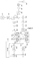
- Fig 1 illustrates a preferred embodiment of a communication signal receiver according to the present invention.
- the preferred embodiment of fig 1 is a homodyne receiver with dual communication channels, which are commonly known as I and Q channels.
- the components of the receiver of fig 1 have been assigned a respective three-digit reference numeral from 100 to 150. All components having a reference numeral, the two rightmost digits of which are identical to the two rightmost digits of a corresponding component in the prior art receiver of fig 4, are identical or have essentially the same function as said corresponding component of fig 4.
- the antenna 100, the bandpass filter 102, the amplifier 104, the splitter 106, the phase shifter 108, the local oscillator 110, the mixers 120 a-b, the lowpass filters 122a-b, the amplifiers 124a-b, the AD converters 126a-b, the digital filters 130a-b, the adders 140a-b and the memory 150 are all identical to, or have essentially the same function as, the antenna 400, bandpass filter 402, amplifier 404, etc. of the generic prior art receiver shown in fig 4.
- the receiver of fig 1 comprises a first average calculator 134a in the first signal path as well as a second average calculator 134b in the second signal path.
- the average calculators 134a-b are arranged to receive, at input nodes 132a-b, the digital samples (as produced by the AD converters 128a-b and filtered by the digital filters 130a-b) and derive an average or mean value of a predetermined number of recently received samples.
- This value which is a time-discrete digital moving average value, is supplied at output nodes 138a-b to the negative terminals of the adders 140a-b, in similarity with the prior art receiver of fig 4.
- the inventive receiver of fig 1 has a feedback loop starting at the respective node 138a-b and ending at a respective first input terminal of a respective data selector or multiplexor 128a-b, which is located between the respective AD converters 126a-b and digital filters 130a-b, as shown in fig 1. Furthermore, a counter 136a-b is connected to the respective average calculator 134a-b. An output of the counter 136a-b is connected to a respective control terminal 129a-b of the selector 128a-b. A second input terminal of the selector 128a-b is connected to the output of the respective AD converter 126a-b.
- the operation of the average calculators 134a-b, the counters 136a-b and the selectors 128a-b is as follows.
- the counter 136a controls the selector 128a, via the control terminal 129a, to forward the stream of digital data symbols received from the AD converter 126a to the digital filter 130a.
- the average calculator 134a continuously calculates an average value of the last n number of digital data symbols, representing the DC level of the digital signal (n is a predetermined number of samples, such as 32-128).
- the counter 136a controls the selector 128a to instead start forwarding the average value calculated by the average calculator 134a to the digital filter 130a.
- the counter 136a maintains the selector 128a in this state, wherein the average value fed back from node 138a is supplied to the digital filter 130a.
- the actual value of the predetermined number of symbol periods depends on the actual implementation of the digital filter 130a. Furthermore, it is common to use not only one digital filter 130a, but a series of digital filters, and the actual number of symbol periods will have to be decided after due consideration and testings. However, for one contemporary GSM receiver, 11 symbol periods have proven to be a suitable number for the time period, during which the digital filter 130a has to be fed with aforesaid average value in order to avoid transient noise in the digital filter.
- the average calculator 134a is arranged to compensate for this DC gain by multiplying with the inverse thereof before supplying its output at node 138a.
- the digital filter 130a is guaranteed to be fed with digital data having a "correct" mean value, i.e. a DC level which is essentially the same as the DC level of the last digital data symbols.
- a "correct" mean value i.e. a DC level which is essentially the same as the DC level of the last digital data symbols.
- transient noise is avoided in the digital filter, since the DC level of the digital signal exhibits no rapid change. Consequently, the receiver circuits prior to the digital filter 130a, e.g. the AD converter 126a, the amplifier 124a, the lowpass filter 122a, the mixer 120a, etc., may be switched to a passive or idle mode immediately after the last wanted data symbol has been sampled. This conserves power as well as facilitates an earlier switch to a transmit mode.
- the above discussion of the operating principle of the components along the first signal path is applicable to the components along the second signal path, i.e. the second average calculator 134b, the second counter 136b, the second selector 128b, etc.
- the first and second counters 136a-b may be combined into a single counter, which is shared between both signal paths.
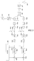
- FIG. 2 An alternative embodiment of the inventive communication signal receiver is shown in fig 2. All components having a reference numeral, the last two digits of which are equal to the last two digits of a corresponding component in the prior art receiver of fig 4, are identical or have essentially the same function.
- the average calculators 239a-b of fig 2 have no means for feeding back a mean value to the digital filters 230a-b; the average calculators 239a-b only have their "normal" function as described above for the prior art receiver of fig 4.
- the embodiment of fig 2 comprises an integrator 234a-b for each signal path.
- the integrator 234a-b is connected to the respective signal path between a selector 228a-b and a digital filter 230a-b.
- the selector 228a-b is identical to or has the same function as the selector 128a-b described with reference to fig 1. Furthermore, the fig 2 embodiment comprises a counter 236a-b having an input connected to the respective integrator 234a-b. An output of the counter 236a-b is connected to a control terminal 229a-b of the respective selector 228a-b.
- the purpose of the integrator 234a-b is to filter out the DC level (i.e. the average value) of the digital signal and to feed back this average value, via an output terminal 238a-b, to the selector 228a-b, once the last wanted digital data symbol has been sampled by the AD converter 226a-b.
- ⁇ is a constant which has to be tuned and set in view of the actual application.
- other FIR or IIR filters with appropriate lowpass characteristics may be used instead of the simple integrator defined by the discrete differential equation above.
- the main operating principle of the embodiment of fig 2 is essentially the same as that of the fig 1 embodiment; an average value representing the DC level of the digital signal is derived and fed back to the digital filter 230a-b for a predetermined number of symbol periods immediately after the last wanted digital data symbol has been sampled, thereby avoiding rapid changes in the DC level of the signal and generation of unwanted transient noise.
- Fig 3 illustrates another alternative embodiment of the present invention.
- all components in fig 3 with a reference numeral, the last two digits of which correspond to the last two digits of a corresponding component in the prior art receiver of fig 4 are identical or have essentially the same function.
- the alternative embodiment of fig 3 solves the problem in the analog domain rather than the digital domain; an integrator comprising a capacitor 334a-b and a selector 328a-b filters out the DC level of the analog signal and stores the result as a voltage across the capacitor 334a-b.
- Controller means not shown in fig 3 is arranged to detect the presence of the last wanted digital data symbol at the AD converter 326a-b and to control the selector 328a-b to switch from a first state, where the selector 328a-b is open and the capacitor 334a-b is disconnected from the first and second signal paths respectively, to a second state, where the selector 328a-b is closed and the capacitor 334a-b is connected to the first and second signal paths, respectively, between the amplifier 324a-b and the AD converter 326a-b.
- the output 338a-b of the respective capacitor 334a-b is supplied to the digital filter 330a-b through the respective AD converter 326a-b, so that the digital filter 330a-b is supplied with a signal with no rapid change in DC level immediately after the last wanted digital symbol has been sampled by the AD converter 326a-b.
- the receiver components prior to the capacitor 334a-b and selector 328a-b, i.e. amplifier 324a-b, lowpass filter 322a-b, etc., may be turned off or switched to a passive/idle mode at the same time.
Landscapes
- Engineering & Computer Science (AREA)
- Power Engineering (AREA)
- Computer Networks & Wireless Communication (AREA)
- Signal Processing (AREA)
- Noise Elimination (AREA)
- Analogue/Digital Conversion (AREA)
- Circuits Of Receivers In General (AREA)
- Burglar Alarm Systems (AREA)
- Dc Digital Transmission (AREA)
- Radio Transmission System (AREA)
- Cable Transmission Systems, Equalization Of Radio And Reduction Of Echo (AREA)
- Input Circuits Of Receivers And Coupling Of Receivers And Audio Equipment (AREA)
- Measuring Pulse, Heart Rate, Blood Pressure Or Blood Flow (AREA)
- Electrophonic Musical Instruments (AREA)
- Radar Systems Or Details Thereof (AREA)
Abstract
Description
- The present invention relates to a communication signal receiver with a plurality of components arranged along at least one signal path, where the components along the or each signal path comprise a filter for processing a received signal and averaging means for deriving a mean value of the signal. The invention also relates to a method of operating a communication signal receiver with a plurality of components arranged along at least one signal path, wherein a received signal is converted to a digital form and the signal is processed by at least one digital filter comprised in said plurality of components.
- Communication signal receivers as set out above are used in e.g. wireless telecommunication devices, such as mobile telephones.
- A generic communication signal receiver according to the prior art is shown in FIG 4. The receiver is a homodyne receiver comprising dual communication channels, which are commonly known as I and Q channels. The dual-channel homodyne receiver of FIG 4 is of a kind, which is frequently used in contemporary digital mobile telephones, such as GSM, DCS or PCS telephones.
- The receiver comprises an
antenna 400 for receiving an incoming electromagnetic communication signal, such as a TDMA signal ("Time Division Multiple Acces") representing a stream of digital data symbols, which have been modulated onto two orthogonal carrier waves. The received signal is fed through abandpass filter 402, amplified in anamplifier 404 and then split into two identical signals in asplitter 406. The first of these signals goes to a first signal path, where it is initially mixed in amixer 420a with an intermediate frequency signal. The intermediate frequency signal is fed from alocal oscillator 410 and passes unmodified through aphase shifter 408. Similarly, the second signal goes to a second signal path, where it is mixed in amixer 420b with the intermediate frequency signal from thelocal oscillator 410, once the phase of the intermediate frequency signal has been shifted by 90° in thephase shifter 408. - The output of the
mixer 420a is filtered by alowpass filter 422a and amplified in asecond amplifier 424a. Subsequently, the signal is fed to anAD converter 426a for sampling the signal and converting it to a digital signal comprising aforesaid stream of data symbols. The digital signal is filtered in adigital lowpass filter 430a, and the digital data symbols contained in the signal are supplied, at anode 432a, to adigital memory 450. Anaverage calculator 439a determines the mean value (DC level) of the digital signal and supplies the mean value to a negative input of anadder 440a. At a positive input the adder receives the digital data symbols, that were previously tapped from the signal path atnode 432a. Thus, theadder 440a will in effect subtract the signal mean value, as determined by theaverage calculator 439a, from the digital signal. - Consequently, the output of the
adder 440a at the end of the first signal path will finally provide a first part of the stream of digital data symbols, that were contained in and carried by the analog signal initially received at theantenna 400. Correspondingly, the second signal path, starting with amixer 420b and ending with anadder 440b, will provide a second part of the stream of digital data. The stream of digital data symbols are subsequently used by other components in the mobile telephone for producing e.g. an audible output through a loudspeaker, such as speech from a party with which the user of the telephone is currently having a telephone conversation. Alternatively, the stream of digital data symbols may represent data messages sent between two computers during a data communication session. - EP-A-0 863 606 discloses a direct conversion receiver comprising mixers for mixing a received signal. A holding circuit is provided for supplying an offset canceling voltage. A switch is controlled by a switch controller for supplying the offset canceling voltage to the output side of the mixers.
- The use of
digital filters 430a-b introduces a delay in the signal path, due to the inherent operational properties of digital filters, such as FIR (Finite Impulse Response) or IIR (Infinite Impulse Response) filters. Ideally, once the last wanted digital data symbol has been sampled, the components prior to the digital filters (such as themixers 420a-b, the amplifiers 404a-b, 424a-b and theAD converters 426a-b) should be switched to a passive or idle mode, in order to preserve power and/or to enter a transmit mode as soon as possible. - However, switching off the receiver circuits immediately after the last wanted data symbol has been sampled causes transient noise from the digital filter, due to the rapid change in the DC level of the signal. Therefore, in order to avoid such generation of noise, it has been necessary for prior art receivers, like the generic one described above, to remain active for a certain period of time after the last wanted data symbol. By doing so, the digital filters are fed with a signal with essentially non-varying DC-level for as long as it takes for the last symbol to pass through the digital filters. Obviously, this contradicts the above objective of allowing an immediate switch to a passive mode or transmit mode.
- Therefore, it is an objective of the present invention to overcome the drawbacks of the prior art approach set out above. In particular, the purpose of the invention is to provide an improved communication signal receiver of the type having a plurality of components arranged along at least one signal path, the components along the or each signal path comprising a filter for processing a received signal and averaging means for deriving a mean value of the signal, where the improvements particularly lie in a more rapid switch from active to passive mode and reduced power consumption.
- These objectives are achieved by connecting an output of the averaging means to a component located prior to the filter along the signal path, so that a mean value (or DC level) of the signal may be selectively fed back to the filter for a period of time immediately following the sampling of the last wanted data symbol. Since the filter will be supplied with a signal with no rapid change in DC level, the receiver circuits may be immediately switched off, after the last wanted data symbol has been sampled, without generating transient noise in the digital filter.
- The objectives are also achieved by a method of operating the communication signal receiver, wherein a received signal is converted to a digital form and the signal is processed by at least one digital filter, by determining an average value of the signal, detecting an event in the signal, and in response thereof feeding the digital filter with the average value.
- Other objectives, advantages and features of the present invention appear from the following detailed description, from the attached patent claims as well as from the drawings.
- Preferred and alternative embodiments of the present invention will now be described in more detail with reference to the accompanying drawings, in which:
- Fig 1 is a schematic block diagram of a preferred embodiment of a communication signal receiver according to the present invention,
- Fig 2 is a schematic block diagram of a first alternative embodiment of the present invention,
- Fig 3 is a schematic block diagram of a second alternative embodiment of the present invention, and
- Fig 4 is a schematic block diagram of a generic communication signal receiver according to the prior art.
- Fig 1 illustrates a preferred embodiment of a communication signal receiver according to the present invention. Much like the prior art receiver of fig 4, the preferred embodiment of fig 1 is a homodyne receiver with dual communication channels, which are commonly known as I and Q channels. The components of the receiver of fig 1 have been assigned a respective three-digit reference numeral from 100 to 150. All components having a reference numeral, the two rightmost digits of which are identical to the two rightmost digits of a corresponding component in the prior art receiver of fig 4, are identical or have essentially the same function as said corresponding component of fig 4. Consequently, the
antenna 100, thebandpass filter 102, theamplifier 104, thesplitter 106, thephase shifter 108, thelocal oscillator 110, the mixers 120 a-b, thelowpass filters 122a-b, theamplifiers 124a-b, theAD converters 126a-b, thedigital filters 130a-b, theadders 140a-b and thememory 150 are all identical to, or have essentially the same function as, theantenna 400,bandpass filter 402,amplifier 404, etc. of the generic prior art receiver shown in fig 4. - Furthermore, the receiver of fig 1 comprises a first
average calculator 134a in the first signal path as well as a secondaverage calculator 134b in the second signal path. Just like theaverage calculators 439a-b in the prior art receiver of fig 4, theaverage calculators 134a-b are arranged to receive, atinput nodes 132a-b, the digital samples (as produced by theAD converters 128a-b and filtered by thedigital filters 130a-b) and derive an average or mean value of a predetermined number of recently received samples. This value, which is a time-discrete digital moving average value, is supplied atoutput nodes 138a-b to the negative terminals of theadders 140a-b, in similarity with the prior art receiver of fig 4. Unlike the prior art receiver, the inventive receiver of fig 1 has a feedback loop starting at therespective node 138a-b and ending at a respective first input terminal of a respective data selector ormultiplexor 128a-b, which is located between therespective AD converters 126a-b anddigital filters 130a-b, as shown in fig 1. Furthermore, acounter 136a-b is connected to the respectiveaverage calculator 134a-b. An output of thecounter 136a-b is connected to arespective control terminal 129a-b of theselector 128a-b. A second input terminal of theselector 128a-b is connected to the output of therespective AD converter 126a-b. - The operation of the
average calculators 134a-b, thecounters 136a-b and theselectors 128a-b is as follows. When the receiver is in a receive mode, i.e. receives and processes a plurality of digital data symbols as described above, thecounter 136a controls theselector 128a, via thecontrol terminal 129a, to forward the stream of digital data symbols received from theAD converter 126a to thedigital filter 130a. Meanwhile, theaverage calculator 134a continuously calculates an average value of the last n number of digital data symbols, representing the DC level of the digital signal (n is a predetermined number of samples, such as 32-128). When it has been established, e.g. by controller means not shown in fig 1, that the last wanted digital data symbol has been sampled by theAD converter 126a, thecounter 136a controls theselector 128a to instead start forwarding the average value calculated by theaverage calculator 134a to thedigital filter 130a. During a predetermined number of symbol periods thecounter 136a maintains theselector 128a in this state, wherein the average value fed back fromnode 138a is supplied to thedigital filter 130a. - As is readily realized by the skilled person, the actual value of the predetermined number of symbol periods depends on the actual implementation of the
digital filter 130a. Furthermore, it is common to use not only onedigital filter 130a, but a series of digital filters, and the actual number of symbol periods will have to be decided after due consideration and testings. However, for one contemporary GSM receiver, 11 symbol periods have proven to be a suitable number for the time period, during which thedigital filter 130a has to be fed with aforesaid average value in order to avoid transient noise in the digital filter. - Since the
digital filter 130a inherently has a certain DC gain, theaverage calculator 134a is arranged to compensate for this DC gain by multiplying with the inverse thereof before supplying its output atnode 138a. - Thanks to the provision of the
average calculator 134a, thecounter 136a and the feedback loop fromnode 138a to theselector 128a, thedigital filter 130a is guaranteed to be fed with digital data having a "correct" mean value, i.e. a DC level which is essentially the same as the DC level of the last digital data symbols. Hence, transient noise is avoided in the digital filter, since the DC level of the digital signal exhibits no rapid change. Consequently, the receiver circuits prior to thedigital filter 130a, e.g. theAD converter 126a, theamplifier 124a, thelowpass filter 122a, themixer 120a, etc., may be switched to a passive or idle mode immediately after the last wanted data symbol has been sampled. This conserves power as well as facilitates an earlier switch to a transmit mode. - The above discussion of the operating principle of the components along the first signal path is applicable to the components along the second signal path, i.e. the second
average calculator 134b, thesecond counter 136b, thesecond selector 128b, etc. As an alternative, since data symbols are received simultaneously and at equal rate on both signal paths, the first andsecond counters 136a-b may be combined into a single counter, which is shared between both signal paths. - An alternative embodiment of the inventive communication signal receiver is shown in fig 2. All components having a reference numeral, the last two digits of which are equal to the last two digits of a corresponding component in the prior art receiver of fig 4, are identical or have essentially the same function. In contrast to fig 1, the
average calculators 239a-b of fig 2 have no means for feeding back a mean value to thedigital filters 230a-b; theaverage calculators 239a-b only have their "normal" function as described above for the prior art receiver of fig 4. Instead, the embodiment of fig 2 comprises anintegrator 234a-b for each signal path. Theintegrator 234a-b is connected to the respective signal path between aselector 228a-b and adigital filter 230a-b. Theselector 228a-b is identical to or has the same function as theselector 128a-b described with reference to fig 1. Furthermore, the fig 2 embodiment comprises a counter 236a-b having an input connected to therespective integrator 234a-b. An output of the counter 236a-b is connected to acontrol terminal 229a-b of therespective selector 228a-b. - The purpose of the
integrator 234a-b is to filter out the DC level (i.e. the average value) of the digital signal and to feed back this average value, via anoutput terminal 238a-b, to theselector 228a-b, once the last wanted digital data symbol has been sampled by theAD converter 226a-b. Theintegrator 234a-b may for instance be implemented as a filter having the following filter equation: y(n)=αy(n-1)+(1-α)x(n), where α is a constant which has to be tuned and set in view of the actual application. However, other FIR or IIR filters with appropriate lowpass characteristics may be used instead of the simple integrator defined by the discrete differential equation above. - Consequently, the main operating principle of the embodiment of fig 2 is essentially the same as that of the fig 1 embodiment; an average value representing the DC level of the digital signal is derived and fed back to the
digital filter 230a-b for a predetermined number of symbol periods immediately after the last wanted digital data symbol has been sampled, thereby avoiding rapid changes in the DC level of the signal and generation of unwanted transient noise. - Fig 3 illustrates another alternative embodiment of the present invention. Just like figs 1 and 2, all components in fig 3 with a reference numeral, the last two digits of which correspond to the last two digits of a corresponding component in the prior art receiver of fig 4, are identical or have essentially the same function. Contrary to the embodiments of figs 1 and 2, the alternative embodiment of fig 3 solves the problem in the analog domain rather than the digital domain; an integrator comprising a
capacitor 334a-b and aselector 328a-b filters out the DC level of the analog signal and stores the result as a voltage across thecapacitor 334a-b. Controller means not shown in fig 3 is arranged to detect the presence of the last wanted digital data symbol at theAD converter 326a-b and to control theselector 328a-b to switch from a first state, where theselector 328a-b is open and thecapacitor 334a-b is disconnected from the first and second signal paths respectively, to a second state, where theselector 328a-b is closed and thecapacitor 334a-b is connected to the first and second signal paths, respectively, between theamplifier 324a-b and theAD converter 326a-b. When theselector 328a-b is in its second state, theoutput 338a-b of therespective capacitor 334a-b is supplied to thedigital filter 330a-b through therespective AD converter 326a-b, so that thedigital filter 330a-b is supplied with a signal with no rapid change in DC level immediately after the last wanted digital symbol has been sampled by theAD converter 326a-b. The receiver components prior to thecapacitor 334a-b andselector 328a-b, i.e. amplifier 324a-b,lowpass filter 322a-b, etc., may be turned off or switched to a passive/idle mode at the same time. - The invention has been described above with reference to preferred and alternative embodiments. This disclosure has exemplifying but not limiting purposes; the scope of the present invention is only limited by the definitions in the appended independent patent claims. In particular, the present invention is equally applicable also to other receiver types not mentioned herein, such as receivers having other than two channels or signal paths and/or employing more than one digital filter per signal path.
Claims (10)
- A communication signal receiver with a plurality of components arranged along at least one signal path, the components along the or each signal path comprising a filter (130a-b, 230a-b) for processing a digitized received signal and averaging means (134a-b, 234a-b) for deriving a mean value of the digitized received signal, wherein an output (138a-b, 238a-b) of the averaging means (134a-b, 234a-b) is connected to a component (128a-b, 228a-b) located prior to the filter (130a-b, 230a-b) along the signal path, said component being operatively connected to the averaging means and the filter and being adapted to receive the digitized received signal, characterized by
a control means (136a-b, 236a-b) operatively connected to said component (128a-b, 228a-b) and being adapted to detect an event in the digitized received signal; wherein
said control means (136a-b, 236a-b) is adapted to control, in response to detecting said event, said component (128a-b, 228a-b) to output to said filter (130a-b, 230a-b) said mean value instead of the digitized received signal. - A communication signal receiver according to claim 1, wherein an input (132a-b) of the averaging means (134a-b) is connected to an output of the filter (130a-b).
- A communication signal receiver according to claim 1, wherein an input of the averaging means (234a-b) is connected to a component (228a-b) located prior to the filter (230a-b) along the signal path.
- A communication signal receiver according to any preceding claim, wherein said component (128a-b, 228a-b) comprises:a selector input operatively connected to the output (138a-b, 238a-b) of the averaging means (134a-b, 234a-b);a selector output operatively connected to an input of the filter (130a-b, 230a-b); anda selector control terminal (129a-b, 229a-b) operatively connected to the control means (136a-b, 236a-b) for controlling whether the digitized received signal received at the selector input is to be supplied at the selector output.
- A communication signal receiver according to any of the previous claims, wherein the control means is a counter (136a-b, 236a-b).
- A communication signal receiver according to any preceding claim, further comprising an AD converter (126a-b, 226a-b) for converting a received analogue signal to the digitized signal.
- A communication signal receiver according to claim 6, wherein said control means (136a-b, 236a-b) is adapted to control said component (128a-b, 228a-b) to output said mean value during a predetermined number of symbol periods immediately after a last wanted digital data symbol has been sampled in the AD converter (126a-b).
- A communication signal receiver according to claim 6 or 7, wherein the averaging means (134a-b, 234a-b) is located after the AD converter (126a-b, 226a-b) along the signal path.
- A method of operating a communication signal receiver with a plurality of components arranged along at least one signal path, comprising, determining an average value of a received signal characterized by the steps of:converting the received signal to a digital signal;feeding the digital signal to at least one digital filter (130a-b, 230a-b) comprised in said plurality of components;processing the digital signal by said at least one digital filter (130a-b, 230a-b);detecting an event in the digital signal; andin response to detecting said event, feeding said at least one digital filter (130a-b, 230a-b) with said average value instead of the digital signal.
- A method according to claim 9, wherein said event is the presence of a certain digital data symbol at a certain component (126a-b, 226a-b) prior to said digital filter (130a-b, 230a-b) along said signal path.
Applications Claiming Priority (3)
| Application Number | Priority Date | Filing Date | Title |
|---|---|---|---|
| SE9804060A SE513332C2 (en) | 1998-11-26 | 1998-11-26 | Communication signal receiver and operating method for the same |
| SE9804060 | 1998-11-26 | ||
| PCT/SE1999/001984 WO2000031884A1 (en) | 1998-11-26 | 1999-11-04 | A communication signal receiver and an operating method therefor |
Publications (2)
| Publication Number | Publication Date |
|---|---|
| EP1131897A1 EP1131897A1 (en) | 2001-09-12 |
| EP1131897B1 true EP1131897B1 (en) | 2006-05-31 |
Family
ID=20413425
Family Applications (1)
| Application Number | Title | Priority Date | Filing Date |
|---|---|---|---|
| EP99972805A Expired - Lifetime EP1131897B1 (en) | 1998-11-26 | 1999-11-04 | Communication signal receivcer and operating method thereof |
Country Status (11)
| Country | Link |
|---|---|
| US (1) | US6608999B1 (en) |
| EP (1) | EP1131897B1 (en) |
| JP (1) | JP4316812B2 (en) |
| CN (1) | CN1145270C (en) |
| AT (1) | ATE328399T1 (en) |
| AU (1) | AU1434100A (en) |
| BR (1) | BR9915713A (en) |
| DE (1) | DE69931654D1 (en) |
| MY (1) | MY124356A (en) |
| SE (1) | SE513332C2 (en) |
| WO (1) | WO2000031884A1 (en) |
Families Citing this family (7)
| Publication number | Priority date | Publication date | Assignee | Title |
|---|---|---|---|---|
| JP4063563B2 (en) * | 2002-03-25 | 2008-03-19 | 株式会社日立国際電気 | Direct detection circuit |
| WO2005048548A2 (en) * | 2003-11-12 | 2005-05-26 | Analog Devices, Inc. | Digital data receiver for edge cellular standard |
| GB2424326B (en) * | 2005-03-18 | 2008-01-16 | Motorola Inc | Receiver for receipt and demodulation of a frequency modulated RF signal and method of operation therein |
| IL180673A0 (en) * | 2007-01-11 | 2007-12-03 | Vadim Leibman | Low power radio frequency receiver |
| JPWO2010046957A1 (en) * | 2008-10-24 | 2012-03-15 | 株式会社アドバンテスト | Quadrature amplitude demodulator, demodulation method, and semiconductor device and test apparatus using them |
| US8781430B2 (en) * | 2009-06-29 | 2014-07-15 | Qualcomm Incorporated | Receiver filtering devices, systems, and methods |
| CN107787553B (en) | 2015-05-20 | 2022-02-11 | 美国亚德诺半导体公司 | System and method for synchronous demodulation |
Family Cites Families (6)
| Publication number | Priority date | Publication date | Assignee | Title |
|---|---|---|---|---|
| US4101839A (en) * | 1974-11-27 | 1978-07-18 | The United States Of America As Represented By The Secretary Of The Navy | Analog-digital ratio detector |
| US4979230A (en) | 1989-12-04 | 1990-12-18 | General Instrument Corporation | Up-conversion homodyne receiver for cable television converter with frequency offset to avoid adjacent channel interference |
| US5838735A (en) * | 1996-07-08 | 1998-11-17 | Telefonaktiebolaget Lm Ericsson | Method and apparatus for compensating for a varying d.c. offset in a sampled signal |
| US5749051A (en) * | 1996-07-18 | 1998-05-05 | Ericsson Inc. | Compensation for second order intermodulation in a homodyne receiver |
| US6175728B1 (en) * | 1997-03-05 | 2001-01-16 | Nec Corporation | Direct conversion receiver capable of canceling DC offset voltages |
| US6081565A (en) * | 1998-02-05 | 2000-06-27 | Lucent Technologies Inc. | Amplitude based coarse automatic gain control circuit |
-
1998
- 1998-11-26 SE SE9804060A patent/SE513332C2/en not_active IP Right Cessation
-
1999
- 1999-11-04 DE DE69931654T patent/DE69931654D1/en not_active Expired - Lifetime
- 1999-11-04 BR BR9915713-6A patent/BR9915713A/en not_active IP Right Cessation
- 1999-11-04 AT AT99972805T patent/ATE328399T1/en not_active IP Right Cessation
- 1999-11-04 CN CNB998158755A patent/CN1145270C/en not_active Expired - Fee Related
- 1999-11-04 EP EP99972805A patent/EP1131897B1/en not_active Expired - Lifetime
- 1999-11-04 JP JP2000584606A patent/JP4316812B2/en not_active Expired - Fee Related
- 1999-11-04 AU AU14341/00A patent/AU1434100A/en not_active Abandoned
- 1999-11-04 WO PCT/SE1999/001984 patent/WO2000031884A1/en not_active Ceased
- 1999-11-19 US US09/443,364 patent/US6608999B1/en not_active Expired - Lifetime
- 1999-11-20 MY MYPI99005076A patent/MY124356A/en unknown
Also Published As
| Publication number | Publication date |
|---|---|
| CN1336039A (en) | 2002-02-13 |
| JP2002530994A (en) | 2002-09-17 |
| EP1131897A1 (en) | 2001-09-12 |
| SE9804060L (en) | 2000-05-27 |
| SE513332C2 (en) | 2000-08-28 |
| BR9915713A (en) | 2001-08-21 |
| SE9804060D0 (en) | 1998-11-26 |
| ATE328399T1 (en) | 2006-06-15 |
| JP4316812B2 (en) | 2009-08-19 |
| CN1145270C (en) | 2004-04-07 |
| DE69931654D1 (en) | 2006-07-06 |
| MY124356A (en) | 2006-06-30 |
| WO2000031884A1 (en) | 2000-06-02 |
| AU1434100A (en) | 2000-06-13 |
| US6608999B1 (en) | 2003-08-19 |
Similar Documents
| Publication | Publication Date | Title |
|---|---|---|
| KR100207966B1 (en) | A variable gain amplifier circuit, an offset control method in a variable gain amplifier circuit, a wireless receiver having a variable gain amplifier circuit, and a wireless receiver method in a wireless receiver having a variable gain amplifier circuit | |
| EP0678974B1 (en) | A transmitter and/or receiver | |
| JP4397443B2 (en) | Image removal transceiver and image removal method | |
| EP1155503B1 (en) | Radio receiver and method for preloading an average dc-offset into a channel filter | |
| JP2007533273A (en) | Dual conversion receiver with programmable intermediate frequency and channel selection | |
| US5444863A (en) | Radio communication apparatus having common circuits usable by transmitter and receiver systems | |
| JP3866290B2 (en) | Method and circuit device for reducing signal offset voltage | |
| KR20060130047A (en) | Multi mode receiver | |
| EP1131897A1 (en) | A communication signal receiver and an operating method therefor | |
| FI114591B (en) | Procedure for realizing a transmitter / receiver and transmitter / receiver | |
| JPH09284162A (en) | Receiver | |
| JP2007527648A (en) | Multiple communication protocol with common sampling rate | |
| EP1573897B1 (en) | Three-phase mixer-systems | |
| JP3369396B2 (en) | Wireless transmission / reception shared frequency converter | |
| KR100339126B1 (en) | Circuit for processing baseband signal | |
| KR100737789B1 (en) | Cordless phone architecture | |
| GB1452254A (en) | Circuit arrangement for a tone pushbutton selection telephone subscriber set | |
| JPH0412056B2 (en) | ||
| KR0183663B1 (en) | Transmission Offset Local Oscillation Signal Control Circuit in Digital Cordless Telephone | |
| KR100506238B1 (en) | Key Phone System and Radio Transmission Method for Radio Broadcast Signal Transmission | |
| JPH11298356A (en) | High frequency signal receiver | |
| JPH10242879A (en) | Community receiver | |
| JPH04362838A (en) | wireless transmission equipment | |
| JPH05129986A (en) | Digital modulator in transmitter-receiver | |
| JPH11330908A (en) | Filter circuit |
Legal Events
| Date | Code | Title | Description |
|---|---|---|---|
| PUAI | Public reference made under article 153(3) epc to a published international application that has entered the european phase |
Free format text: ORIGINAL CODE: 0009012 |
|
| 17P | Request for examination filed |
Effective date: 20010509 |
|
| AK | Designated contracting states |
Kind code of ref document: A1 Designated state(s): AT BE CH CY DE DK ES FI FR GB GR IE IT LI LU MC NL PT SE |
|
| AX | Request for extension of the european patent |
Free format text: AL;LT;LV;MK;RO;SI |
|
| RAP1 | Party data changed (applicant data changed or rights of an application transferred) |
Owner name: TELEFONAKTIEBOLAGET LM ERICSSON (PUBL) |
|
| 17Q | First examination report despatched |
Effective date: 20050304 |
|
| RTI1 | Title (correction) |
Free format text: COMMUNICATION SIGNAL RECEIVER AND OPERATING METHOD THEREOF |
|
| GRAP | Despatch of communication of intention to grant a patent |
Free format text: ORIGINAL CODE: EPIDOSNIGR1 |
|
| RTI1 | Title (correction) |
Free format text: COMMUNICATION SIGNAL RECEIVCER AND OPERATING METHOD THEREOF |
|
| GRAS | Grant fee paid |
Free format text: ORIGINAL CODE: EPIDOSNIGR3 |
|
| GRAA | (expected) grant |
Free format text: ORIGINAL CODE: 0009210 |
|
| AK | Designated contracting states |
Kind code of ref document: B1 Designated state(s): AT BE CH CY DE DK ES FI FR GB GR IE IT LI LU MC NL PT SE |
|
| PG25 | Lapsed in a contracting state [announced via postgrant information from national office to epo] |
Ref country code: NL Free format text: LAPSE BECAUSE OF FAILURE TO SUBMIT A TRANSLATION OF THE DESCRIPTION OR TO PAY THE FEE WITHIN THE PRESCRIBED TIME-LIMIT Effective date: 20060531 Ref country code: LI Free format text: LAPSE BECAUSE OF FAILURE TO SUBMIT A TRANSLATION OF THE DESCRIPTION OR TO PAY THE FEE WITHIN THE PRESCRIBED TIME-LIMIT Effective date: 20060531 Ref country code: IT Free format text: LAPSE BECAUSE OF FAILURE TO SUBMIT A TRANSLATION OF THE DESCRIPTION OR TO PAY THE FEE WITHIN THE PRESCRIBED TIME-LIMIT;WARNING: LAPSES OF ITALIAN PATENTS WITH EFFECTIVE DATE BEFORE 2007 MAY HAVE OCCURRED AT ANY TIME BEFORE 2007. THE CORRECT EFFECTIVE DATE MAY BE DIFFERENT FROM THE ONE RECORDED. Effective date: 20060531 Ref country code: FI Free format text: LAPSE BECAUSE OF FAILURE TO SUBMIT A TRANSLATION OF THE DESCRIPTION OR TO PAY THE FEE WITHIN THE PRESCRIBED TIME-LIMIT Effective date: 20060531 Ref country code: CH Free format text: LAPSE BECAUSE OF FAILURE TO SUBMIT A TRANSLATION OF THE DESCRIPTION OR TO PAY THE FEE WITHIN THE PRESCRIBED TIME-LIMIT Effective date: 20060531 Ref country code: BE Free format text: LAPSE BECAUSE OF FAILURE TO SUBMIT A TRANSLATION OF THE DESCRIPTION OR TO PAY THE FEE WITHIN THE PRESCRIBED TIME-LIMIT Effective date: 20060531 Ref country code: AT Free format text: LAPSE BECAUSE OF FAILURE TO SUBMIT A TRANSLATION OF THE DESCRIPTION OR TO PAY THE FEE WITHIN THE PRESCRIBED TIME-LIMIT Effective date: 20060531 |
|
| REG | Reference to a national code |
Ref country code: GB Ref legal event code: FG4D Ref country code: CH Ref legal event code: EP |
|
| REG | Reference to a national code |
Ref country code: IE Ref legal event code: FG4D |
|
| REF | Corresponds to: |
Ref document number: 69931654 Country of ref document: DE Date of ref document: 20060706 Kind code of ref document: P |
|
| PG25 | Lapsed in a contracting state [announced via postgrant information from national office to epo] |
Ref country code: SE Free format text: LAPSE BECAUSE OF FAILURE TO SUBMIT A TRANSLATION OF THE DESCRIPTION OR TO PAY THE FEE WITHIN THE PRESCRIBED TIME-LIMIT Effective date: 20060831 Ref country code: DK Free format text: LAPSE BECAUSE OF FAILURE TO SUBMIT A TRANSLATION OF THE DESCRIPTION OR TO PAY THE FEE WITHIN THE PRESCRIBED TIME-LIMIT Effective date: 20060831 |
|
| PG25 | Lapsed in a contracting state [announced via postgrant information from national office to epo] |
Ref country code: DE Free format text: LAPSE BECAUSE OF FAILURE TO SUBMIT A TRANSLATION OF THE DESCRIPTION OR TO PAY THE FEE WITHIN THE PRESCRIBED TIME-LIMIT Effective date: 20060901 |
|
| PG25 | Lapsed in a contracting state [announced via postgrant information from national office to epo] |
Ref country code: ES Free format text: LAPSE BECAUSE OF FAILURE TO SUBMIT A TRANSLATION OF THE DESCRIPTION OR TO PAY THE FEE WITHIN THE PRESCRIBED TIME-LIMIT Effective date: 20060911 |
|
| PG25 | Lapsed in a contracting state [announced via postgrant information from national office to epo] |
Ref country code: PT Free format text: LAPSE BECAUSE OF FAILURE TO SUBMIT A TRANSLATION OF THE DESCRIPTION OR TO PAY THE FEE WITHIN THE PRESCRIBED TIME-LIMIT Effective date: 20061031 |
|
| NLV1 | Nl: lapsed or annulled due to failure to fulfill the requirements of art. 29p and 29m of the patents act | ||
| PG25 | Lapsed in a contracting state [announced via postgrant information from national office to epo] |
Ref country code: IE Free format text: LAPSE BECAUSE OF NON-PAYMENT OF DUE FEES Effective date: 20061106 |
|
| PG25 | Lapsed in a contracting state [announced via postgrant information from national office to epo] |
Ref country code: MC Free format text: LAPSE BECAUSE OF NON-PAYMENT OF DUE FEES Effective date: 20061130 |
|
| REG | Reference to a national code |
Ref country code: CH Ref legal event code: PL |
|
| PLBE | No opposition filed within time limit |
Free format text: ORIGINAL CODE: 0009261 |
|
| STAA | Information on the status of an ep patent application or granted ep patent |
Free format text: STATUS: NO OPPOSITION FILED WITHIN TIME LIMIT |
|
| EN | Fr: translation not filed | ||
| 26N | No opposition filed |
Effective date: 20070301 |
|
| PG25 | Lapsed in a contracting state [announced via postgrant information from national office to epo] |
Ref country code: GR Free format text: LAPSE BECAUSE OF FAILURE TO SUBMIT A TRANSLATION OF THE DESCRIPTION OR TO PAY THE FEE WITHIN THE PRESCRIBED TIME-LIMIT Effective date: 20060901 Ref country code: FR Free format text: LAPSE BECAUSE OF FAILURE TO SUBMIT A TRANSLATION OF THE DESCRIPTION OR TO PAY THE FEE WITHIN THE PRESCRIBED TIME-LIMIT Effective date: 20070309 |
|
| PG25 | Lapsed in a contracting state [announced via postgrant information from national office to epo] |
Ref country code: LU Free format text: LAPSE BECAUSE OF NON-PAYMENT OF DUE FEES Effective date: 20061104 |
|
| PG25 | Lapsed in a contracting state [announced via postgrant information from national office to epo] |
Ref country code: FR Free format text: LAPSE BECAUSE OF FAILURE TO SUBMIT A TRANSLATION OF THE DESCRIPTION OR TO PAY THE FEE WITHIN THE PRESCRIBED TIME-LIMIT Effective date: 20060531 Ref country code: CY Free format text: LAPSE BECAUSE OF FAILURE TO SUBMIT A TRANSLATION OF THE DESCRIPTION OR TO PAY THE FEE WITHIN THE PRESCRIBED TIME-LIMIT Effective date: 20060531 |
|
| PGFP | Annual fee paid to national office [announced via postgrant information from national office to epo] |
Ref country code: GB Payment date: 20131127 Year of fee payment: 15 |
|
| GBPC | Gb: european patent ceased through non-payment of renewal fee |
Effective date: 20141104 |
|
| PG25 | Lapsed in a contracting state [announced via postgrant information from national office to epo] |
Ref country code: GB Free format text: LAPSE BECAUSE OF NON-PAYMENT OF DUE FEES Effective date: 20141104 |