EP1131618B1 - Measuring apparatus and method for parallel readout of spr sensors - Google Patents
Measuring apparatus and method for parallel readout of spr sensors Download PDFInfo
- Publication number
- EP1131618B1 EP1131618B1 EP99958102A EP99958102A EP1131618B1 EP 1131618 B1 EP1131618 B1 EP 1131618B1 EP 99958102 A EP99958102 A EP 99958102A EP 99958102 A EP99958102 A EP 99958102A EP 1131618 B1 EP1131618 B1 EP 1131618B1
- Authority
- EP
- European Patent Office
- Prior art keywords
- light
- wavelength
- waveguides
- waveguide array
- waveguide
- Prior art date
- Legal status (The legal status is an assumption and is not a legal conclusion. Google has not performed a legal analysis and makes no representation as to the accuracy of the status listed.)
- Expired - Lifetime
Links
Images


Classifications
-
- G—PHYSICS
- G01—MEASURING; TESTING
- G01N—INVESTIGATING OR ANALYSING MATERIALS BY DETERMINING THEIR CHEMICAL OR PHYSICAL PROPERTIES
- G01N21/00—Investigating or analysing materials by the use of optical means, i.e. using sub-millimetre waves, infrared, visible or ultraviolet light
- G01N21/17—Systems in which incident light is modified in accordance with the properties of the material investigated
- G01N21/25—Colour; Spectral properties, i.e. comparison of effect of material on the light at two or more different wavelengths or wavelength bands
- G01N21/251—Colorimeters; Construction thereof
- G01N21/253—Colorimeters; Construction thereof for batch operation, i.e. multisample apparatus
-
- G—PHYSICS
- G01—MEASURING; TESTING
- G01N—INVESTIGATING OR ANALYSING MATERIALS BY DETERMINING THEIR CHEMICAL OR PHYSICAL PROPERTIES
- G01N21/00—Investigating or analysing materials by the use of optical means, i.e. using sub-millimetre waves, infrared, visible or ultraviolet light
- G01N21/17—Systems in which incident light is modified in accordance with the properties of the material investigated
- G01N21/55—Specular reflectivity
- G01N21/552—Attenuated total reflection
- G01N21/553—Attenuated total reflection and using surface plasmons
Definitions
- the invention relates to a measuring arrangement for the parallel reading of SPR sensors (SPR: surface plasmon resonance).
- the light energy is then converted into charge density waves of the electron gas in the gold layer. These charge density waves are called plasmons.
- plasmons charge density waves
- the receptor or ligand is immobilized on the gold surface. Upon addition of the ligand or receptor, the resonance condition is altered upon attachment of the molecules.
- the simplest arrangement for measuring this effect is a glass prism which is illuminated with a light beam and whose angle of incidence is varied (see, for example, "Biospecific interaction analysis using biosensor technology” Malmqvist, M., Nature 361 (1993) 186-187).
- An improved method is the parallel detection of multiple angles.
- the gold surface is illuminated with a slightly divergent monochromatic beam ( ⁇ 10 ° opening angle) and the reflected light is directed onto a spatially resolving light detector. This creates a clear correlation between the angle of reflection and the position on the detector.
- This construction has the advantage of capturing the angular range of interest without moving components. Therefore, this type of detection will be used in some commercial devices, e.g.
- SPM SPR microscopy
- Optical fibers are also used in WO 98/32002 A1.
- the fiber cable is in one Pipette.
- To realize an array is the. Stringing such Pipettes suggested.
- miniaturization is difficult too realize, especially in the parallel measurement of many different Rehearse.
- DE 196 15 366 A1 discloses a method and a device for simultaneous detection of physical, biological or biochemical Reactions and interactions at or in the surface of samples known. All samples are illuminated simultaneously with light of one wavelength irradiated, and the reflected light is transmitted to a receiver array, e.g. one CCD matrix or a video camera supplied. The samples can matrix-like with the sensor surfaces in a plane on a substrate plate be arranged, in turn, on a transparent support plate which is illuminated. The electrical signals of the Receiver arrays are fed to an evaluation device. After Evaluation of samples with one wavelength, this can be another Value to be set.
- a receiver array e.g. one CCD matrix or a video camera supplied.
- the samples can matrix-like with the sensor surfaces in a plane on a substrate plate be arranged, in turn, on a transparent support plate which is illuminated.
- the electrical signals of the Receiver arrays are fed to an evaluation device. After Evaluation of samples with one wavelength, this can be another Value to be set.
- an SPR measuring element which is planar Waveguide is formed.
- an SPR sensor surface provided on which guided in the waveguide light is reflected.
- the bands each correspond to a small angle of incidence range.
- the invention has for its object to provide a measuring arrangement for simultaneous readout of a plurality of SPR sensors, in particular more as a hundred or a thousand, indicate when the readout process should be completed within a measurement time of less than thirty minutes.
- the array used comprises a Variety of waveguides, taking the term waveguide in the frame the invention is an optical medium to understand in which the light in at least one dimension is guided and the at least two parallel Has interfaces.
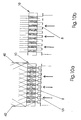
- a planar SPR sensor 1 is used, which can be produced by means of known silicon semiconductor technologies and arranged to form a waveguide array.
- Fig. 1 a part of such a waveguide array is shown.
- a silicon wafer 11 is provided with an SiO 2 layer 12 serving as an optical buffer against the waveguiding layer 13 and the silicon base material 11.
- the waveguide consists of a silicon oxynitride (SiON) layer 13 having a thickness down to about 10 ⁇ m.
- the Siliziumoxynitrid layer 13 is structured by a dry etching process so that parallel strips 14 with widths between 10 .mu.m to 2000 .mu.m and distances between 10 .mu.m and 5000 .mu.m arise.
- the entire wafer is protected by a cover, not shown, except for the areas which are to carry the SPR-capable metal layer 16 in a later process.
- the unprotected in the previous process step vacancies of the waveguide with a metal layer, which is adapted in thickness to the requirements of the SPR measurement, coated.
- the remaining cover of the wafer is removed.
- these recesses can be generated before or after the application of said metal layer.
- the described technology allows multiple parallel arrays of waveguide structures to be accommodated on a wafer. By etching silicon or by sawing the silicon wafer, the multiple parallel arrangements of waveguide structures are singulated.
- the spatial separation of the individual waveguides with one another at the end at which the SPR sensor is located can be realized by wet-chemical etching of the silicon or a sawing process.
- Another variant of the production of waveguides is the ability to produce polymers in thin layers, for example by spin coating onto a substrate.
- the present in dissolved or uncured form of polymers eg PMMA, polycarbonate, UV-curing adhesives or silicon-containing polymers (Cyclotene or ORMOCERE)
- the refractive index of the carrier material must be smaller than that of the polymer to be applied, which later represents the waveguide.
- the SPR waveguide array is brought into contact with the microtiter plate 60 carrying the samples 61 to be characterized for measurements or coating of the SPR-enabled layers 16.
- the SPR waveguide array is introduced into the microtiter plate 60 until the SPR-capable metal regions are completely wetted by the samples 61.
- the individual, vertically arranged waveguides can be arranged in the horizontal at a distance of any microtiter format.
- a waveguide array of the type described is used in a possible first arrangement described below with reference to FIG. 3.
- an IR filter 4 used in the example to protect the optical components and a monochromator 5 only light of a bandwidth of about 0.5 to 5 nm is transmitted.
- the wavelength selection may also be performed with a filter wheel, requiring a corresponding number of filters of similar bandwidth.
- a beam widening optics (L2, L3) then provides a parallel illumination of the entire waveguide array, in the example via a deflection mirror.
- a multi-hole mask 8 provided in the example according to FIG. 3, which can be designed in a variety of ways, shadows the areas behind which there is no waveguide in order to avoid in advance scattered light which could reach any further undesired paths to a detector which is still provided. Is another, more technically complicated way of ordered parallel attachment and fixing a variety of waveguides, eg.
- a nontransparent material or a material provided with a nontransparent coating can be used for the carrier material used, as a result of which the abovementioned multiple-hole mask 8 can be dispensed with.
- the waveguides themselves, with their sensitive area are in a liquid that can be exchanged to make reference measurements in different solutions, to exchange the target molecules, or to do washes.
- the light emerges in the same angle as it was radiated from the other side (see FIG. 6). In the context of the invention is the.
- Light exit-side waveguide sections further associated with a means 9 which causes a scattering of light emerging from the waveguides light.
- a means 9 which causes a scattering of light emerging from the waveguides light.
- This can, for example, by a separately attachable lens, a suitable coating o.ä. be realized.
- the scattering means 9 the light is scattered diffused.
- This strongly divergent light is imaged directly on a CCD chip 20 with the objective L4.
- the objective L4 is designed so that it covers the entire waveguide array, but only a small part of the light emitted from a light guide light can be detected.
- a cooled high-sensitivity CCD camera 20 is used in the example.
- the required exposure time can be up to a few seconds.
- the light emerging from a single waveguide is imaged simultaneously on a plurality of CCD pixels, which leads to an increase in the detection accuracy.
- the image is provided on several camera pixels, because a CCD chip has a much larger number of pixels than the waveguide array provided here on individual waveguides.
- an image processing software is used, which provides an allocation of the range of several CCD pixels to a single waveguide. This is indicated schematically in FIG. 2, for example the pixel region ⁇ (11, 12), (11, 13), ..., (14, 13) ⁇ is assigned to the waveguide 2, 2, ie the region of the CCD chip 20, on which the image of the waveguide 2,2 is made, comprises 12 pixels.
- This assignment is stored in a computer 30 and is maintained throughout the following measurement, because the array is not moved further in the further.
- a fast program algorithm sums over these camera pixel areas, each associated with a waveguide, so that a single intensity value is obtained and stored for each waveguide. Thereafter, the wavelength of the light irradiated from below in the example is shifted by approximately 1 nm with the aid of the monochromator 5 controlled by the computer 30, and the next intensity value is obtained for all the waveguides. This gives a specific intensity spectrum for each waveguide.
- the exposure of the CCD camera is immediately restarted after the data have arrived at the last wavelength in the computer memory and via the control line 31, a new wavelength is set to a controllable by a stepper motor monochromator ,
- the computer summation over the pixel areas can then be made during the exposure time for the new wavelength. If the exposure time is sufficiently long, the calculation time for the summation is negligible. For each wavelength, the time required is essentially given by the exposure time, which in the example is about 5 seconds. For a spectrum of 200 nm, 16 minutes are required.
- a stronger light source 3 such as a Xe arc lamp
- the light first passes through an IR filter 4, a monochromator 5 and a polarizer 6.
- a beam widening optical system L2, L3 then provides parallel illumination of the waveguide array 10, which in this embodiment, however, is spherical. or gradient lenses L5 are upstream.
- several repositioning of the waveguide array 10 with respect to the lenses L5 provided are necessary.
- the parallel light is then focused by the lenses L5 into the gold coated waveguides, for example, such that in the sensitive region of the waveguide the divergent rays strike the intended metal coating of the waveguide at other angles, even at the angle that enables detection of the SPR.
- the lenses L5 provided in the example, approximately one hundred times the light intensity is coupled into the waveguide with respect to the illumination described in FIG.
- the entrance windows 17 of the waveguides are positioned in the example of the focus of the lenses, ie at a distance of a few 100 microns. It is again important to ensure that no light passes the waveguide, such as through any gaps or transparent areas, in the space of the light exit from the waveguides.
- the means described above for example a multiple-hole mask 8.
- the time required can then be reduced to about 1 second due to the stronger light intensity. For example, if you restrict yourself to a spectrum of sixty wavelengths, one minute is needed for all spectra measured in parallel in the example. This makes it possible, for example, to carry out simultaneous kinetic binding studies with a large number of ligands.
- Figs. 10a and 10b The difference between the illumination of the waveguide array 10 with divergent light of Fig. 4 and the parallel light of Fig. 3 will be demonstrated by Figs. 10a and 10b.
- the marginal rays are shown after passing through the multi-hole mask 8 against the background of a sensor line.
- the marginal rays cover a plurality of measurement areas, so that after emergence the marginal ray can no longer be assigned to a single measurement area. Therefore, when illuminated with divergent light, boundary surfaces 40 must be introduced at least at the edge of the sensor area to ensure total reflection , When illuminated with parallel light ( Figure 10b), these interfaces are not needed. The light beam is guided solely by total reflection at the sensor surface and the opposite interface.
- the light beam penetrates the waveguides from the outset at an angle suitable for SPR resonance. If it is now possible to image the entire parallel emerging light on a CCD detector, also an increase in intensity and thus a shortening of the measurement time can be achieved. Here, however, in contrast to FIG. 3, the angle of the incident light is firmly defined.
- FIG. 3 A more elaborate embodiment, which operates according to this principle with a completely parallel beam path and additionally has improved imaging performance (lower edge shading, lower stray-light sensitivity) is shown in FIG.
- the light is guided through an optical fiber 50 via an optical imaging system L1, L1 'to the monochromator 5 and through a further optical fiber 51 to a beam expansion optics L2, L3.
- the illumination of the waveguide array 10 is carried out as described in FIG. 3 with an expanded parallel beam at an angle below which the plasmon resonance is expected.
- a shadow mask (not shown in FIG. 5) may be used. Upon the exit of the light from the sensor, this occurs either offset in parallel (with an even number of reflections, see Fig. 6b) and thus at the angle ⁇ , under which it has entered. With an odd number of reflections ( Figure 6a), it exits at the angle - ⁇ .
- the length L and width B of the SPR-capable waveguide are specially dimensioned in the example of Figure 5 so that the number of reflections is odd and thus the light exits exclusively in the direction of a second deflection mirror 71.
- the parallelism of the exiting light is exploited here to virtually reverse the light path of the illumination:
- the surface of the sensor array 10 to be imaged is not perpendicular to the optical axis of the arrangement, only one line of the object would be sharply imaged in a conventional camera in which the objective is parallel to the CCD chip due to insufficient depth of focus. Therefore, on the image side, the CCD chip 20 must also be tilted to the optical axis, as indicated in Fig. 5, to ensure over the entire sensor array surface 10 a sharp image.
- the CCD camera is adjusted with a goniometer, not shown, with respect to the lens.
- Another advantage of the telescopic imaging is the low stray light sensitivity, because only light that emerges from the object plane at the detection angle is imaged onto the CCD chip.
- FIG. 7 shows a sharp image of a sensor array 10, produced by a beam guide according to FIG. 5.
- the intensity integral is formed over a sensor area.
- an intensity drop resulting from surface plasmon resonance is detected in the spectrum in this way, as shown by way of example in FIG. 8 for a single example.
- the dashed curve in the upper part of Fig. 8 shows the spectrum in which the sensor surface is in air. Essentially, this corresponds to the mathematical folding of lamp spectrum and monochromator transmission.
- the solid line corresponds to the measurement in the presence. from a buffer; This spectrum is superimposed on the surface plasmon resonance.
- the refractive index of the solution is varied by measuring in different sucrose concentrations.
- the upper part of Figure 9 shows how the dip in the spectrum shifts as expected with increasing sucrose concentration.
- An adaptation of the measured data with a Gaussian function provides numerical values for the position of the minima of the spectra.
- a calibration curve can be obtained therefrom, as can be seen in the lower partial image of FIG. 9. For a sufficiently small region of the refractive index, approximately a linear relationship is assumed here.
Landscapes
- Physics & Mathematics (AREA)
- General Physics & Mathematics (AREA)
- Immunology (AREA)
- Life Sciences & Earth Sciences (AREA)
- Chemical & Material Sciences (AREA)
- Analytical Chemistry (AREA)
- Biochemistry (AREA)
- Health & Medical Sciences (AREA)
- Pathology (AREA)
- General Health & Medical Sciences (AREA)
- Spectroscopy & Molecular Physics (AREA)
- Investigating Or Analysing Materials By Optical Means (AREA)
- Sorting Of Articles (AREA)
- Measurement Of Length, Angles, Or The Like Using Electric Or Magnetic Means (AREA)
- Testing Or Calibration Of Command Recording Devices (AREA)
- Arrangements For Transmission Of Measured Signals (AREA)
Abstract
Description
Die Erfindung betrifft eine Meßanordnung zum parallelen Auslesen von SPR-Sensoren (SPR: surface plasmon resonance).The invention relates to a measuring arrangement for the parallel reading of SPR sensors (SPR: surface plasmon resonance).
Auf der Suche nach neuen Wirkstoffen ist die kombinatorische Chemie eine
erfolgversprechende Methode, um die zu einem Rezeptormolekül passenden
Liganden zu finden. Zum Test einer möglichst großen Anzahl von Liganden
ist die Miniaturisierung und die Automatisierung der Syntheseabläufe sowie
deren Parallelisierung eine wichtige Voraussetzung. Aufgrund der dabei
erhaltenen geringen Ligand-Stoffmengen gelten dieselben Anforderungen
(Miniaturisierung, Automatisierung und Parallelisierung) ebenso für den
Nachweis der Ligand-Rezeptorbindung.
Zu diesem Nachweis kann man als sehr empfindliche Methode die
Oberflächenplasmonen Resonanz-Spektroskopie (SPR) benutzen. Dabei wird
das an einer dünnen Goldschicht reflektierte Licht detektiert. Bei geeigneter
Resonanzbedingung (Einfallswinkel und Wellenlänge des Lichtes und
Schichtdicke der Goldschicht) nimmt die Intensität des reflektierten Lichtes
ab. Die Lichtenergie wird dann in Ladungsdichtewellen des Elektronengases
in der Goldschicht umgewandelt. Diese Ladungsdichtewellen nennt man
Plasmonen.
Um die Resonanz zu beobachten, gibt es zwei methodische Ansätze.
Entweder benutzt man monochromatisches Licht und zeichnet die Intensität
des reflektierten Lichtes in Abhängigkeit des Einfallswinkels auf, oder man
hält den Einfallswinkel konstant und variiert die Wellenlänge des Lichtes. In
beiden Fällen wird die Lage der Resonanz verschoben, wenn sich der
Brechungsindex des Mediums ändert, welches sich auf der dem Lichteinfall
abgewandten Seite der Goldschicht befindet.
Diesen Effekt macht man sich bei der biochemischen Analytik zu Nutze. Der
Rezeptor oder Ligand wird auf der Goldoberfläche immobilisiert. Nach der
Zugabe des Liganden oder Rezeptors wird bei Anlagerung der Moleküle die
Resonanzbedingung geändert.
Die einfachste Anordnung zur Messung dieses Effektes ist ein Glasprisma,
das mit einem Lichtstrahl beleuchtet und dessen Einfallswinkel variiert wird
(siehe z.B. "Biospecific interaction analysis using biosensor technology"
Malmqvist, M., Nature 361 (1993) 186-187).
Eine verbesserte Methode ist die parallele Detektion mehrerer Winkel. Dabei
wird die Goldoberfläche mit einem leicht divergenten monochromatischen
Strahl (~10° Öffnungswinkel) beleuchtet und das reflektierte Licht auf einen
ortsauflösenden Lichtdetektor geleitet. Dadurch entsteht eine eindeutige
Zuordnung zwischen dem Reflexionswinkel und der Position auf dem
Detektor. Diese Bauweise hat den Vorteil, ohne bewegliche Bauteile den
interessierenden Winkelbereich zu erfassen. Daher wird diese Art der
Detektion in einigen kommerziellen Geräten, wiez.B. nach WO 90/05295 A1
oder EP 797 091 A1, benutzt. Ein Nachteil dieser Anordnungen besteht
darin, daß jeweils nur ein präpariertes Goldsensorfeld (eindimensionaler
Detektor) oder einige wenige entlang einer Zeile angeordneten Sensorfelder
(mit einem zweidimensionalen Detektor) gleichzeitig untersucht werden
können. Die gleichzeitige Messung einer zweidimensionalen Anordnung von
Sensorflächen ist mit dieser Winkeldetektionsmethode jedoch nicht möglich.
Die thermische Equilibrierung nach dem Einbauen der präparierten
Goldschicht in derartige Geräte dauert jedoch einige Minuten (mindestens
15 min); die eigentliche Messung dauert dann mindestens solange bis die
Molekülanlagerung ins Gleichgewicht gekommen ist, dies kann auch einige
Minuten in Anspruch nehmen. Daher sind solche Geräte nur schlecht für die
Detektion der Bindung von einer großen Anzahl unterschiedlicher Liganden
geeignet, da die Meßzeit und der Aufwand für das Wechseln der Proben
verhältnismäßig groß werden.
Einen parallelen Ansatz zur Analyse eines Probenarrays stellt die SPR-Mikroskopie
(SPM) dar (siehe: EP 388 874 A2 oder M. Zizisperger, W.
Knoll, Progr. Colloid Polym. Sci. 1998, 109, S. 244-253). Hier wird die auf
einem Prisma angebrachte Goldoberfläche an verschiedenen Bereichen mit
verschiedenen Proben belegt und eine Abbildung der Goldoberfläche unter
dem SPR-Winkel auf einen CCD-Chip erzeugt. Während des Meßvorgangs
wird der Winkel mit einer mechanischen Scanvorrichtung geändert. Diese
Methode ist jedoch auf kleine Objektdurchmesser beschränkt.In the search for new drugs, combinatorial chemistry is a promising method for finding the ligand that suits a receptor molecule. To test the largest possible number of ligands, miniaturization and the automation of the synthesis processes and their parallelization is an important prerequisite. Due to the small amounts of ligand thus obtained, the same requirements (miniaturization, automation and parallelization) also apply to the detection of ligand-receptor binding.
For this proof one can use as very sensitive method the surface plasmons resonance spectroscopy (SPR). In this case, the light reflected on a thin gold layer is detected. With a suitable resonance condition (angle of incidence and wavelength of the light and layer thickness of the gold layer), the intensity of the reflected light decreases. The light energy is then converted into charge density waves of the electron gas in the gold layer. These charge density waves are called plasmons.
To observe the resonance, there are two methodological approaches. Either one uses monochromatic light and records the intensity of the reflected light as a function of the angle of incidence, or one keeps the angle of incidence constant and varies the wavelength of the light. In both cases, the position of the resonance is shifted as the refractive index of the medium, which is on the side of the gold layer facing away from the light, changes.
This effect is used in biochemical analysis. The receptor or ligand is immobilized on the gold surface. Upon addition of the ligand or receptor, the resonance condition is altered upon attachment of the molecules.
The simplest arrangement for measuring this effect is a glass prism which is illuminated with a light beam and whose angle of incidence is varied (see, for example, "Biospecific interaction analysis using biosensor technology" Malmqvist, M., Nature 361 (1993) 186-187).
An improved method is the parallel detection of multiple angles. The gold surface is illuminated with a slightly divergent monochromatic beam (~ 10 ° opening angle) and the reflected light is directed onto a spatially resolving light detector. This creates a clear correlation between the angle of reflection and the position on the detector. This construction has the advantage of capturing the angular range of interest without moving components. Therefore, this type of detection will be used in some commercial devices, e.g. according to WO 90/05295 A1 or EP 797 091 A1. A disadvantage of these arrangements is that only one prepared gold sensor array (one-dimensional detector) or a few sensor arrays arranged along a row (with a two-dimensional detector) can be examined simultaneously. The simultaneous measurement of a two-dimensional arrangement of sensor surfaces is not possible with this angle detection method. However, thermal equilibration after incorporation of the prepared gold layer into such devices takes a few minutes (at least 15 minutes); The actual measurement then lasts at least until the molecular attachment has come into equilibrium, this may take several minutes. Therefore, such devices are poorly suited for the detection of the binding of a large number of different ligands, since the measurement time and the cost of changing the samples are relatively large.
A parallel approach for the analysis of a sample array is SPR microscopy (SPM) (see: EP 388 874 A2 or M. Zizisperger, W. Knoll, Progr. Colloid Polym. Sci. 1998, 109, pp. 244-253). Here, the gold surface mounted on a prism is covered with different samples at different areas and an image of the gold surface at the SPR angle is generated on a CCD chip. During the measuring process, the angle is changed with a mechanical scanning device. However, this method is limited to small object diameters.
Eine neuere SPR-Methode wird in WO 94/16312 A1 offenbart. Hier wird die Detektion der Bindung geringer Stoffmengen mittels Lichtleitfasern realisiert, die teilweise mit einer Goldschicht belegt sind. Aber auch hier besteht das Problem in der Konstruktion eines Gerätes, das nach diesem Prinzip viele Proben parallel untersuchen soll. Ein solcher Array von goldbeschichteten Fasern ist einerseits teuer und sehr empfindlich gegen mechanische Verspannungen, andererseits ist die parallele Herstellung des Arrays nach dortigem Vorschlag technisch nur schwer realisierbar.A newer SPR method is disclosed in WO 94/16312 A1. Here is the Detection of the binding of small amounts of substance realized by means of optical fibers, which are partially covered with a gold layer. But even here it is Problem in the design of a device that many according to this principle To examine samples in parallel. Such an array of gold-plated On the one hand, fibers are expensive and very sensitive to mechanical ones Tension, on the other hand, is the parallel production of the array after there technically difficult to implement.
Lichtleitfasern werden auch in WO 98/32002 A1 verwendet. Zum Schutz gegen mechanische Beschädigung befindet sich das Faserkabel in einer Pipette. Zur Realisierung eines Arrays wird das. Aneinanderreihen solcher Pipetten vorgeschlagen. Eine Miniaturisierung ist jedoch schwer zu realisieren, insbesondere bei der parallelen Messung vieler verschiedener Proben.Optical fibers are also used in WO 98/32002 A1. For protection against mechanical damage, the fiber cable is in one Pipette. To realize an array is the. Stringing such Pipettes suggested. However, miniaturization is difficult too realize, especially in the parallel measurement of many different Rehearse.
Aus DE 196 15 366 A1 ist ein Verfahren und eine Einrichtung zum simultanen Nachweis physikalischer, biologischer oder biochemischer Reaktionen und Wechselwirkungen an oder in der Oberfläche von Proben bekannt. Alle Proben werden gleichzeitig mit Licht einer Wellenlänge bestrahlt, und das reflektierte Licht wird einem Empfängerarray, z.B. einer CCD-Matrix oder einer Videokamera zugeführt. Die Proben können matrixartig mit den Sensorflächen in einer Ebene auf einer Substratplatte angeordnet sein, die sich wiederum auf einer transparenten Trägerplatte befindet, welche beleuchtet wird. Die elektrischen Signale des Empfängerarrays werden einer Auswerteeinrichtung zugeführt. Nach der Auswertung der Proben mit einer Wellenlänge, kann diese auf einen anderen Wert eingestellt werden.DE 196 15 366 A1 discloses a method and a device for simultaneous detection of physical, biological or biochemical Reactions and interactions at or in the surface of samples known. All samples are illuminated simultaneously with light of one wavelength irradiated, and the reflected light is transmitted to a receiver array, e.g. one CCD matrix or a video camera supplied. The samples can matrix-like with the sensor surfaces in a plane on a substrate plate be arranged, in turn, on a transparent support plate which is illuminated. The electrical signals of the Receiver arrays are fed to an evaluation device. After Evaluation of samples with one wavelength, this can be another Value to be set.
Aus WO 95/22754 ist eine Analyseeinrichtung bekannt, bei welcher eine Vielzahl von SPR-Analysetrögen matrixförmig angeordnet sind und gleichzeitig ausgemessen werden können. Die Sensorflächen der Analysetröge befinden sich parallel in einer Ebene.From WO 95/22754 an analysis device is known in which a Variety of SPR analysis trays are arranged in a matrix and can be measured at the same time. The sensor surfaces of the Analysis trays are located in parallel in one level.
Aus WO 97/15819 ist ein SPR-Messelement bekannt, das als planarer Wellenleiter ausgebildet ist. Auf einer Seite des Wellenleiters ist eine SPR-Sensorfläche vorgesehen, an welcher in dem Wellenleiter geführtes Licht reflektiert wird. Gemäß dem Messprinzip von WO 97/15819 wird polychromatisches Licht über einen großen Einfallswinkelbereich in eine Endfläche des Wellenleiters eingekoppelt, und am Ausgang entstehen eine Vielzahl von Reflektionsbändem, welche jeweils SPR-Information enthalten. Die Bänder entsprechen jeweils einem kleinen Einfallswinkelbereich.From WO 97/15819 an SPR measuring element is known which is planar Waveguide is formed. On one side of the waveguide is an SPR sensor surface provided on which guided in the waveguide light is reflected. According to the measurement principle of WO 97/15819 Polychromatic light over a large angle of incidence in a End surface of the waveguide coupled, and at the output arise a Plurality of reflection bands each containing SPR information. The bands each correspond to a small angle of incidence range.
Aus US 5,485,277 ist eine SPR-Anordnung bekannt, bei welcher mehrere Sensorflächen, die auf einem Wellenleiter vorgesehen sind, durch den Wellenleiter bestrahlt werden. Das durch SPR modulierte Licht wird mittels eines CCD-Arrays überwacht.From US 5,485,277 an SPR arrangement is known in which several Sensor surfaces, which are provided on a waveguide through the Waveguides are irradiated. The SPR modulated light is using monitored by a CCD array.
Der Erfindung liegt die Aufgabe zugrunde, eine Meßanordnung zum gleichzeitigen Auslesen einer Vielzahl von SPR-Sensoren, insbesondere mehr als einhundert oder tausend, anzugeben, bei der der Auslesevorgang innerhalb einer Meßzeit von weniger als dreißig Minuten beendet sein soll. The invention has for its object to provide a measuring arrangement for simultaneous readout of a plurality of SPR sensors, in particular more as a hundred or a thousand, indicate when the readout process should be completed within a measurement time of less than thirty minutes.
Gelöst wird diese Aufgabe durch die Messanordnung und das Messverfahren der unabhängigen Ansprüche. Vorteilhafte Ausgestaltungen sind Gegenstand der nachgeordneten Ansprüche.This problem is solved by the measuring arrangement and the measuring method the independent claims. Advantageous embodiments are the subject the subordinate claims.
Um die Aufgabe zu lösen, wird ein besonders ausgebildetes Array in einer Anordnung mit bildgebenden Methoden eingesetzt, um ein gleichzeitiges Auslesen zu ermöglichen. Das zum Einsatz gelangende Array umfaßt eine Vielzahl von Wellenleitern, wobei unter dem Begriff Wellenleiter im Rahmen der Erfindung ein optisches Medium zu verstehen ist, in dem das Licht in mindestens einer Dimension geführt wird und das mindestens zwei parallele Grenzflächen besitzt.To solve the problem, a specially trained array in one Arrangement with imaging methods used to create a simultaneous To enable readout. The array used comprises a Variety of waveguides, taking the term waveguide in the frame the invention is an optical medium to understand in which the light in at least one dimension is guided and the at least two parallel Has interfaces.
Die Erfindung soll nachstehend anhand schematischer Ausführungs-beispiele näher erläutert werden. Es zeigen:
- Fig. 1
- eine Ausführungsmöglichkeit eines Teils eines zum Einsatz gelangenden Wellenleiterarrays,
- Fig. 2
- die Zuordnung eines einzelnen SPR-fähigen Sensorelements zu den Pixeln eines CCD-Arrays
- Fig. 3
- eine erste Ausführungsmöglichkeit einer Meßanordnung nach vorliegender Erfindung,
- Fig. 4
- eine Meßanordnung, die nicht unter die Erfindung fällt,
- Fig. 5
- eine weitere Ausführungsmöglichkeit einer Meßanordnung nach vorliegender Erfindung,
- Fig. 6a und b
- zwei verschiedene optische Strahlungsverläufe durch das SPR-fähige Sensorgebiet,
- Fig. 7
- ein CCD-Bild eines SPR-Wellenleiterarrays,
- Fig. 8
- den Intensitätsverlauf eines einzelnen SPR-fähigen Wellenleiters,
- Fig. 9
- die Verschiebung eines Intensitätsverlaufes bei unterschiedlicher Probenkonzentration und
- Fig. 10a und b
- Den Unterschied zwischen der Beleuchtung des Wellenleiterarrays 10 mit divergentem Licht nach einer Ausführungsform gemäß Fig. 4 und parallelem Licht nach Fig. 3 und Fig. 5.
- Fig. 1
- an embodiment of a part of a deployed waveguide array,
- Fig. 2
- the assignment of a single SPR-capable sensor element to the pixels of a CCD array
- Fig. 3
- a first embodiment of a measuring arrangement according to the present invention,
- Fig. 4
- a measuring arrangement, which does not fall under the invention,
- Fig. 5
- a further embodiment of a measuring arrangement according to the present invention,
- Fig. 6a and b
- two different optical radiation paths through the SPR-enabled sensor area,
- Fig. 7
- a CCD image of an SPR waveguide array,
- Fig. 8
- the intensity profile of a single SPR-capable waveguide,
- Fig. 9
- the shift of an intensity profile at different sample concentration and
- Fig. 10a and b
- The difference between the illumination of the
waveguide array 10 with divergent light according to an embodiment according to FIG. 4 and the parallel light according to FIG. 3 and FIG. 5.
Im Rahmen der Erfindung gelangt vorteilhaft ein planarer SPR-Sensor 1 zum
Einsatz, der vermittels bekannter Silizium-Halbleitertechnologien herstellbar
und zu einem Wellenleiterarray angeordnet ist. In Fig. 1 ist ein Teil eines
solchen Wellenleiterarrays dargestellt. Ein Siliziumwafer 11 wird mit einer
SiO2-Schicht 12 versehen, die als optischer Puffer gegenüber der
wellenleitenden Schicht 13 und dem Siliziumbasismaterial 11 dient. Der
Wellenleiter besteht aus einer Siliziumoxynitrid-Schicht (SiON) 13, die eine
Dicke bis herab zu etwa 10 µm aufweist. Die Siliziumoxynitrid-Schicht 13
wird durch einen Trockenätzprozeß so strukturiert, daß parallele Streifen 14
mit Breiten zwischen 10 µm bis 2000 µm und Abständen zwischen 10 µm
und 5000 µm entstehen. Nach der Strukturierung der Wellenleiterstreifen 14
wird der gesamte Wafer durch eine nicht dargestellte Abdeckung bis auf die
Bereiche, die in einem späteren Prozeß die SPR-fähige Metallschicht 16
tragen sollen, geschützt. Anschließend werden die im vorangegangenen
Prozeßschritt ungeschützten freien Stellen des Wellenleiters mit einer
Metallschicht, die in ihrer Dicke den Anforderungen der SPR-Messung
angepaßt ist, beschichtet. Die übrige Abdeckung des Wafers wird entfernt. Je
nach verwendeter Technologie zum Einbringen der kammartigen
Ausnehmungen 15 in den Trägerkörper, können diese Ausnehmungen vor
oder nach dem Aufbringen genannter Metallschicht erzeugt werden.
Die beschriebene Technologie erlaubt, mehrere parallele Anordnungen von
Wellenleiterstrukturen auf einem Wafer unterzubringen. Mittels Ätzen von
Silizium oder durch Zersägen des Siliziumwafers werden die mehrfach
vorhandenen, parallelen Anordnungen von Wellenleiterstrukturen vereinzelt.
Die räumliche Trennung der einzelnen Wellenleiter untereinander an dem
Ende, an dem sich der SPR-Sensor befindet, kann durch naßchemisches Ätzen
des Siliziums oder einen Sägeprozeß realisiert werden. Eine andere Variante
der Herstellung von Wellenleitern besteht in der Möglichkeit, Polymere in
dünnen Schichten z.B. durch Aufschleudern auf ein Substrat herzustellen. Die
in gelöster oder nicht ausgehärteter Form vorliegenden Polymere (z.B.
PMMA, Polycarbonat, UV-härtende Klebstoffe oder siliziumhaltige Polymere
(Cyclotene oder ORMOCERE)) werden auf ein Trägermaterial
aufgeschleudert oder vergossen. Die Brechzahl des Trägermaterials muß
kleiner sein, als die des aufzutragenden Polymers, der später den Wellenleiter
darstellt. Bei Verwendung UV-härtender Polymere erfolgt nach dem
gleichmäßigen Schichtauftrag ein Herauslösen der unbelichteten Bereiche, so
daß schmale parallele Polymer-Streifen auf dem Träger erhalten bleiben. Within the scope of the invention, advantageously a
The described technology allows multiple parallel arrays of waveguide structures to be accommodated on a wafer. By etching silicon or by sawing the silicon wafer, the multiple parallel arrangements of waveguide structures are singulated. The spatial separation of the individual waveguides with one another at the end at which the SPR sensor is located can be realized by wet-chemical etching of the silicon or a sawing process. Another variant of the production of waveguides is the ability to produce polymers in thin layers, for example by spin coating onto a substrate. The present in dissolved or uncured form of polymers (eg PMMA, polycarbonate, UV-curing adhesives or silicon-containing polymers (Cyclotene or ORMOCERE)) are spun on a support material or potted. The refractive index of the carrier material must be smaller than that of the polymer to be applied, which later represents the waveguide. When UV-curing polymers are used, the uneven areas are dissolved out after uniform layer application so that narrow parallel polymer strips are retained on the substrate.
Andere Polymere können durch Prägen oder andere Replikationstechniken in
die Streifenform gebracht werden, wobei das verbleibende Material an den
Stellen, an denen kein Licht geführt werden soll, entsprechend dünn
dimensioniert sein muß. Nach der Strukturierung der Wellenleiterstreifen
wird auch hier der gesamte Wafer durch eine Abdeckung geschützt, bis auf
die Bereiche, die die SPR-fähige Metallschicht tragen sollen. Im nächsten
Schritt werden diese freiliegenden Bereiche mit der SPR-fähigen
Metallschicht 16 beschichtet und im Anschlußdaran werden die abgedeckten,
übrigen Gebiete von der Schutzschicht befreit.
Die beschriebenen Möglichkeiten erlauben es, sehr viele Wellenleiter auf
einem Wafer parallel herzustellen. Nach der Fabrikation der Wellenleiter mit
den SPR-Sensorgebieten werden aus den prozessierten Wafern einzelne
Streifen, bestehend aus vielen parallelen Wellenleitern, durch Trennverfahren,
z. B. Zersägen, präpariert. Durch den Vereinzelungsprozeß entstehen neue
Stirnflächen 17, die so präpariert werden, daß dort eine Ein- oder
Auskopplung von Licht möglich ist.
Mit den beschriebenen Möglichkeiten gelingt es, planar sehr viele SPR-Sensoren
in einer Reihe angeordnet herzustellen. Für die Realisierung eines
Arrays von Sensoren werden mehrere dieser Streifen nach Fig. 1
hintereinander gestapelt angeordnet. Ein solches Array kann nach der
Montage in einem Bereich außerhalb der SPR-fähigen Metallschichten in ein
Polymer eingegossen werden, um dem SPR-Wellenleiterarray zusätzlichen
Halt zu geben. Die Anordnung und der Abstand der einzelnen SPR-fähigen
Sensoren kann entsprechend der Anordnung und des Abstands der Kavitäten
einer vorzulegenden Mikrotiterplatte 60 (siehe Fig. 3) erfolgen. In einem
solchen Fall wird der SPR-Wellenleiterarray für Messungen oder zur
Beschichtung der SPR-fähigen Schichten 16 mit der Mikrotiterplatte 60, die
die zu charakterisierenden Proben 61 trägt, in Kontakt gebracht. Dabei wird
das SPR-Wellenleiterarray soweit in die Mikrotiterplatte 60 eingebracht, bis
die SPR-fähigen Metallbereiche von den Proben 61 vollständig benetzt
werden. Die einzelnen, vertikal angeordneten Wellenleiter sind in der
Horizontalen in einem Abstand eines beliebigen Mikrotiter-Formats
anordenbar.
Ein Wellenleiterarray der beschriebenen Art kommt in einer nachfolgend an
Hand von Fig. 3 beschriebenen möglichen ersten Anordnung zum Einsatz.
Von dem weißen Licht einer Halogenlampe 3 wird nach Durchlaufen einer
geeigneten Strahl-Anpassungsoptik (L1), einem im Beispiel eingesetzten IR
Filter 4 zur Schonung der optischen Bauelemente und einem Monochromator
5 nur Licht einer Bandbreite von etwa 0,5 bis 5 nm transmittiert. Alternativ
kann die Wellenlängenselektion auch mit einem Filterrad durchgeführt
werden, wobei eine entsprechende Anzahl von Filtern mit ähnlicher
Bandbreite erforderlich sind. Danach erfolgt im Beispiel eine Selektion der
Polarisationsrichtung durch einen Polarisator 6 für TM Wellen bezüglich der
SPR-fähigen Schichten 16 der eingesetzten Lichtwellenleiter 13. Eine
Strahlaufweitungsoptik (L2, L3) sorgt dann für eine parallele Beleuchtung des
ganzen Wellenleiterarrays, im Beispiel über einen Umlenkspiegel 7, der so
angebracht ist, daß das Licht in die Wellenleiter 13 unter einem Winkel von
70° bis 90° bezüglich der Normalen der Goldschicht der Wellenleiter einfällt,
denn nur Licht in diesem Winkelbereich kann die Plasmonenresonanz
anregen. Die Verwendung eines Umlenkspiegels dient hier lediglich eines
kompakteren Aufbaus der Meßanordnung. Alternativ könnte auch direkt unter
diesem Winkel eingestrahlt werden. Eine im Beispiel nach Fig. 3 vorgesehene
Mehrfachlochmaske 8, die vielgestaltig ausgeführt sein kann, schattet die
Bereiche ab, hinter denen sich kein Wellenleiter befindet, um Streulicht, das
auf irgendwelchen ungewollten Wegen zu einem weiterhin vorgesehenen
Detektor gelangen könnte, im voraus zu vermeiden. Ist eine andere, technisch
aufwendigere Art der geordneten parallelen Anbringung und Fixierung einer
Vielzahl von Wellenleitern, bspw. von kommerziell verfügbaren mit einem
Kemdurchmesser von ca. 200 µm, vorgesehen, bspw. durch ein Einbetten
einzelner Wellenleiterabschnitte in einen gemeinsamen Träger, was ebenfalls
im Rahmen der Erfindung liegt, so kann für das eingesetzte Trägermaterial
ein nichttransparentes oder ein mit einer nichttransparenten Beschichtung
versehenes Material eingesetzt sein, wodurch die vorstehend genannte
Mehrfachlochmaske 8 entfallen kann. Die Wellenleiter selbst befinden sich
mit ihrem sensitiven Bereich in einer Flüssigkeit, die ausgewechselt werden
kann, um Referenzmessungen in unterschiedlichen Lösungen durchzuführen,
um die Zielmoleküle auszutauschen oder um Waschvorgänge zu tätigen. Am
zum sensitiven Wellenleiterbereich abseitigen Ende der Wellenleiter tritt das
Licht in dem vom Betrag her gleichen Winkel aus, in dem es von der anderen
Seite eingestrahlt wurde (vgl. Fig. 6). Im Rahmen der Erfindung ist den.
lichtaustrittsseitigen Wellenleiterabschnitten weiterhin ein Mittel 9
zugeordnet, das eine Streuung des aus den Wellenleitern austretenden Lichtes
bewirkt. Dies kann bspw. durch eine separat anbringbare Streuscheibe, eine
geeignete Beschichtung o.ä. realisiert sein. Durch dieses streuende Mittel 9
wird das Licht diffus gestreut. Dieses stark divergente Licht wird direkt mit
dem Objektiv L4 auf einen CCD Chip 20 abgebildet. Das Objektiv L4 ist
dabei so auszulegen, daß es das gesamte Wellenleiterarray erfaßt, wobei
jedoch nur ein kleiner Teil des aus einem Lichtleiter emittierten Lichtes
nachgewiesen werden kann. Um diese geringen Lichtmengen zu detektieren,
wird im Beispiel eine gekühlte hochempfindliche CCD-Kamera 20 eingesetzt.
Die dabei erforderliche Belichtungszeit kann bis zu einigen Sekunden
betragen.
Im Rahmen der Erfindung ist vorgesehen, daß das aus einem einzelnen
Wellenleiter austretende Licht auf mehrere CCD-Pixel gleichzeitig abgebildet
wird, was zu einer Steigerung der Nachweisgenauigkeit führt. So ist im
Beispiel die Abbildung auf mehrere Kamerapixel vorgesehen, denn ein
CCD-Chip besitzt eine sehr viel größere Anzahl von Pixeln als das hier
vorgesehene Wellenleiterarray an einzelnen Wellenleitern aufweist. Im
Rahmen der Erfindung wird eine Bildverarbeitungssoftware eingesetzt, die
eine Zuordnung des Bereiches von mehreren CCD Pixeln zu einem einzelnen
Wellenleiter schafft. Dies wird in Fig. 2 schematisch angedeutet, z.B. wird
dem Wellenleiter 2,2 der Pixelbereich {(11,12), (11,13), ..., (14,13)}
zugeordnet, d.h. der Bereich des CCD-Chips 20, auf den die Abbildung des
Wellenleiters 2,2 erfolgt, umfaßt 12 Pixel. Diese Zuordnung wird in einem
Computer 30 abgespeichert und bleibt während der gesamten folgenden
Messung erhalten, denn das Array wird im weiteren nicht mehr bewegt. Ein
schneller Programm-Algorithmus summiert über diese, jeweils einem
Wellenleiter zugeordnete Kamerapixel-Bereiche, so daß zu jedem
Wellenleiter ein einzelner Intensitätswert erhalten und abgespeichert wird.
Danach wird die Wellenlänge des im Beispiel von unten eingestrahlten
Lichtes um ca. 1 nm mit Hilfe des durch den Computer 30 angesteuerten
Monochromators 5 verschoben und der nächste Intensitätswert für alle
Wellenleiter erhalten. Dadurch erhält man für jeden Wellenleiter ein
spezifisches Intensitätsspektrum. Um die Meßzeit zur Aufnahme eines
solchen Spektrums zu optimieren, wird die Belichtung der CCD Kamera
sofort wieder gestartet, nachdem die Daten bei der letzten Wellenlänge im
Computerspeicher angelangt sind und über die Steuerleitung 31 eine neue
Wellenlänge an einem durch einen Schrittmotor ansteuerbaren
Monochromator 5 eingestellt ist. Die Computer-Summation über die
Pixelbereiche kann dann während der Belichtungszeit für die neue
Wellenlänge vorgenommen werden. Bei ausreichend langer Belichtungszeit
ist die Rechenzeit für die Summation vernachlässigbar. Für jede Wellenlänge
ist der Zeitaufwand im wesentlichen durch die Belichtungszeit gegeben, die
im Beispiel etwa 5 Sekunden beträgt. Für ein Spektrum von 200 nm sind
damit 16 Minuten erforderlich. Für eine Bestimmung der am jeweiligen SPR-Sensor
der einzelnen Wellenleiter angelagerten Moleküle ist nun nicht das
absolute Intensitätspektrum einer einzelnen Messung, sondern die Differenz
der Minima der Intensitätsspektren bei einer Messung in reiner Pufferlösung
zu einer zweiten Messung in Anwesenheit des Zielmoleküls notwendig. Erst
diese Wellenlängenverschiebung erlaubt, eine Aussage über die Anlagerung
von Molekülen zu treffen. Die Abfolge von Referenzmessung und
Probenmessung wäre danach innerhalb von 32 min für sämtliche beleuchteten
Wellenleitersensoren möglich.
Eine weitere Anordnung, welche nicht unter die Erfindung fällt,
die die erforderlichen Meßzeiten reduziert, ist in Fig. 4 schematisch
dargestellt. Da der zeitlimitierende Faktor die Belichtungszeit ist, kann durch
größere Lichtmengen in den Wellenleitern die Meßzeit verkürzt werden. Dazu
kann zum einen etwa eine stärkere Lichtquelle 3, wie z.B. eine Xe-Bogenlampe,
eingesetzt werden. Wie in der nach Fg. 3 beschriebenen
Anordnung durchläuft das Licht zunächst einen einen IR-Filter 4, einen
Monochromator 5 und einen Polarisator 6. Eine Strahlaufweitungsoptik L2,
L3 sorgt dann für eine parallele Beleuchtung des Wellenleiterarrays 10, dem
in dieser Ausführungsform jedoch Kugel- oder Gradientenlinsen L5
vorgeordnet sind. Um sämtliche Wellenleiter zu durchleuchten, sind im
dargestellten Beispiel nach Fig. 4 allerdings mehrere Neupositionierungen des
Wellenleiterarrays 10 bezüglich der vorgesehenen Linsen L5 notwendig. Es
liegt jedoch ebenso im Rahmen der Erfindung, jedem Wellenleiter eine
separate Linse zuzuordnen, die bspw. auch baulicher Bestandteil der
betreffenden Mikrotiterplattenböden 62 sein können.
Das parallele Licht wird dann durch die Linsen L5 in die bspw. mit Gold
beschichteten Wellenleiter derart fokussiert, daß im sensitiven Bereich des
Wellenleiters die divergierenden Strahlen die vorgesehene
Metallbeschichtung des Wellenleiters unter anderen Winkeln auch unter dem
Winkel treffen, der den Nachweis der SPR ermöglicht. Mit den im Beispiel
vorgesehenen Linsen L5 wird gegenüber der in Fig. 3 beschriebenen
Beleuchtung etwa die hundertfache Lichtintensität in die Wellenleiter
eingekoppelt. Die Eintrittsfenster 17 der Wellenleiter sind im Beispiel im
Fokus der Linsen positioniert, d.h. in einem Abstand von einigen 100 µm.
Dabei ist wieder darauf zu achten, daß kein Licht am Wellenleiter vorbei,
etwa durch irgendwelche Zwischenräume oder transparente Bereiche, in den
Raum des Lichtaustritts aus den Wellenleitern gelangt. Dies kann auch hier
durch das Vorsehen oben beschriebener Mittel, bspw. einer
Mehrfachlochmaske 8, vermieden werden. Am lichtaustrittsseitigen Ende der
Wellenleiter verläßt das Licht wieder divergent die Lichtwellenleiter und wird
ebenfalls mit Hilfe eines streuenden Mittels 9 und mit einem Objektiv L4 auf
einen CCD-Chip 20 abgebildet.
Die weitere Zuordnung und Auswertung der Lichtintensitäten, die einem
einzelnen Lichtwellenleiter zugeordnet sind, erfolgt wieder, wie zu Fig. 3
beschrieben. Für eine einzelne Wellenlänge kann der Zeitaufwand aufgrund
der stärkeren Lichtintensität dann etwa auf 1 Sekunde reduziert werden.
Beschränkt man sich z.B. auf ein Spektrum von sechzig Wellenlängen,
benötigt man für alle parallel gemessenen Spektren im Beispiel eine Minute.
Damit ist es z.B. möglich, kinetische Bindungsstudien mit einer großen
Anzahl von Liganden gleichzeitig durchzuführen.
Den Unterschied zwischen der Beleuchtung des Wellenleiterarrays 10 mit
divergentem Licht nach Fig. 4 und parallelem
Licht nach Fig. 3 soll durch Fig. 10a und Fig. 10b demonstriert werden. Hier
sind die Randstrahlen nach Durchlaufen der Mehrfachlochmaske 8 vor dem
Hintergrund einer Sensorzeile dargestellt. Im divergenten Fall (Fig. 10a)
überstreichen die Randstrahlen mehrere Meßbereiche, so daß nach Austritt
der Randstrahl nicht mehr einem einzelnen Meßbereich zugeordnet werden
kann: Daher müssen bei Beleuchtung mit divergentem Licht mindestens am
Rand des Sensorgebietes Grenzflächen 40 eingeführt werden, die eine
Totalreflexion gewährleisten. Bei Beleuchtung mit parallelem Licht (Fig. 10b)
werden diese Grenzflächen nicht benötigt. Der Lichtstrahl wird hierbei allein
durch Totalreflexion an der Sensorfläche und der gegenüberliegenden
Grenzfläche geführt. Der Lichtstrahl durchdringt hier die Wellenleiter von
vornherein in einem für die SPR-Resonanz geeigneten Winkel. Wenn es nun
gelingt, das gesamte parallel austretende Licht auf einen CCD Detektor
abzubilden, ist ebenfalls eine Intensitätssteigerung und damit eine Verkürzung
der Meßzeit erreichbar. Hierbei ist jedoch im Gegensatz zu Fig. 3 der Winkel
des eingestrahlten Lichtes fest definiert.
Eine aufwendigere Ausführungsform, die nach diesem Prinzip mit vollständig
parallelem Strahlengang arbeitet und zusätzlich verbesserte
Abbildungsleistungen aufweist (geringere Randabschattung, geringere
Streulichtempfindlichkeit) ist in Fig. 5 dargestellt. Hier wird das Licht durch
eine Lichtleitfaser 50 über ein optisches Abbildungssystem L1, L1' zum
Monochromator 5 und durch eine weitere Lichtleitfaser 51 zu einer
Strahlaufweitungsoptik L2, L3 geführt. Dies hat den Vorteil, daß die
Beleuchtungsstrahlführung unabhängig von der Lichtein- und-auskopplung
am Monochromator 5 justiert werden kann. Die Beleuchtung des
Wellenleiterarrays 10 erfolgt ebenso wie nach Fig. 3 beschrieben mit einem
aufgeweiteten parallelen Strahlenbündel in einem Winkel unter dem die
Plasmonenresonanz erwartet wird. Dabei kann optional wie in Fig. 3 eine in
Fig. 5 nicht dargestellte Lochmaske eingesetzt sein. Beim Austritt des Lichtes
aus dem Sensor tritt dieses entweder parallel versetzt (bei einer geraden
Anzahl von Reflexionen, vgl. Fig. 6b) und somit unter dem Winkel α aus,
unter dem es eingetreten ist. Bei einer ungeraden Anzahl von Reflexionen
(Fig. 6a) tritt es unter dem Winkel -α aus. Die Länge L und Breite B des
SPR-fähigen Wellenleiters sind im Beispiel nach Fig.5 speziell so
dimensioniert, daß die Anzahl der Reflexionen ungerade ist und somit das
Licht ausschließlich in Richtung eines zweiten Umlenkspiegels 71 austritt. Im
Gegensatz zu Fig. 3, bei der mit einer Streuschicht die Abbildung auf eine
CCD Kamera realisiert ist, wird hier die Parallelität des austretenden Lichtes
ausgenutzt um den Lichtweg der Beleuchtung praktisch umzukehren: Über
eine langbrennweitige achromatische Sammellinse L6 (z.B. f=1000 mm) mit
großem Durchmesser und einem geeigneten Objektiv L7 (z.B. f=100 mm)
wird die Fläche des Sensorarrays auf den CCD Chip teleskopartig abgebildet.
Da die abzubildende Oberfläche des Sensorarrays 10 nicht senkrecht zur
optischen Achse der Anordnung steht, würde bei einer herkömmlichen
Kamera, bei der das Objektiv parallel zum CCD-Chip steht, aufgrund nicht
ausreichender Tiefenschärfe nur eine Linie des Objekts scharf abgebildet
werden. Daher muß bildseitig der CCD-Chip 20 ebenfalls zur optischen
Achse verkippt sein, wie in Fig. 5 angedeutet, um über die ganze
Sensorarrayfläche 10 eine scharfe Abbildung zu gewährleisten. Dies kann
dadurch realisiert werden, daß die CCD-Kamera mit einem nicht dargestellten
Goniometer gegenüber dem Objektiv justiert wird.
Ein weiterer Vorteil der teleskopischen Abbildung ist die geringe
Streulichtempfindlichkeit, denn nur Licht, das unter dem Detektionswinkel
aus der Objektebene austritt, wird auf den CCD-Chip abgebildet.
Fig. 7. zeigt eine scharfe Abbildung eines Sensorarrays 10, erzeugt durch eine
Strahlführung gemäß Fig. 5. Für jede Wellenlänge wird ein solches Bild
detektiert und im Computer 30 wird, wie zu Fig. 2 beschrieben, das
Intensitätsintegral über einen Sensorbereich gebildet. Für jeden einzelnen
Sensor wird auf diese Weise ein Intensitätseinbruch, der bei
Oberflächenplasmonenresonanz entsteht, im Spektrum detektiert, wie es in
Fig. 8 für einen einzelnen exemplarisch gezeigt ist. Die gestrichelte Kurve im
oberen Teilbild von Fig. 8 zeigt das Spektrum bei der sich die Sensorfläche an
Luft befindet. Im wesentlichen entspricht dieses der mathematischen Faltung
aus Lampenspektrum und Monochromatortransmission. Die durchgezogene
Linie entspricht der Messung in Gegenwart. von einem Puffer; diesem
Spektrum ist die Oberflächenplasmonenresonanz überlagert. Durch
Normierung auf das Spektrum in Luft wird das reine
Oberflächenresonanzspektrum erhalten, wie es im unteren Teilbild von Fig. 8
dargestellt ist.
Zum Nachweis, daß es sich bei dem detektierten Einbruch im Spektrum um
die Oberflächenplasmonenresonanz handelt, wird der Brechungsindex der
Lösung variiert, indem in verschiedenen Sucrosekonzentrationen gemessen
wird. Das obere Teilbild von Fig. 9 zeigt, wie sich der Einbruch im Spektrum
mit steigender Sucrosekonzentration wie erwartet verschiebt. Eine Anpassung
der Meßdaten mit einer Gauss-Funktion liefert numerische Werte für die Lage
der Minima der Spektren. Mit dem bekannten Brechungsindex der Lösung
kann daraus eine Kalibrierkurve erhalten werden, wie sie im unteren Teilbild
von Fig. 9 zu sehen ist. Für einen ausreichend kleinen Bereich des
Brechungsindexes wird hier näherungsweise ein linearer Zusammenhang
angenommen. Im vorliegenden Beispiel wird eine Verschiebung von 1,4 nm
für eine Brechungsindex-Änderung von 10-3 erhalten. Dabei gelingt es, das
Minimum mit einer Genauigkeit von etwa 0,3 nm zu bestimmen, einem
typischen Wert für eine Resonanzkurve von etwa 50 nm Halbwertsbreite.
Dadurch können Brechungsindexänderungen von 2 · 10-4 nachgewiesen
werden. Dies demonstriert die Sensitivität der Methode bei paralleler
Messung von mehreren hundert oder tausend Proben innerhalb weniger
Minuten. Other polymers may be formed into the strip form by embossing or other replication techniques, with the remaining material being sized correspondingly thin at the locations where no light is to be passed. After structuring the waveguide strips, the entire wafer is also protected by a cover, except for the areas that are to carry the SPR-compatible metal layer. In the next step, these exposed areas are coated with the SPR-
The possibilities described make it possible to produce a large number of waveguides on a wafer in parallel. After fabrication of the waveguides with the SPR sensor regions, individual strips consisting of many parallel waveguides are separated from the processed wafers by means of separation processes, for. As sawing, prepared. The separation process results in new end surfaces 17, which are prepared in such a way that a light input or output is possible there.
With the possibilities described, it is possible to produce a very large number of SPR sensors arranged in a row in a row. For the realization of an array of sensors, several of these strips according to FIG. 1 are stacked one behind the other. Such an array may be cast into a polymer after mounting in an area outside the SPR-capable metal layers to provide additional support to the SPR waveguide array. The arrangement and the spacing of the individual SPR-capable sensors can be carried out according to the arrangement and the spacing of the cavities of a
A waveguide array of the type described is used in a possible first arrangement described below with reference to FIG. 3.
Of the white light of a
In the context of the invention it is provided that the light emerging from a single waveguide is imaged simultaneously on a plurality of CCD pixels, which leads to an increase in the detection accuracy. Thus, in the example, the image is provided on several camera pixels, because a CCD chip has a much larger number of pixels than the waveguide array provided here on individual waveguides. In the context of the invention, an image processing software is used, which provides an allocation of the range of several CCD pixels to a single waveguide. This is indicated schematically in FIG. 2, for example the pixel region {(11, 12), (11, 13), ..., (14, 13)} is assigned to the
Another arrangement, which does not fall under the invention, which reduces the required measurement times is shown schematically in Fig. 4. Since the time-limiting factor is the exposure time, the measurement time can be shortened by larger amounts of light in the waveguides. For this purpose, for example, a stronger
The parallel light is then focused by the lenses L5 into the gold coated waveguides, for example, such that in the sensitive region of the waveguide the divergent rays strike the intended metal coating of the waveguide at other angles, even at the angle that enables detection of the SPR. With the lenses L5 provided in the example, approximately one hundred times the light intensity is coupled into the waveguide with respect to the illumination described in FIG. The
It is again important to ensure that no light passes the waveguide, such as through any gaps or transparent areas, in the space of the light exit from the waveguides. This can also be avoided here by the provision of the means described above, for example a multiple-
The further assignment and evaluation of the light intensities, which are assigned to a single optical waveguide, takes place again, as described for FIG. 3. For a single wavelength, the time required can then be reduced to about 1 second due to the stronger light intensity. For example, if you restrict yourself to a spectrum of sixty wavelengths, one minute is needed for all spectra measured in parallel in the example. This makes it possible, for example, to carry out simultaneous kinetic binding studies with a large number of ligands.
The difference between the illumination of the
A more elaborate embodiment, which operates according to this principle with a completely parallel beam path and additionally has improved imaging performance (lower edge shading, lower stray-light sensitivity) is shown in FIG. Here, the light is guided through an
Another advantage of the telescopic imaging is the low stray light sensitivity, because only light that emerges from the object plane at the detection angle is imaged onto the CCD chip. FIG. 7 shows a sharp image of a
To demonstrate that the detected dip in the spectrum is surface plasmon resonance, the refractive index of the solution is varied by measuring in different sucrose concentrations. The upper part of Figure 9 shows how the dip in the spectrum shifts as expected with increasing sucrose concentration. An adaptation of the measured data with a Gaussian function provides numerical values for the position of the minima of the spectra. With the known refractive index of the solution, a calibration curve can be obtained therefrom, as can be seen in the lower partial image of FIG. 9. For a sufficiently small region of the refractive index, approximately a linear relationship is assumed here. In the present example, a shift of 1.4 nm for a refractive index change of 10 -3 is obtained. It is possible to determine the minimum with an accuracy of about 0.3 nm, a typical value for a resonance curve of about 50 nm half width. As a result, refractive index changes of 2 × 10 -4 can be detected. This demonstrates the sensitivity of the method with parallel measurement of several hundred or a thousand samples within a few minutes.
- 1 -1 -
- planarer SPR-Sensorplanar SPR sensor
- 10 -10 -
- WellenleiterarrayWaveguide array
- 11 -11 -
- Siliziumwafersilicon wafer
- 12 -12 -
- SiO2-SchichtSiO 2 layer
- 13 -13 -
- Lichtwellenleiteroptical fiber
- 14 -14 -
- WellenleiterstreifenFiber strips
- 15 -15 -
- kammartige Ausnehmungencomb-like recesses
- 16 -16 -
- SPR-fähige SchichtSPR-enabled layer
- 17 -17 -
-
Stirnfläche (Eintrittsfenster) des Lichtwellenleiters 13End face (entrance window) of the
optical waveguide 13 - 20 -20 -
- CCD-Chip (Kamera)CCD chip (camera)
- 3 -3 -
- Beleuchtungsquellelighting source
- 4 -4 -
- IR-FilterIR filter
- 5 -5 -
- wellenlängenselektive Baugruppewavelength-selective module
- 6 -6 -
- Polarisatorpolarizer
- 7 -7 -
- Umlenkspiegeldeflecting
- 71 -71 -
- zweiter Umlenkspiegelsecond deflection mirror
- 8 -8th -
- MehrfachlochmaskePerforated mask
- 9 -9 -
- lichtstreuende Mittellight-scattering agents
- 30 -30 -
- Computercomputer
- 31 -31 -
- Steuerleitungcontrol line
- 40 -40 -
- reflektierende Grenzflächenreflective interfaces
- 50, 51-50, 51-
- Lichtleitfaseroptical fiber
- 60 -60 -
- Mikrotiterplattemicrotiter plate
- 61 -61 -
-
Probe in einer Kavität der Mikrotiterplatte 60Sample in a well of the
microtiter plate 60 - 62 -62 -
- Kavitätenbodencavity floor
- B -B -
- Breite des SPR-fähigen WellenleitersWidth of the SPR-capable waveguide
- L -L -
- Länge des SPR-fähigen WellenleitersLength of the SPR-capable waveguide
- α -α -
- Lichtein- und -austrittswinkelLight entry and exit angle
- L1, L1', L2, L3, L4, L6, L7 -L1, L1 ', L2, L3, L4, L6, L7 -
- optische Abbildungssystemeoptical imaging systems
- L5 -L5 -
- Linsenlenses
Claims (22)
- Measuring arrangement for SPR measurements (SPR: surface plasmon resonance), comprising:a waveguide array (10), which comprises a plurality of planar waveguides (13), in which light is guided in at least one dimension via a light entrance side and a light exit side, and which have in each case at least two parallel boundary surfaces, wherein the distances of the individual waveguides (13) correspond to a two-dimensional regular grid and each individual waveguide (13) is provided with an SPR-compatible sensor region (16),an illuminating source (3),a wavelength-selective module (5) and an optical system (L2, L3), which are arranged downstream of the illuminating source (3), wherein the optical system (L2, L3) is designed so that the light entrance sides of the waveguides (13) of the waveguide array (10) are illuminated with parallel light, wherein the wavelength-selective module (5) is designed to set the wavelength of the light to a preset light wavelength,an imaging optical system (L4; L6, L7) and a CCD chip (20), which are. designed so that the light emerging from the light exit sides of the waveguides (13) of the waveguide array (10) is reproduced on the CCD chip, and the light starting from each individual light waveguide (13) is detected by in each case several adjacent CCD pixels of the CCD chip (20), anda computer (30) with image-processing software, which is designed so that a light intensity value of the light starting from each individual light waveguide (13) is calculated, and after data storage of intensity value, set wavelength and coordinate in the waveguide array (10) via a control line (31), adjustment of the wavelength-selective module (5) to a further light wavelength is carried out, for the purpose of recording an intensity spectrum.
- Measuring arrangement according to claim 1, characterised in that a polariser (6) is arranged downstream of the wavelength-selective module (5).
- Measuring arrangement according to claim 1, characterised in that the waveguides (13) are designed like a comb such that the SPR-compatible sensor regions (16) can be introduced into the cavities of a microtitre plate (60).
- Measuring arrangement according to claim 1 or 3, characterised in that light-scattering means (9) are assigned to the light exit-side side of the waveguide array (10).
- Measuring arrangement according to claim 1, 3, or 4, characterised in that masking and/or absorption means are assigned to the light entrance-side side of the waveguide array (10) in order to guarantee that only light emerging from the waveguides reaches the CCD chip (20).
- Measuring arrangement according to claim 5, characterised in that masking means in the form of a multiple-hole mask (8) are assigned to the light entrance-side side of the waveguide array (10).
- Measuring arrangement according to claim 3 or 5, characterised in that the masking and/or absorption means are assigned such that only light entrance into the cavity base regions (62) of a microtitre plate (60) takes place, in which the SPR-compatible sensors are arranged.
- Measuring arrangement according to claim 3 or 5, characterised in that the absorption means assigned to the light entrance-side side of the waveguide array (10) are designed in the form of a microtitre plate, the cavity side walls of which are manufactured from a light-absorbing material.
- Measuring arrangement according to claim 5, characterised in that the absorption means assigned to the light entrance-side side of the waveguide array (10) are designed in the form of a light-absorbing cast which separates the waveguides (13) from one another.
- Measuring arrangement according to claim 1, characterised in that the wavelength-selective module (5) is formed by an incrementally variable monochromator and a deflecting mirror (7) is arranged downstream of the optical imaging system (L2, L3) and guarantees illumination of the light entrance sides of the waveguides (13) with parallel light at a suitable angle.
- Measuring arrangement according to claim 10, characterised in that in addition, a further deflecting mirror (71) is arranged directly downstream of the light exit-side end of the waveguide array (10) and guarantees the reproduction of the waveguide array (10) on a CCD chip (20) at an angle to the optical axis.
- Measuring process for SPR measurements (SPR: surface plasmon resonance), comprising:use of a waveguide array (10), which comprises a plurality of planar waveguides (13), in which light is guided in at least one dimension via a light entrance side and a light exit side, and which have in each case at least two parallel boundary surfaces, wherein the distances of the individual waveguides (13) correspond to a two-dimensional regular grid and each individual waveguide (13) is provided with an SPR-compatible sensor region (16),illuminating the light entrance sides of the waveguides (13) of the waveguide array (10) with parallel light using an illuminating source (3), a wavelength-selective module (5) and an optical system (L2, L3), wherein the wavelength-selective module (5) sets the wavelength of the light to a preset light wavelength,reproducing the light emerging from the light exit sides of the waveguides (13) of the waveguide array (10) on a CCD chip (20) using an imaging optical system (L4; L6, L7), and detecting the light starting from each individual light waveguide (13) by in each case several adjacent CCD pixels of the CCD chip (20), andcalculating a light intensity value of the light starting from each individual light waveguide (13) using a computer (30) with image-processing software, and after data storage of intensity value, set wavelength and coordinate in the waveguide array (10), adjustment of the wavelength-selective module (5) to a further light wavelength, for the purpose of recording an intensity spectrum.
- Measuring process according to claim 12, characterised in that a polariser (6) is arranged downstream of the wavelength-selective module (5).
- Measuring process according to claim 12, characterised in that the waveguides (13) are designed like a comb such that the SPR-compatible sensor regions (16) can be introduced into the cavities of a microtitre plate (60).
- Measuring process according to claim 12 or 14, characterised in that the light at the light exit-side side of the waveguide array (10) is scattered using light-scattering means (9).
- Measuring process according to claim 12, 14, or 15, characterised in that light is masked at the light entrance-side side of the waveguide array (10) using masking and/or absorption means in order to guarantee that only light emerging from the waveguides reaches the CCD chip (20).
- Measuring process according to claim 16, characterised in that masking means in the form of a multiple-hole mask (8) are assigned to the light entrance-side side of the waveguide array (10).
- Measuring process according to claim 14 or 16, characterised in that the masking and/or absorption means are assigned such that only light entrance into the cavity base regions (62) of a microtitre plate (60) takes place, in which the SPR-compatible sensors are arranged.
- Measuring process according to claim 14 or 16, characterised in that the absorption means assigned to the light entrance-side side of the waveguide array (10) are designed in the form of a microtitre plate, the cavity side walls of which are manufactured from a light-absorbing material.
- Measuring process according to claim 16, characterised in that the absorption means assigned to the light entrance-side side of the waveguide array (10) are designed in the form of a light-absorbing cast which separates the waveguides (13) from one another.
- Measuring process according to claim 12, characterised in that the wavelength-selective module (5) is formed by an incrementally variable monochromator and a deflecting mirror (7) is arranged downstream of the optical imaging system (L2, L3) in order to guarantee illumination of the light entrance sides of the waveguides (13) with parallel light at a suitable angle.
- Measuring process according to claim 20, characterised in that in addition, a further deflecting mirror (71) is arranged directly downstream of the light exit-side end of the waveguide array (10) in order to guarantee the reproduction of the waveguide array (10) on a CCD chip (20) at an angle to the optical axis.
Applications Claiming Priority (3)
| Application Number | Priority Date | Filing Date | Title |
|---|---|---|---|
| DE19854370 | 1998-11-20 | ||
| DE19854370 | 1998-11-20 | ||
| PCT/EP1999/008977 WO2000031515A1 (en) | 1998-11-20 | 1999-11-16 | Set-up of measuring instruments for the parallel readout of spr sensors |
Publications (2)
| Publication Number | Publication Date |
|---|---|
| EP1131618A1 EP1131618A1 (en) | 2001-09-12 |
| EP1131618B1 true EP1131618B1 (en) | 2005-10-12 |
Family
ID=7888969
Family Applications (1)
| Application Number | Title | Priority Date | Filing Date |
|---|---|---|---|
| EP99958102A Expired - Lifetime EP1131618B1 (en) | 1998-11-20 | 1999-11-16 | Measuring apparatus and method for parallel readout of spr sensors |
Country Status (10)
| Country | Link |
|---|---|
| US (1) | US6441906B2 (en) |
| EP (1) | EP1131618B1 (en) |
| JP (1) | JP2002530668A (en) |
| AT (1) | ATE306658T1 (en) |
| AU (1) | AU751246B2 (en) |
| CA (1) | CA2351454A1 (en) |
| DE (2) | DE59912658D1 (en) |
| DK (1) | DK1131618T3 (en) |
| ES (1) | ES2251244T3 (en) |
| WO (1) | WO2000031515A1 (en) |
Families Citing this family (28)
| Publication number | Priority date | Publication date | Assignee | Title |
|---|---|---|---|---|
| US6559939B1 (en) * | 1999-10-29 | 2003-05-06 | Avery Dennison Corporation | Method of high throughput haze screening of material |
| DE10008006C2 (en) | 2000-02-22 | 2003-10-16 | Graffinity Pharm Design Gmbh | SPR sensor and SPR sensor arrangement |
| AU4644701A (en) | 2000-02-22 | 2001-09-03 | Graffinity Pharm Design Gmbh | Spr sensor system |
| DE10020313C1 (en) * | 2000-04-20 | 2001-07-05 | Cybio Systems Gmbh | Arrangement for electrochemical analysis in biochemical processes, comprises a light bundle which leaves the acoustically adjustable filter and is simultaneously directed onto the receiving surfaces of several waveguides |
| US6747737B2 (en) * | 2000-06-29 | 2004-06-08 | Carl Zeiss Jena Gmbh | Method for optical detection of an illuminated specimen in a plurality of detection channels |
| DE10055655C2 (en) * | 2000-11-10 | 2003-06-12 | Jandratek Gmbh | Plasmon resonance sensor, in particular for biosensors |
| EP1243916A3 (en) * | 2001-03-22 | 2004-04-14 | Fuji Photo Film Co., Ltd. | Measuring apparatus and measuring chip |
| US6734956B2 (en) * | 2002-05-06 | 2004-05-11 | Reichert, Inc. | Optical configuration and method for differential refractive index measurements |
| JP4109022B2 (en) * | 2002-06-13 | 2008-06-25 | 富士フイルム株式会社 | Measuring device and method of using the measuring device |
| US6804007B2 (en) * | 2002-09-10 | 2004-10-12 | Reichert, Inc. | Apparatus for multiplexing two surface plasma resonance channels onto a single linear scanned array |
| JP4173746B2 (en) * | 2003-02-12 | 2008-10-29 | 富士フイルム株式会社 | measuring device |
| US7057720B2 (en) | 2003-06-24 | 2006-06-06 | Corning Incorporated | Optical interrogation system and method for using same |
| US7292333B2 (en) * | 2003-06-24 | 2007-11-06 | Corning Incorporated | Optical interrogation system and method for 2-D sensor arrays |
| WO2005022131A1 (en) * | 2003-08-27 | 2005-03-10 | Toyo Boseki Kabushiki Kaisha | Surface plasmon resonance device |
| WO2005064317A1 (en) * | 2003-12-26 | 2005-07-14 | Matsushita Electric Industrial Co., Ltd. | Method of analyzing ligand in sample and apparatus for analyzing ligand in sample |
| JP3890362B2 (en) * | 2004-06-17 | 2007-03-07 | 国立大学法人室蘭工業大学 | Surface plasmon resonance phenomenon measuring device |
| WO2006030957A1 (en) * | 2004-09-16 | 2006-03-23 | Canon Kabushiki Kaisha | Device and method for acquiring information on objective substance to be detected by detecting a change of wavelenght characteristics on the optical transmittance |
| US7317519B2 (en) * | 2004-10-29 | 2008-01-08 | Agilent Technologies, Inc. | Swept-angle SPR measurement system |
| CN100520394C (en) * | 2005-03-08 | 2009-07-29 | 中国科学院电子学研究所 | Single-channel multi-parameter surface plasms resonance tester |
| DE102005023489B4 (en) * | 2005-05-17 | 2014-01-30 | Dr. Johannes Heidenhain Gmbh | Position measuring device for determining the position of two along a measuring direction to each other movable objects and method for forming a reference pulse for such a position measuring device |
| US7483127B1 (en) * | 2005-08-08 | 2009-01-27 | Sru Biosystems, Inc. | Method and apparatus for generating an image of biomolecular sensor target area |
| JP2009543055A (en) * | 2006-06-30 | 2009-12-03 | コーニング インコーポレイテッド | Fluid handling system for flow-through assays |
| US8743367B2 (en) * | 2007-05-21 | 2014-06-03 | Bio-Rad Laboratories Inc. | Optical resonance analysis using a multi-angle source of illumination |
| KR100865755B1 (en) * | 2007-06-29 | 2008-10-28 | 삼성전기주식회사 | Multi-channel biosensor using surface plasmon resonance |
| US8530243B2 (en) | 2009-04-20 | 2013-09-10 | Bio-Rad Laboratories Inc. | Non-scanning SPR system |
| US10481089B2 (en) * | 2013-03-12 | 2019-11-19 | Integrated Plasmonics Corporation | Optical detection system with tilted sensor |
| JP7205851B2 (en) * | 2018-05-30 | 2023-01-17 | 国立大学法人東京工業大学 | Refractive index measuring device, refractive index measuring method and program |
| CN112665618B (en) * | 2020-12-17 | 2022-05-17 | 安徽中元新材料技术有限公司 | Morphology-based wavelength sensitive mode extraction device and method |
Citations (2)
| Publication number | Priority date | Publication date | Assignee | Title |
|---|---|---|---|---|
| US5485277A (en) * | 1994-07-26 | 1996-01-16 | Physical Optics Corporation | Surface plasmon resonance sensor and methods for the utilization thereof |
| WO1997015819A1 (en) * | 1995-10-25 | 1997-05-01 | University Of Washington | Surface plasmon resonance light pipe sensor |
Family Cites Families (16)
| Publication number | Priority date | Publication date | Assignee | Title |
|---|---|---|---|---|
| EP0112721B1 (en) * | 1982-12-21 | 1988-05-18 | Ares-Serono N.V. | Assay technique |
| NL8700851A (en) * | 1987-04-10 | 1988-11-01 | Tno | METHOD AND APPARATUS FOR DETECTING VERY LOW CONCENTRATIONS OF A MEASURING MEDIA CHEMICAL COMPONENT USING SURFACE-PLASMON RESONANCE AND ELECTROCHEMICALLY STIMULATED ADSORPTION |
| GB8811919D0 (en) * | 1988-05-20 | 1988-06-22 | Amersham Int Plc | Biological sensors |
| SE462408B (en) * | 1988-11-10 | 1990-06-18 | Pharmacia Ab | OPTICAL BIOSENSOR SYSTEM USING SURFACE MONITORING RESONSE FOR THE DETECTION OF A SPECIFIC BIOMOLIC CYCLE, TO CALIBRATE THE SENSOR DEVICE AND TO CORRECT FOUND BASELINE OPERATION IN THE SYSTEM |
| DE3909144A1 (en) * | 1989-03-21 | 1990-09-27 | Basf Ag | METHOD FOR DETERMINING THE INDEX OF BREAKING AND LAYER THICKNESS LAYERS |
| US5359681A (en) * | 1993-01-11 | 1994-10-25 | University Of Washington | Fiber optic sensor and methods and apparatus relating thereto |
| DE4315211A1 (en) * | 1993-05-07 | 1994-02-03 | Gunnar Brink | Specific molecule detector using near-infrared surface plasmon resonance - has small cover plate of glass, silicon, metal or plastic having same size as precious metal layer carrying specific receptor mols. |
| FI96800C (en) * | 1994-02-16 | 1996-08-26 | Valtion Teknillinen | Device for performing an analysis |
| AT403745B (en) * | 1996-02-29 | 1998-05-25 | Avl Verbrennungskraft Messtech | MEASURING ARRANGEMENT WITH A TRANSPARENT ELEMENT FOR EXCITING AND MEASURING RADIATION |
| JPH1038800A (en) * | 1996-03-19 | 1998-02-13 | Texas Instr Inc <Ti> | Surface plasmon resonance detector with replaceable optical element |
| DE19615366B4 (en) * | 1996-04-19 | 2006-02-09 | Carl Zeiss Jena Gmbh | Method and device for detecting physical, chemical, biological or biochemical reactions and interactions |
| US5917607A (en) * | 1996-04-25 | 1999-06-29 | Fuji Photo Film Co., Ltd. | Surface plasmon sensor for multiple channel analysis |
| AU6134398A (en) * | 1997-01-22 | 1998-08-07 | Biacore Ab | Pipette and carrier assembly for a sensor |
| DE19748211A1 (en) * | 1997-10-31 | 1999-05-06 | Zeiss Carl Fa | Optical array system and reader for microtiter plates |
| DE19814811C1 (en) * | 1998-04-02 | 1999-08-05 | Inst Physikalische Hochtech Ev | Arrangement for surface plasmon resonance spectroscopy |
| DE19923820C2 (en) * | 1998-05-20 | 2001-05-10 | Graffinity Pharm Design Gmbh | SPR sensor for simultaneous detection of a large number of samples in fluid form |
-
1999
- 1999-11-16 EP EP99958102A patent/EP1131618B1/en not_active Expired - Lifetime
- 1999-11-16 AU AU15559/00A patent/AU751246B2/en not_active Ceased
- 1999-11-16 DE DE59912658T patent/DE59912658D1/en not_active Expired - Lifetime
- 1999-11-16 ES ES99958102T patent/ES2251244T3/en not_active Expired - Lifetime
- 1999-11-16 AT AT99958102T patent/ATE306658T1/en not_active IP Right Cessation
- 1999-11-16 JP JP2000584279A patent/JP2002530668A/en active Pending
- 1999-11-16 WO PCT/EP1999/008977 patent/WO2000031515A1/en active IP Right Grant
- 1999-11-16 CA CA002351454A patent/CA2351454A1/en not_active Abandoned
- 1999-11-16 DK DK99958102T patent/DK1131618T3/en active
- 1999-11-16 DE DE19955556A patent/DE19955556B4/en not_active Expired - Fee Related
-
2001
- 2001-05-18 US US09/859,677 patent/US6441906B2/en not_active Expired - Fee Related
Patent Citations (2)
| Publication number | Priority date | Publication date | Assignee | Title |
|---|---|---|---|---|
| US5485277A (en) * | 1994-07-26 | 1996-01-16 | Physical Optics Corporation | Surface plasmon resonance sensor and methods for the utilization thereof |
| WO1997015819A1 (en) * | 1995-10-25 | 1997-05-01 | University Of Washington | Surface plasmon resonance light pipe sensor |
Also Published As
| Publication number | Publication date |
|---|---|
| DK1131618T3 (en) | 2006-02-20 |
| DE59912658D1 (en) | 2005-11-17 |
| US20020001085A1 (en) | 2002-01-03 |
| ATE306658T1 (en) | 2005-10-15 |
| ES2251244T3 (en) | 2006-04-16 |
| EP1131618A1 (en) | 2001-09-12 |
| AU1555900A (en) | 2000-06-13 |
| WO2000031515A1 (en) | 2000-06-02 |
| US6441906B2 (en) | 2002-08-27 |
| CA2351454A1 (en) | 2000-06-02 |
| DE19955556A1 (en) | 2000-06-08 |
| DE19955556B4 (en) | 2004-09-09 |
| AU751246B2 (en) | 2002-08-08 |
| JP2002530668A (en) | 2002-09-17 |
Similar Documents
| Publication | Publication Date | Title |
|---|---|---|
| EP1131618B1 (en) | Measuring apparatus and method for parallel readout of spr sensors | |
| EP1257809B1 (en) | Spr sensor and spr sensor arrangement | |
| EP1259796B1 (en) | Spr sensor system | |
| DE19923820C2 (en) | SPR sensor for simultaneous detection of a large number of samples in fluid form | |
| DE19732619C2 (en) | Optical detector device | |
| EP3428622B1 (en) | Diffractive biosensor | |
| EP1307728B1 (en) | Waveguide grid array and optical measurement arrangement | |
| DE19615366B4 (en) | Method and device for detecting physical, chemical, biological or biochemical reactions and interactions | |
| DE69933193T2 (en) | Integrated optical sensor and method for integrated optical detection of a substance | |
| DE4438391C2 (en) | Device for determining substance-specific parameters of one or fewer molecules by means of correlation spectroscopy | |
| WO1998057151A1 (en) | Device for detecting biochemical or chemical substances by fluorescence excitation and method for its production | |
| EP0469377B1 (en) | Analysis system and method for the determination of an analyte in a liquid sample | |
| EP0618441A2 (en) | Device for lateral-resolved investigation of a lateral heterogen ultra-thin layer | |
| DE2364069A1 (en) | SPECTRAL PHOTOMETER | |
| WO2003056308A1 (en) | Device and method for examining thin layers | |
| DE102010006773A1 (en) | Wavelength-sensitive plasmonically active module for the spectrally resolved detection of light | |
| DE10052165A1 (en) | Surface Plasmon Resonance sensor system has dividers at which radiation is reflected differently to produce contrast between dividers and sensor surfaces | |
| DE69120253T2 (en) | APPARATUS FOR FLUORESCENCE ANALYSIS | |
| DE102018133037B4 (en) | Arrangement and method for detecting optical properties of a sample, in particular for the selective detection of biological molecules and for reading out a molecule occupancy | |
| AT5152U1 (en) | SPR SENSOR SYSTEM |
Legal Events
| Date | Code | Title | Description |
|---|---|---|---|
| PUAI | Public reference made under article 153(3) epc to a published international application that has entered the european phase |
Free format text: ORIGINAL CODE: 0009012 |
|
| 17P | Request for examination filed |
Effective date: 20010605 |
|
| AK | Designated contracting states |
Kind code of ref document: A1 Designated state(s): AT BE CH CY DE DK ES FI FR GB GR IE IT LI LU MC NL PT SE |
|
| AX | Request for extension of the european patent |
Free format text: AL;LT;LV;MK;RO;SI |
|
| 17Q | First examination report despatched |
Effective date: 20021129 |
|
| GRAP | Despatch of communication of intention to grant a patent |
Free format text: ORIGINAL CODE: EPIDOSNIGR1 |
|
| RTI1 | Title (correction) |
Free format text: MEASURING APPARATUS AND METHOD FOR PARALLEL READOUT OF SPR SENSORS |
|
| GRAS | Grant fee paid |
Free format text: ORIGINAL CODE: EPIDOSNIGR3 |
|
| GRAA | (expected) grant |
Free format text: ORIGINAL CODE: 0009210 |
|
| AK | Designated contracting states |
Kind code of ref document: B1 Designated state(s): AT BE CH CY DE DK ES FI FR GB GR IE IT LI LU MC NL PT SE |
|
| PG25 | Lapsed in a contracting state [announced via postgrant information from national office to epo] |
Ref country code: IE Free format text: LAPSE BECAUSE OF FAILURE TO SUBMIT A TRANSLATION OF THE DESCRIPTION OR TO PAY THE FEE WITHIN THE PRESCRIBED TIME-LIMIT Effective date: 20051012 Ref country code: FI Free format text: LAPSE BECAUSE OF FAILURE TO SUBMIT A TRANSLATION OF THE DESCRIPTION OR TO PAY THE FEE WITHIN THE PRESCRIBED TIME-LIMIT Effective date: 20051012 |
|
| REG | Reference to a national code |
Ref country code: GB Ref legal event code: FG4D Free format text: NOT ENGLISH |
|
| REG | Reference to a national code |
Ref country code: CH Ref legal event code: EP |
|
| PGFP | Annual fee paid to national office [announced via postgrant information from national office to epo] |
Ref country code: PT Payment date: 20051021 Year of fee payment: 7 |
|
| GBT | Gb: translation of ep patent filed (gb section 77(6)(a)/1977) |
Effective date: 20051012 |
|
| REG | Reference to a national code |
Ref country code: IE Ref legal event code: FG4D Free format text: LANGUAGE OF EP DOCUMENT: GERMAN |
|
| PGFP | Annual fee paid to national office [announced via postgrant information from national office to epo] |
Ref country code: AT Payment date: 20051114 Year of fee payment: 7 |
|
| PG25 | Lapsed in a contracting state [announced via postgrant information from national office to epo] |
Ref country code: IT Free format text: LAPSE BECAUSE OF NON-PAYMENT OF DUE FEES Effective date: 20051116 Ref country code: CY Free format text: LAPSE BECAUSE OF FAILURE TO SUBMIT A TRANSLATION OF THE DESCRIPTION OR TO PAY THE FEE WITHIN THE PRESCRIBED TIME-LIMIT Effective date: 20051116 |
|
| REF | Corresponds to: |
Ref document number: 59912658 Country of ref document: DE Date of ref document: 20051117 Kind code of ref document: P |
|
| PGFP | Annual fee paid to national office [announced via postgrant information from national office to epo] |
Ref country code: DK Payment date: 20051124 Year of fee payment: 7 |
|
| PGFP | Annual fee paid to national office [announced via postgrant information from national office to epo] |
Ref country code: ES Payment date: 20051128 Year of fee payment: 7 Ref country code: BE Payment date: 20051128 Year of fee payment: 7 |
|
| PG25 | Lapsed in a contracting state [announced via postgrant information from national office to epo] |
Ref country code: MC Free format text: LAPSE BECAUSE OF NON-PAYMENT OF DUE FEES Effective date: 20051130 |
|
| PGFP | Annual fee paid to national office [announced via postgrant information from national office to epo] |
Ref country code: NL Payment date: 20051130 Year of fee payment: 7 |
|
| PGFP | Annual fee paid to national office [announced via postgrant information from national office to epo] |
Ref country code: SE Payment date: 20051202 Year of fee payment: 7 |
|
| PG25 | Lapsed in a contracting state [announced via postgrant information from national office to epo] |
Ref country code: LU Free format text: LAPSE BECAUSE OF NON-PAYMENT OF DUE FEES Effective date: 20051212 |
|
| REG | Reference to a national code |
Ref country code: CH Ref legal event code: NV Representative=s name: NOVAGRAAF INTERNATIONAL SA |
|
| REG | Reference to a national code |
Ref country code: SE Ref legal event code: TRGR |
|
| PG25 | Lapsed in a contracting state [announced via postgrant information from national office to epo] |
Ref country code: GR Free format text: LAPSE BECAUSE OF FAILURE TO SUBMIT A TRANSLATION OF THE DESCRIPTION OR TO PAY THE FEE WITHIN THE PRESCRIBED TIME-LIMIT Effective date: 20060112 |
|
| REG | Reference to a national code |
Ref country code: DK Ref legal event code: T3 |
|
| REG | Reference to a national code |
Ref country code: ES Ref legal event code: FG2A Ref document number: 2251244 Country of ref document: ES Kind code of ref document: T3 |
|
| REG | Reference to a national code |
Ref country code: IE Ref legal event code: FD4D |
|
| ET | Fr: translation filed | ||
| PLBE | No opposition filed within time limit |
Free format text: ORIGINAL CODE: 0009261 |
|
| STAA | Information on the status of an ep patent application or granted ep patent |
Free format text: STATUS: NO OPPOSITION FILED WITHIN TIME LIMIT |
|
| 26N | No opposition filed |
Effective date: 20060713 |
|
| PG25 | Lapsed in a contracting state [announced via postgrant information from national office to epo] |
Ref country code: AT Free format text: LAPSE BECAUSE OF NON-PAYMENT OF DUE FEES Effective date: 20061116 |
|
| PG25 | Lapsed in a contracting state [announced via postgrant information from national office to epo] |
Ref country code: SE Free format text: LAPSE BECAUSE OF NON-PAYMENT OF DUE FEES Effective date: 20061117 |
|
| PG25 | Lapsed in a contracting state [announced via postgrant information from national office to epo] |
Ref country code: DK Free format text: LAPSE BECAUSE OF NON-PAYMENT OF DUE FEES Effective date: 20061130 Ref country code: BE Free format text: LAPSE BECAUSE OF NON-PAYMENT OF DUE FEES Effective date: 20061130 |
|
| PG25 | Lapsed in a contracting state [announced via postgrant information from national office to epo] |
Ref country code: PT Free format text: LAPSE BECAUSE OF NON-PAYMENT OF DUE FEES Effective date: 20070516 |
|
| REG | Reference to a national code |
Ref country code: PT Ref legal event code: MM4A Free format text: LAPSE DUE TO NON-PAYMENT OF FEES Effective date: 20070516 |
|
| PG25 | Lapsed in a contracting state [announced via postgrant information from national office to epo] |
Ref country code: NL Free format text: LAPSE BECAUSE OF NON-PAYMENT OF DUE FEES Effective date: 20070601 |
|
| REG | Reference to a national code |
Ref country code: DK Ref legal event code: EBP |
|
| EUG | Se: european patent has lapsed | ||
| NLV4 | Nl: lapsed or anulled due to non-payment of the annual fee |
Effective date: 20070601 |
|
| BERE | Be: lapsed |
Owner name: *GRAFFINITY PHARMACEUTICAL DESIGN G.M.B.H. Effective date: 20061130 |
|
| REG | Reference to a national code |
Ref country code: ES Ref legal event code: FD2A Effective date: 20061117 |
|
| PG25 | Lapsed in a contracting state [announced via postgrant information from national office to epo] |
Ref country code: ES Free format text: LAPSE BECAUSE OF NON-PAYMENT OF DUE FEES Effective date: 20061117 |
|
| PGFP | Annual fee paid to national office [announced via postgrant information from national office to epo] |
Ref country code: GB Payment date: 20101020 Year of fee payment: 12 |
|
| REG | Reference to a national code |
Ref country code: CH Ref legal event code: PFA Owner name: GRAFFINITY PHARMACEUTICAL DESIGN GMBH Free format text: GRAFFINITY PHARMACEUTICAL DESIGN GMBH#IM NEUENHEIMER FELD 515#69120 HEIDELBERG (DE) -TRANSFER TO- GRAFFINITY PHARMACEUTICAL DESIGN GMBH#IM NEUENHEIMER FELD 515#69120 HEIDELBERG (DE) |
|
| PGFP | Annual fee paid to national office [announced via postgrant information from national office to epo] |
Ref country code: CH Payment date: 20111031 Year of fee payment: 13 Ref country code: FR Payment date: 20111201 Year of fee payment: 13 |
|
| REG | Reference to a national code |
Ref country code: CH Ref legal event code: PL |
|
| GBPC | Gb: european patent ceased through non-payment of renewal fee |
Effective date: 20121116 |
|
| PG25 | Lapsed in a contracting state [announced via postgrant information from national office to epo] |
Ref country code: CH Free format text: LAPSE BECAUSE OF NON-PAYMENT OF DUE FEES Effective date: 20121130 Ref country code: LI Free format text: LAPSE BECAUSE OF NON-PAYMENT OF DUE FEES Effective date: 20121130 |
|
| REG | Reference to a national code |
Ref country code: FR Ref legal event code: ST Effective date: 20130731 |
|
| PG25 | Lapsed in a contracting state [announced via postgrant information from national office to epo] |
Ref country code: GB Free format text: LAPSE BECAUSE OF NON-PAYMENT OF DUE FEES Effective date: 20121116 Ref country code: FR Free format text: LAPSE BECAUSE OF NON-PAYMENT OF DUE FEES Effective date: 20121130 |
|
| PGFP | Annual fee paid to national office [announced via postgrant information from national office to epo] |
Ref country code: DE Payment date: 20131120 Year of fee payment: 15 |
|
| REG | Reference to a national code |
Ref country code: DE Ref legal event code: R119 Ref document number: 59912658 Country of ref document: DE |
|
| PG25 | Lapsed in a contracting state [announced via postgrant information from national office to epo] |
Ref country code: DE Free format text: LAPSE BECAUSE OF NON-PAYMENT OF DUE FEES Effective date: 20150602 |