EP1130777B1 - Solid state relay - Google Patents
Solid state relay Download PDFInfo
- Publication number
- EP1130777B1 EP1130777B1 EP01301790A EP01301790A EP1130777B1 EP 1130777 B1 EP1130777 B1 EP 1130777B1 EP 01301790 A EP01301790 A EP 01301790A EP 01301790 A EP01301790 A EP 01301790A EP 1130777 B1 EP1130777 B1 EP 1130777B1
- Authority
- EP
- European Patent Office
- Prior art keywords
- switch
- solid state
- state relay
- primary
- coupling
- Prior art date
- Legal status (The legal status is an assumption and is not a legal conclusion. Google has not performed a legal analysis and makes no representation as to the accuracy of the status listed.)
- Expired - Lifetime
Links
- 239000007787 solid Substances 0.000 title claims abstract description 27
- 230000003287 optical effect Effects 0.000 claims abstract description 13
- 238000013459 approach Methods 0.000 claims abstract description 4
- 238000010168 coupling process Methods 0.000 claims description 30
- 238000005859 coupling reaction Methods 0.000 claims description 30
- 230000008878 coupling Effects 0.000 claims description 25
- 230000005669 field effect Effects 0.000 claims description 7
- 229910044991 metal oxide Inorganic materials 0.000 claims description 2
- 150000004706 metal oxides Chemical class 0.000 claims description 2
- 230000004044 response Effects 0.000 claims description 2
- 239000004065 semiconductor Substances 0.000 claims description 2
- 239000011324 bead Substances 0.000 description 9
- 229910000859 α-Fe Inorganic materials 0.000 description 9
- 229910052732 germanium Inorganic materials 0.000 description 3
- GNPVGFCGXDBREM-UHFFFAOYSA-N germanium atom Chemical compound [Ge] GNPVGFCGXDBREM-UHFFFAOYSA-N 0.000 description 3
- XUIMIQQOPSSXEZ-UHFFFAOYSA-N Silicon Chemical compound [Si] XUIMIQQOPSSXEZ-UHFFFAOYSA-N 0.000 description 2
- 238000012986 modification Methods 0.000 description 2
- 230000004048 modification Effects 0.000 description 2
- 229910052710 silicon Inorganic materials 0.000 description 2
- 239000010703 silicon Substances 0.000 description 2
- 230000009471 action Effects 0.000 description 1
- 238000001514 detection method Methods 0.000 description 1
- 238000010304 firing Methods 0.000 description 1
- 230000009467 reduction Effects 0.000 description 1
- 230000000717 retained effect Effects 0.000 description 1
- 238000001228 spectrum Methods 0.000 description 1
- 230000001960 triggered effect Effects 0.000 description 1
Images




Classifications
-
- H—ELECTRICITY
- H03—ELECTRONIC CIRCUITRY
- H03K—PULSE TECHNIQUE
- H03K17/00—Electronic switching or gating, i.e. not by contact-making and –breaking
- H03K17/16—Modifications for eliminating interference voltages or currents
-
- H—ELECTRICITY
- H03—ELECTRONIC CIRCUITRY
- H03K—PULSE TECHNIQUE
- H03K17/00—Electronic switching or gating, i.e. not by contact-making and –breaking
- H03K17/13—Modifications for switching at zero crossing
- H03K17/136—Modifications for switching at zero crossing in thyristor switches
-
- H—ELECTRICITY
- H03—ELECTRONIC CIRCUITRY
- H03K—PULSE TECHNIQUE
- H03K17/00—Electronic switching or gating, i.e. not by contact-making and –breaking
- H03K17/51—Electronic switching or gating, i.e. not by contact-making and –breaking characterised by the components used
- H03K17/78—Electronic switching or gating, i.e. not by contact-making and –breaking characterised by the components used using opto-electronic devices, i.e. light-emitting and photoelectric devices electrically- or optically-coupled
- H03K17/79—Electronic switching or gating, i.e. not by contact-making and –breaking characterised by the components used using opto-electronic devices, i.e. light-emitting and photoelectric devices electrically- or optically-coupled controlling bipolar semiconductor switches with more than two PN-junctions, or more than three electrodes, or more than one electrode connected to the same conductivity region
Definitions
- the present invention as it is defined is the independent claim relates to solid state relay circuits.
- a relay In general, a relay is an electrical switching device in which operation of the switch is controlled by an electrical control signal applied to the relay.
- Conventional relays are electromechanical devices.
- a solid state relay (SSR) on the other hand, is comprised entirely of solid state components and, unlike electromagnetic relays, involves no mechanical movement to provide the required switching operation.
- An example of solid state relay is disclosed in the document GB-A-2 062 372 .
- SSRs are commonly used to provide a safe interface between low voltage control circuits and high voltage, high current electrical equipment. Because it has no moving parts and is sealed, the SSR has become an essential component in a wide range of electrical equipment.
- the design of conventional SSRs suffers a serious disadvantage because it switches alternating current (AC) at random points in the sinusoidal waveform, causing bursts of electrical noise to be generated.
- AC alternating current
- Improved designs seek to operate the switch at zero volts in the waveform, but there is still an uncertainty of at least +/- 1.8 volts in the switching voltage, which still produces considerable noise.
- One widely-used SSR design consists of a reversed, back-to-back pair of thyristors triggered by a crude, zero volts sensing device and can normally only be switched on when the voltage across the thyristors is greater than approximately 2V.
- the energy released by the switching action distorts the AC power waveform, typically by at least 2% at 100V.
- Such devices also switch on with a steep rise, increasing the harmonic content of the noise generated and so increasing the width of the frequency spectrum affected.
- a solid state relay comprising:
- said primary switching means comprises a pair of inverse back-to-back thyristors.
- a pair of inverse back-to-back alternistors may be used.
- a pair of inverse back-to-back triacs may be used.
- the second coupling means may be magnetic coupling, electrostatic coupling or piezoelectric coupling.
- said light emitting means comprise Light Emitting Diodes (LEDs).
- LEDs Light Emitting Diodes
- said optical switch comprises a photo-transistor.
- said second coupling means is an opto-coupling means
- said second signal emitting means is a light emitting means
- said signal receiving means is a photosensitive means
- said photo-sensitive means comprises a photovoltaic cell.
- said pilot switch means comprises a thyristor.
- the switch circuit includes secondary switch means responsive to said photo-sensitive means and adapted to trigger said primary switch means and to conduct said AC power supply in parallel with said primary switching means during a time interval between the switching on of said pilot switch and the AC power supply voltage amplitude reaching a predetermined minimum value at which the primary switch means takes over full conduction of the AC power supply.
- said secondary switch means comprises a pair of gate-source coupled Field Effect Transistors (FETs) having their respective drains connected to the gates of the thyristor means of the primary switch means and first and second diode means connected between the gates of said thyristor means and AC supply terminals of the switch circuit.
- FETs field Effect Transistors
- the operation of said FETs is controlled by said photo-sensitive means.
- said FETs are power Metal Oxide Semiconductor Field Effect Transistors.
- said diode means comprise Schottky diodes.
- said diode means comprise transistors, the operation of which is controlled by further optical coupling means each comprising light emitting means in the control circuit, the operation of which is controlled by said pilot switch means, and photo-sensitive means (preferably a photovoltaic cell) in the switch circuit.
- a solid state relay with means for sensing a zero volts crossing point in a waveform
- said solid state relay including primary switching means and secondary switching means
- said secondary switching means is adapted to trigger said primary switching means and to conduct an AC power supply in parallel with said primary switching means during a time interval between the switching on of a pilot switch and the AC power supply voltage amplitude reaching a predetermined minimum value at which the primary switch means takes over full conduction of the AC power supply.
- said secondary switch means comprises a pair of gate-source coupled Field Effect Transistors (FETs) having their respective drains connected to the gates of the thyristor means of the primary switch means and first and second diode means connected between the gates of said thyristor means and AC supply terminals of the switch circuit.
- FETs field Effect Transistors
- Fig. 1 shows a SSR circuit 1, comprising a switch circuit 2 and a control circuit 4.
- the circuits 2 and 4 are electrically isolated from one another, being coupled by first and second opto-coupling means 11/12 and 19/26.
- the switch circuit 2 includes switching means comprising an inverse back-to-back pair of thyristors 7 and 9, connected in parallel between an AC input terminal 3 and an AC output terminal 5, so that operation of the thyristors 7 and 9 controls an AC power supply connected across the terminals 3 and 5.
- the first opto-coupling means comprises an AC coupled, isolated opto-coupler consisting of a pair of back-to-back LEDs 11 in the switch circuit 2, optically coupled to a photo-transistor 12 in the control circuit 4.
- the LEDs 11 and series current-limiting resistors 13 are connected in parallel with the thyristors 7 and 9.
- the second opto-coupling means comprises a photovoltaic opto-coupler consisting of an LED 19 in the control circuit 4, optically coupled to a photovoltaic cell 26 in the switch circuit 2.
- a photovoltaic opto-coupler consisting of an LED 19 in the control circuit 4, optically coupled to a photovoltaic cell 26 in the switch circuit 2.
- magnetic coupling, electrostatic coupling or piezoelectric coupling can be used instead of the second optical coupling means.
- the operation of the thyristors 7 and 9 is controlled by the control circuit 4 and by further components of the switch circuit 2, including opto-couplers 11/12 and 19/26, a pair of gate-source coupled power MOSFETs 21 and 23 having their respective drains connected to the gates of the thyristors 7 and 9, and low Vf Schottky diodes 27 and 29, having their respective cathodes connected to the gates of the thyristors 7 and 9 and their respective anodes connected to the AC terminals 3 and 5.
- the MOSFETS 21 and 23 are controlled by the photovoltaic cell 26, a bleed resistor 18 being connected in parallel with the photovoltaic cell 26 and conduct across the zero point in the AC voltage signal from a positive higher that the cut off voltage of the thyristor in the positive half of the cycle to a negative voltage lower than the voltage at which the thyristor is switched on in the negative half of the cycle.
- the control circuit 4 includes a pilot thyristor 15 connected in series with the LED 19 of photovoltaic opto-coupler 19/26 and resistor 17 across input terminals 25.
- the photo-transistor 12 of opto-coupler 11/12 is connected in series with pull-up resistor 20, also across the terminals 25.
- the gate of the pilot thyristor 15 is connected to a point between the photo-transistor 12 and pull-up resistor 20. In use, a control-input voltage is applied to the terminals 25.
- the photo-transistor 12 When the AC voltage across the AC terminals 3 and 5 is sufficiently high to cause current flow through the back-to-back LEDs 11, the photo-transistor 12 optically coupled thereto is conducting, thereby holding off the pilot thyristor 15. As the AC waveform approaches zero (in this example, 0.8 volts before zero), the photo-transistor 12 turns off, allowing the pull-up resistor 20 to conduct current into the gate of the pilot thyristor 15, turning it on. The pilot thyristor 15 then latches on, causing current to flow through the LED 19 of the photovoltaic opto-coupler 19/26. The voltage generated by the photovoltaic cell 26 turns on the MOSFETs 21 and 23, which in turn causes current to flow through the Schottky diodes 27 and 29, and turns on the thyristors 7 and 9 at about 2 volts.
- the SSR of Fig. 1 provides improved zero crossing detection by sensing an approaching zero crossing at about 0.7 volts before zero. This enables pre-arming of the thyristor firing sequence and ensures switching at or very close to true zero, reducing noise by about 20dB.
- the thyristors 7 and 9 require a Vf of about 1.4 volts before they will operate and a gate to cathode voltage of between 1.2 and 1.8 volts for full conduction. This creates waveform distortion which must be reduced or removed in order to achieve near-perfect zero switching.
- the MOSFETs 21 and 23 act as secondary devices which assist in achieving near perfect zero switching by conducting current from near zero volts up to and beyond the point where the thyristors can achieve and take over full conduction, and also help to trigger the gates of the thyristors 7 and 9. Therefore, before the thyristors begin to conduct at 2 volts, the MOSFETs 21 and 23 are already conducting, thereby reducing distortion and noise. The noise is reduced by substantially removing the voltage step which would be caused by the thyristors switching off in the positive half of the cycle and on again in the negative half of the cycle. Voltage steps of this type are effectively square waves, which contain a large number of harmonic waves and therefore electrical noise.
- the time interval between conduction of the MOSFETs can result in switching at a point in the cycle where there is a large AC current if the AC current and voltage are out of phase, which generates a large spike of noise. In such cases, it is necessary to remove the noise using a device called a snubber.
- MOSFETs 22 and 23 each can conduct in both the forward bias and reverse bias direction, therefore there is no switching between conduction from MOSFET 23 to MOSFET 22 and vice versa and no associated time delay. Therefore, the level of noise in the circuit is not affected if the AC voltage and AC current are out of phase.
- the embodiment of Fig. 1 may reduce the noise level to about 48dB at 100kHz, which is just within the 50dB limit of current European standards. This residual noise is due in part to the voltage drop of about 0.2 to 0.4 volts across each of the Schottky diodes 27 and 29.
- Figs. 2 to 5 provide additional means for noise reduction in circuits similar to that shown in Fig.1 .
- identical reference numerals are used when describing identical components.
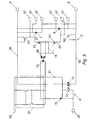
- Fig. 2 shows an embodiment of the present invention similar to that shown in Fig. 1 but with modifications to the control circuit 4 and the switch circuit 2.
- the LED 19 is connected to the pilot thyristor 15 and a drive circuit 51.
- the switch circuit is provided with additional resistors 53, 55 each of which is in series with the back-to-back LEDs 11.
- the switch circuit 2 is further provided with additional connectors 57 used to obtain electrical signals from a variety of points on the switch circuit 2.
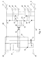
- Fig. 3 shows an SSR Circuit similar to that given in Fig. 2 which uses Silicon PNP transistors 61, 63 in place of the Schottky diodes 27, 29 shown in Fig. 2 .
- any other component functioning in a similar way to the Schottky diodes 27, 29 may be used in their place in circuit.
- transistors such as PNP Germanium transistors NPN Germanium transistors and NPN Silicon transistors.
- diodes such as Germanium diodes may be used.
- Fig 4 shows a circuit similar to that of Fig. 2 but with ferrite beads 71, 73 positioned on the leads 3 and 5 of thyristors 7 and 9 respectively.
- the ferrite beads act as a filter for high frequency noise and as such reduce the total noise in the circuit by 6db in comparison to similar circuits which do not contain the ferrite beads.
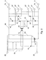
- FIG. 5 shows a circuit similar to that shown in Fig. 2 .
- resistors 67, 69 have been connected in parallel with Schottky diodes 27 and 29.
- Ferrite beads 71, 73 are also provided as in Fig.4 .
- the combination of resistors 67, 69 and ferrite beads 71, 73 further reduces the noise in the circuit by acting as a filter.
- the ferrite beads act to filter out high frequency noise from the circuit.
- noise can be reduced by around 18 db in comparison to similar circuits which do not contain the ferrite beads 71,73 or the resistors 67, 69.
- Fig. 6 shows a further embodiment of the invention, similar to that of Fig. 1 , in which like components are designated by like reference numerals.
- the Schottky diodes 27 and 29 of Fig. 1 have been replaced by FETs 33 and 35 (suitably MOSFETs) which are functionally equivalent to the diodes 27 and 29 of Fig. 1 ; i.e. the FETs 33 and 35 act as diodes.
- Operation of the FETs 33 and 35 is controlled by additional photovoltaic opto-couplers 37/38 and 39/40, each comprising an LED 37 and 39 in the control circuit 4 and a photovoltaic cell 38 and 40 in the switch circuit 2.
- a resistor 41 is connected across each of the photovoltaic cells 38 and 40.
- the control circuit 4 is configured such that suitable voltages are generated across each of the LEDs 19, 37 and 39 when the pilot thyristor 15 is turned on.
- the pilot thyristor 15 when the pilot thyristor 15 latches, it causes current to flow through the LEDs 19, 37 and 39 of each of the three photovoltaic opto-couplers 19/26, 37/38 and 39/40.
- the voltages generated by the photovoltaic cells 26, 38 and 40 turn cn the MOSFETs 21 and 23 (as before) and the FETs 33 and 35, so that current flows through the FET "diodes" 33 and 35 until the voltage across them is sufficiently high to turn on the thyristors 7 and 9.
- the FETs 33 and 35 are selected to have low "Rds On", so as to achieve a voltage drop of 0.1 volts or less. By this means, switching of the thyristors 7 and 9 occurs within 0.1 volts of true zero of the AC waveform and the noise generated is reduced to 15dB or less.
- Control of the device may be effected by an a.c. or d.c. voltage applied to the input terminals 25, typically having a value in the range 3 - 32 volts for a d.c. voltage.
- Fig. 7 shows an embodiment of the present invention similar to that shown in Fig. 6 .
- Schottky Diodes 27, 29 are retained in the circuit along with the FETs 33, 35.
Landscapes
- Electronic Switches (AREA)
- Relay Circuits (AREA)
- Alarm Systems (AREA)
- Control Of Combustion (AREA)
- Selective Calling Equipment (AREA)
Abstract
Description
- The present invention as it is defined is the independent claim relates to solid state relay circuits.
- In general, a relay is an electrical switching device in which operation of the switch is controlled by an electrical control signal applied to the relay. Conventional relays are electromechanical devices. A solid state relay (SSR), on the other hand, is comprised entirely of solid state components and, unlike electromagnetic relays, involves no mechanical movement to provide the required switching operation. An example of solid state relay is disclosed in the document
GB-A-2 062 372 - SSRs are commonly used to provide a safe interface between low voltage control circuits and high voltage, high current electrical equipment. Because it has no moving parts and is sealed, the SSR has become an essential component in a wide range of electrical equipment. However, the design of conventional SSRs suffers a serious disadvantage because it switches alternating current (AC) at random points in the sinusoidal waveform, causing bursts of electrical noise to be generated.
Improved designs seek to operate the switch at zero volts in the waveform, but there is still an uncertainty of at least +/- 1.8 volts in the switching voltage, which still produces considerable noise. - The increasing use of computers and other sensitive electronic systems, all of which are sensitive to mains-borne or radiated electrical interference, means that there is an increasing need to control electromagnetic noise such as that generated by SSRs. Existing European standards limit the maximum noise generated by electrical apparatus to 50 decibels (dB) throughout the frequency band of 30MHz to 1000MHz (radiated) and 150KHz to 30 MHz (conducted).
- Existing SSR designs fall well short of these standards, generating noise of the order of 120dB at 100kHz and thus requiring the use of complex and expensive filter circuits.
- One widely-used SSR design consists of a reversed, back-to-back pair of thyristors triggered by a crude, zero volts sensing device and can normally only be switched on when the voltage across the thyristors is greater than approximately 2V. The energy released by the switching action distorts the AC power waveform, typically by at least 2% at 100V. Such devices also switch on with a steep rise, increasing the harmonic content of the noise generated and so increasing the width of the frequency spectrum affected.
- It is an object of the present invention to provide an improved SSR in which the noise generated by operation of the SSR is substantially reduced.
- In accordance with a first aspect of the present invention there is provided a solid state relay comprising:
- a switch circuit including primary switch means for controlling an AC power supply, said primary switch means including thyristor means; and
- a control circuit for receiving a control input signal which controls the operation of said primary switch means; wherein
- said switch circuit and said control circuit are electrically isolated from one another and coupled to one another by first and second coupling means, said first coupling means being optical coupling means comprising first light emitting means in said switch circuit and optical switch means in said control circuit responsive to said first light emitting means,
and said second coupling means comprising signal emitting means in said control circuit and signal receiving means in said switch circuit responsive to said second signal emitting means; - said control circuit includes pilot switch means responsive to said optical switch means and said pilot switch means controls the operation of said second light emitting means;
- the light emitted by said first light emitting means varies with the AC supply voltage such that said pilot switch switches on said second signal emitting means at a predetermined AC supply voltage amplitude as said AC supply voltage approaches zero; and
- said photo-sensitive means operates in response to said second light emitting means to actuate said primary switching means.
- Preferably said primary switching means comprises a pair of inverse back-to-back thyristors.
- Alternatively, a pair of inverse back-to-back alternistors may be used.
- Further alternatively, a pair of inverse back-to-back triacs may be used.
- Optionally, the second coupling means may be magnetic coupling, electrostatic coupling or piezoelectric coupling.
- Preferably, said light emitting means comprise Light Emitting Diodes (LEDs).
- Preferably, said optical switch comprises a photo-transistor.
- Preferably, said second coupling means is an opto-coupling means, said second signal emitting means is a light emitting means and said signal receiving means is a photosensitive means.
- More preferably, said photo-sensitive means comprises a photovoltaic cell.
- Preferably, said pilot switch means comprises a thyristor.
- Preferably, the switch circuit includes secondary switch means responsive to said photo-sensitive means and adapted to trigger said primary switch means and to conduct said AC power supply in parallel with said primary switching means during a time interval between the switching on of said pilot switch and the AC power supply voltage amplitude reaching a predetermined minimum value at which the primary switch means takes over full conduction of the AC power supply.
- Preferably, said secondary switch means comprises a pair of gate-source coupled Field Effect Transistors (FETs) having their respective drains connected to the gates of the thyristor means of the primary switch means and first and second diode means connected between the gates of said thyristor means and AC supply terminals of the switch circuit.
- Preferably, the operation of said FETs is controlled by said photo-sensitive means.
- Preferably, said FETs are power Metal Oxide Semiconductor Field Effect Transistors.
- In one embodiment, said diode means comprise Schottky diodes.
- In a preferred embodiment, said diode means comprise transistors, the operation of which is controlled by further optical coupling means each comprising light emitting means in the control circuit, the operation of which is controlled by said pilot switch means, and photo-sensitive means (preferably a photovoltaic cell) in the switch circuit.
- In accordance with a second aspect of the present invention there is provided a solid state relay with means for sensing a zero volts crossing point in a waveform, said solid state relay including primary switching means and secondary switching means, said secondary switching means is adapted to trigger said primary switching means and to conduct an AC power supply in parallel with said primary switching means during a time interval between the switching on of a pilot switch and the AC power supply voltage amplitude reaching a predetermined minimum value at which the primary switch means takes over full conduction of the AC power supply.
- Preferably, said secondary switch means comprises a pair of gate-source coupled Field Effect Transistors (FETs) having their respective drains connected to the gates of the thyristor means of the primary switch means and first and second diode means connected between the gates of said thyristor means and AC supply terminals of the switch circuit.
- Embodiments of the present invention will now be described, by way of example only, with reference to the accompanying drawings of which:
-
Fig. 1 shows a first embodiment of an SSR circuit in accordance with the present invention; -
Fig. 2 shows an embodiment of an SSR circuit similar to that shown inFig. 1 but with a modified control circuit and additional connections to the switch circuit; -
Fig. 3 shows an embodiment of an SSR circuit similar to that shown inFig. 2 but with the Schottky diodes replaced with PNP transistors; -
Fig. 4 shows an embodiment of an SSR circuit similar to that shown inFig. 2 with ferrite beads connected to the thyristors; -
Fig. 5 shows an embodiment of an SSR circuit similar to that shown inFig. 2 with ferrite beads connected to the thyristors and resistors connected in parallel with the Schottky Diodes; -
Fig.6 shows a further embodiment of an SSR circuit in accordance with the present invention; and -
Fig. 7 shows an embodiment of an SSR circuit similar to that shown inFig. 6 with the Schottky diodes and Field Effect Transmitters (FETs). -
Fig. 1 shows a SSR circuit 1, comprising aswitch circuit 2 and acontrol circuit 4. Thecircuits - The
switch circuit 2 includes switching means comprising an inverse back-to-back pair ofthyristors AC input terminal 3 and anAC output terminal 5, so that operation of thethyristors terminals
The first opto-coupling means comprises an AC coupled, isolated opto-coupler consisting of a pair of back-to-back LEDs 11 in theswitch circuit 2, optically coupled to a photo-transistor 12 in thecontrol circuit 4. TheLEDs 11 and series current-limitingresistors 13 are connected in parallel with thethyristors - The second opto-coupling means comprises a photovoltaic opto-coupler consisting of an
LED 19 in thecontrol circuit 4, optically coupled to aphotovoltaic cell 26 in theswitch circuit 2. Alternatively, magnetic coupling, electrostatic coupling or piezoelectric coupling can be used instead of the second optical coupling means. - The operation of the
thyristors control circuit 4 and by further components of theswitch circuit 2, including opto-couplers 11/12 and 19/26, a pair of gate-source coupledpower MOSFETs thyristors Vf Schottky diodes thyristors AC terminals - The
MOSFETS photovoltaic cell 26, ableed resistor 18 being connected in parallel with thephotovoltaic cell 26 and conduct across the zero point in the AC voltage signal from a positive higher that the cut off voltage of the thyristor in the positive half of the cycle to a negative voltage lower than the voltage at which the thyristor is switched on in the negative half of the cycle. - The
control circuit 4 includes apilot thyristor 15 connected in series with theLED 19 of photovoltaic opto-coupler 19/26 andresistor 17 acrossinput terminals 25. The photo-transistor 12 of opto-coupler 11/12 is connected in series with pull-up resistor 20, also across theterminals 25. The gate of thepilot thyristor 15 is connected to a point between the photo-transistor 12 and pull-up resistor 20. In use, a control-input voltage is applied to theterminals 25. - When the AC voltage across the
AC terminals back LEDs 11, the photo-transistor 12 optically coupled thereto is conducting, thereby holding off thepilot thyristor 15. As the AC waveform approaches zero (in this example, 0.8 volts before zero), the photo-transistor 12 turns off, allowing the pull-up resistor 20 to conduct current into the gate of thepilot thyristor 15, turning it on. Thepilot thyristor 15 then latches on, causing current to flow through theLED 19 of the photovoltaic opto-coupler 19/26. The voltage generated by thephotovoltaic cell 26 turns on theMOSFETs Schottky diodes thyristors - The SSR of
Fig. 1 provides improved zero crossing detection by sensing an approaching zero crossing at about 0.7 volts before zero. This enables pre-arming of the thyristor firing sequence and ensures switching at or very close to true zero, reducing noise by about 20dB. - The
thyristors - The
MOSFETs thyristors MOSFETs - In relay circuits in which the MOSFETs conducted only in the forward bias direction, the time interval between conduction of the MOSFETs can result in switching at a point in the cycle where there is a large AC current if the AC current and voltage are out of phase, which generates a large spike of noise. In such cases, it is necessary to remove the noise using a device called a snubber. In the present invention,
MOSFETs MOSFET 23 toMOSFET 22 and vice versa and no associated time delay. Therefore, the level of noise in the circuit is not affected if the AC voltage and AC current are out of phase. - The embodiment of
Fig. 1 may reduce the noise level to about 48dB at 100kHz, which is just within the 50dB limit of current European standards. This residual noise is due in part to the voltage drop of about 0.2 to 0.4 volts across each of theSchottky diodes -
Figs. 2 to 5 provide additional means for noise reduction in circuits similar to that shown inFig.1 . In the following embodiment, identical reference numerals are used when describing identical components. -
Fig. 2 shows an embodiment of the present invention similar to that shown inFig. 1 but with modifications to thecontrol circuit 4 and theswitch circuit 2. In this example theLED 19 is connected to thepilot thyristor 15 and adrive circuit 51. The switch circuit is provided withadditional resistors back LEDs 11. Theswitch circuit 2 is further provided withadditional connectors 57 used to obtain electrical signals from a variety of points on theswitch circuit 2. -
Fig. 3 shows an SSR Circuit similar to that given inFig. 2 which usesSilicon PNP transistors Schottky diodes Fig. 2 . - It will be appreciated that any other component functioning in a similar way to the
Schottky diodes -
Fig 4 . shows a circuit similar to that ofFig. 2 but withferrite beads leads thyristors - The embodiment of the present invention in
Fig. 5 shows a circuit similar to that shown inFig. 2 . In this example,resistors Schottky diodes Ferrite beads Fig.4 . The combination ofresistors ferrite beads ferrite beads resistors -
Fig. 6 shows a further embodiment of the invention, similar to that ofFig. 1 , in which like components are designated by like reference numerals. - In
Fig. 6 , theSchottky diodes Fig. 1 have been replaced byFETs 33 and 35 (suitably MOSFETs) which are functionally equivalent to thediodes Fig. 1 ; i.e. theFETs FETs couplers 37/38 and 39/40, each comprising anLED control circuit 4 and aphotovoltaic cell switch circuit 2. Aresistor 41 is connected across each of thephotovoltaic cells control circuit 4 is configured such that suitable voltages are generated across each of theLEDs pilot thyristor 15 is turned on. - In this embodiment, when the
pilot thyristor 15 latches, it causes current to flow through theLEDs couplers 19/26, 37/38 and 39/40. The voltages generated by thephotovoltaic cells MOSFETs 21 and 23 (as before) and theFETs thyristors - The
FETs thyristors - Control of the device may be effected by an a.c. or d.c. voltage applied to the
input terminals 25, typically having a value in the range 3 - 32 volts for a d.c. voltage. -
Fig. 7 shows an embodiment of the present invention similar to that shown inFig. 6 . In this exampleSchottky Diodes FETs - Improvements and modifications may be incorporated without departing from the scope of the invention.
Claims (17)
- A solid state relay (1) comprising:a switch circuit (2) including primary switch means for controlling an AC power supply (3,5), said primary switch means including thyristor means (7,9); anda control circuit (4) for receiving a control input signal which controls the operation of said primary switch means; whereinsaid switch circuit (2) and said control circuit (4) are electrically isolated from one another and coupled to one another by first and second coupling means (11,12, 19,26),said first coupling means (11,12) being optical coupling means comprising first light emitting means (11) in said switch circuit (2) and optical switch means (12) in said control circuit (4), responsive to said first light emitting means (11),and said second coupling means (19,26) comprising second signal emitting means (19) in said control circuit (4) and signal receiving means (26) in said switch circuit (2) responsive to said second signal emitting means (26);said control circuit (4) includes pilot switch means (15) responsive to said optical switch means (12) and said pilot switch means (15) controls the operation of said second signal emitting means (19);the light emitted by said first light emitting means (11) varies with the AC supply voltage (3,5) such that said pilot switch (15) switches on said second signal emitting means (19) at a predetermined AC supply voltage amplitude as said AC supply voltage (3,5) approaches zero; andsaid signal receiving means (26) operates in response to said second light emitting means (19) to actuate said primary switching means (7,9); and whereinthe switch circuit (2) includes secondary switch means (21,23) responsive to said signal receiving means (26) and adapted to trigger said primary switch means (7,9) and to conduct said AC power supply (3,5) in parallel with said primary switching means (7,9) during a time interval between the switching on of said pilot switch (15) and the AC power supply (3,5) voltage amplitude reaching a predetermined minimum value at which the primary switch means takes over full conduction of the AC power supply (3,5).
- A solid state relay as claimed in claim 1 wherein said primary switching means comprises a pair of inverse back-to-back thyristors (7,9).
- A solid state relay as claimed in claim 1 wherein said primary switching means comprises a pair of inverse back-to-back alternistors.
- A solid state relay as claimed in claim 1 wherein said primary switching means comprises a pair of inverse back-to-back triacs.
- A solid state relay as claimed in any preceding claim wherein the second coupling means is an optical coupling or a magnetic coupling or an electrostatic coupling or a piezoelectric coupling.
- A solid state relay as claimed in any preceding claim wherein said light emitting means (11,19) are Light Emitting Diodes (LEDs).
- A solid state relay as claimed in any preceding claim wherein said optical switch (12) means comprises a photo-transistor.
- A solid state relay as claimed in any preceding claim wherein said second coupling means is an opto-coupling means, said second signal emitting means (19) is a light emitting means and said signal receiving means (26) is a photosensitive means.
- A solid state relay as claimed in claim 8 wherein said photosensitive means comprises a photovoltaic cell (26).
- A solid state relay as claimed in any preceding claim wherein said pilot switch means (15) comprises a thyristor.
- A solid state relay as claimed in any preceding claim wherein said secondary switch means (21,23) comprises a pair of gate-source coupled Field Effect Transistors (FETs) having their respective drains connected to the gates of the thyristor means (7,9) of the primary switch means and first and second diode means (27,29) connected between the gates of said thyristor means (7,9) and AC supply terminals (3,5) of the switch circuit (2).
- A solid state relay as claimed in any claim 11 wherein the operation of said FETs (21,23) is controlled by said signal receiving means (26).
- A solid state relay as claimed in any claim 11 or claim 12 wherein said FETs (21,23) are power Metal Oxide Semiconductor Field Effect Transistors.
- A solid state relay as claimed in any of claims 11 to 13 wherein said diode means (27,29) comprise Schottky diodes.
- A solid state relay as claimed in any of claims 11 to 14 wherein said diode means comprise transistors (33,35), the operation of which is controlled by further optical coupling means (37,38,39,40) each comprising light emitting means (37,39) in the control circuit (4), the operation of which is controlled by said pilot switch means (15), and photo-sensitive means (38,40) (preferably a photovoltaic cell) in the switch circuit (2).
- A solid state relay with means for sensing a zero volts crossing point in a waveform, said solid state relay including primary switching means (7,9) and secondary switching means (21,23), said secondary switching means (21,23) is adapted to trigger said primary switching means (7,9) and to conduct an AC power supply (3,5) in parallel with said primary switching means (7,9) during a time interval between the switching on of a pilot switch (15) and the AC power supply voltage (3,5) amplitude reaching a predetermined minimum value at which the primary switch means (7,9) takes over full conduction of the AC power supply (3,5).
- A solid state relay as claimed in claim 16 wherein, said secondary switch means (21,23) comprises a pair of gate-source coupled Field Effect Transistors (FETs) having their respective drains connected to the gates of the thyristor means (7,9) of the primary switch means and first and second diode means (27,29) connected between the gates of said thyristor means (7,9) and AC supply terminals (3,5) of the switch circuit (2).
Applications Claiming Priority (4)
| Application Number | Priority Date | Filing Date | Title |
|---|---|---|---|
| GB0004618 | 2000-02-29 | ||
| GB0004618A GB0004618D0 (en) | 2000-02-29 | 2000-02-29 | Solid state relay |
| GB0025608A GB0025608D0 (en) | 2000-10-19 | 2000-10-19 | Solid state relay |
| GB0025608 | 2000-10-19 |
Publications (3)
| Publication Number | Publication Date |
|---|---|
| EP1130777A2 EP1130777A2 (en) | 2001-09-05 |
| EP1130777A3 EP1130777A3 (en) | 2002-11-27 |
| EP1130777B1 true EP1130777B1 (en) | 2008-07-02 |
Family
ID=26243743
Family Applications (1)
| Application Number | Title | Priority Date | Filing Date |
|---|---|---|---|
| EP01301790A Expired - Lifetime EP1130777B1 (en) | 2000-02-29 | 2001-02-27 | Solid state relay |
Country Status (3)
| Country | Link |
|---|---|
| EP (1) | EP1130777B1 (en) |
| AT (1) | ATE400086T1 (en) |
| DE (1) | DE60134597D1 (en) |
Families Citing this family (3)
| Publication number | Priority date | Publication date | Assignee | Title |
|---|---|---|---|---|
| RU2241308C2 (en) * | 2003-01-08 | 2004-11-27 | Открытое акционерное общество "Новосибирское авиационное производственное объединение им. В.П. Чкалова" | Three-phase switching unit |
| RU2241307C2 (en) * | 2003-01-08 | 2004-11-27 | Открытое акционерное общество "Новосибирское авиационное производственное объединение им. В.П. Чкалова" | Three-phase switching unit |
| US9413160B2 (en) | 2012-04-19 | 2016-08-09 | Freescale Semiconductor, Inc. | Protection circuit and a gate driving circuitry |
Family Cites Families (4)
| Publication number | Priority date | Publication date | Assignee | Title |
|---|---|---|---|---|
| GB2062372B (en) * | 1979-10-20 | 1984-05-10 | Plessey Co Ltd | Thyristor control circuits |
| DE4026679A1 (en) * | 1990-08-23 | 1992-02-27 | Siemens Ag | On=off switching device for compensation capacitors - consists of two thyristors in antiparallel energised by control dependent on voltage difference |
| DE4313882C1 (en) * | 1993-04-28 | 1994-08-04 | Electromatic Ind A S | Semiconductor relay for switching ac load |
| FI110370B (en) * | 1998-07-31 | 2002-12-31 | Lexel Finland Ab Oy | Arrangements for the elimination of radio interference in an electronic power regulator |
-
2001
- 2001-02-27 AT AT01301790T patent/ATE400086T1/en not_active IP Right Cessation
- 2001-02-27 DE DE60134597T patent/DE60134597D1/en not_active Expired - Lifetime
- 2001-02-27 EP EP01301790A patent/EP1130777B1/en not_active Expired - Lifetime
Also Published As
| Publication number | Publication date |
|---|---|
| ATE400086T1 (en) | 2008-07-15 |
| DE60134597D1 (en) | 2008-08-14 |
| EP1130777A3 (en) | 2002-11-27 |
| EP1130777A2 (en) | 2001-09-05 |
Similar Documents
| Publication | Publication Date | Title |
|---|---|---|
| CA2427039C (en) | High speed bi-directional solid state switch | |
| US6794951B2 (en) | Solid state RF power switching network | |
| US4217618A (en) | Thyristor firing circuit module with integral optical isolation, dv/dt limitation, and bidirectional voltage transient suppression | |
| US3530310A (en) | Touch activated dc switch and programmer array | |
| EP1456951A1 (en) | Half-bridge driver and power conversion system with such driver | |
| CN106130322B (en) | Gate driving circuit for reducing parasitic coupling | |
| EP1254516B1 (en) | High power modulator | |
| US20100135047A1 (en) | High-Voltage Modulator System | |
| US5557494A (en) | Drive circuit of an electromagnetic device | |
| US12335068B2 (en) | Multi-channel digital isolator with integrated configurable pulse width modulation interlock protection | |
| US7227280B2 (en) | Isolated control apparatus incorporating light controlled power semiconductors | |
| US4425518A (en) | High voltage field effect transistor pulse apparatus | |
| EP1130777A2 (en) | Solid state relay | |
| US20140035655A1 (en) | Matrix-stages solid state ultrafast switch | |
| WO1997043832A1 (en) | Insulated gate bipolar transistor control | |
| CN220022605U (en) | Driving circuit and current transformer | |
| US3411020A (en) | Power turn-off timer | |
| US3015039A (en) | Fail-safe control apparatus | |
| KR100581490B1 (en) | Drive system of high pressure switching system | |
| US12407333B1 (en) | Method of parasitic oscillation reduction and parasitic oscillation immune resonant converter | |
| CN112154594B (en) | Half-bridge electronic device comprising two systems for optimizing the dead time between switching operations of a high-level switch and a low-level switch | |
| CN111681910B (en) | Coil driving device of electromagnetic contactor | |
| WO2021111823A1 (en) | Gate drive circuit and power conversion device | |
| US20260106601A1 (en) | Configurable fast transition pulse power supply unit | |
| US4295057A (en) | Dual signal control system |
Legal Events
| Date | Code | Title | Description |
|---|---|---|---|
| PUAI | Public reference made under article 153(3) epc to a published international application that has entered the european phase |
Free format text: ORIGINAL CODE: 0009012 |
|
| AK | Designated contracting states |
Kind code of ref document: A2 Designated state(s): AT BE CH CY DE DK ES FI FR GB GR IE IT LI LU MC NL PT SE TR |
|
| AX | Request for extension of the european patent |
Free format text: AL;LT;LV;MK;RO;SI |
|
| PUAL | Search report despatched |
Free format text: ORIGINAL CODE: 0009013 |
|
| RIC1 | Information provided on ipc code assigned before grant |
Free format text: 7H 03K 17/725 A, 7H 03K 17/722 B, 7H 03K 17/79 B, 7H 03K 17/13 B |
|
| AK | Designated contracting states |
Kind code of ref document: A3 Designated state(s): AT BE CH CY DE DK ES FI FR GB GR IE IT LI LU MC NL PT SE TR |
|
| AX | Request for extension of the european patent |
Free format text: AL;LT;LV;MK;RO;SI |
|
| 17P | Request for examination filed |
Effective date: 20030417 |
|
| AKX | Designation fees paid |
Designated state(s): AT BE CH CY DE DK ES FI FR GB GR IE IT LI LU MC NL PT SE TR |
|
| GRAP | Despatch of communication of intention to grant a patent |
Free format text: ORIGINAL CODE: EPIDOSNIGR1 |
|
| GRAS | Grant fee paid |
Free format text: ORIGINAL CODE: EPIDOSNIGR3 |
|
| RAP1 | Party data changed (applicant data changed or rights of an application transferred) |
Owner name: ROOT 2 LIMITED |
|
| GRAA | (expected) grant |
Free format text: ORIGINAL CODE: 0009210 |
|
| AK | Designated contracting states |
Kind code of ref document: B1 Designated state(s): AT BE CH CY DE DK ES FI FR GB GR IE IT LI LU MC NL PT SE TR |
|
| REG | Reference to a national code |
Ref country code: GB Ref legal event code: FG4D |
|
| REG | Reference to a national code |
Ref country code: CH Ref legal event code: EP |
|
| REF | Corresponds to: |
Ref document number: 60134597 Country of ref document: DE Date of ref document: 20080814 Kind code of ref document: P |
|
| REG | Reference to a national code |
Ref country code: IE Ref legal event code: FG4D |
|
| PG25 | Lapsed in a contracting state [announced via postgrant information from national office to epo] |
Ref country code: NL Free format text: LAPSE BECAUSE OF FAILURE TO SUBMIT A TRANSLATION OF THE DESCRIPTION OR TO PAY THE FEE WITHIN THE PRESCRIBED TIME-LIMIT Effective date: 20080702 |
|
| NLV1 | Nl: lapsed or annulled due to failure to fulfill the requirements of art. 29p and 29m of the patents act | ||
| PG25 | Lapsed in a contracting state [announced via postgrant information from national office to epo] |
Ref country code: ES Free format text: LAPSE BECAUSE OF FAILURE TO SUBMIT A TRANSLATION OF THE DESCRIPTION OR TO PAY THE FEE WITHIN THE PRESCRIBED TIME-LIMIT Effective date: 20081013 Ref country code: PT Free format text: LAPSE BECAUSE OF FAILURE TO SUBMIT A TRANSLATION OF THE DESCRIPTION OR TO PAY THE FEE WITHIN THE PRESCRIBED TIME-LIMIT Effective date: 20081202 |
|
| PG25 | Lapsed in a contracting state [announced via postgrant information from national office to epo] |
Ref country code: FI Free format text: LAPSE BECAUSE OF FAILURE TO SUBMIT A TRANSLATION OF THE DESCRIPTION OR TO PAY THE FEE WITHIN THE PRESCRIBED TIME-LIMIT Effective date: 20080702 Ref country code: AT Free format text: LAPSE BECAUSE OF FAILURE TO SUBMIT A TRANSLATION OF THE DESCRIPTION OR TO PAY THE FEE WITHIN THE PRESCRIBED TIME-LIMIT Effective date: 20080702 |
|
| PG25 | Lapsed in a contracting state [announced via postgrant information from national office to epo] |
Ref country code: BE Free format text: LAPSE BECAUSE OF FAILURE TO SUBMIT A TRANSLATION OF THE DESCRIPTION OR TO PAY THE FEE WITHIN THE PRESCRIBED TIME-LIMIT Effective date: 20080702 |
|
| PG25 | Lapsed in a contracting state [announced via postgrant information from national office to epo] |
Ref country code: DK Free format text: LAPSE BECAUSE OF FAILURE TO SUBMIT A TRANSLATION OF THE DESCRIPTION OR TO PAY THE FEE WITHIN THE PRESCRIBED TIME-LIMIT Effective date: 20080702 |
|
| PLBE | No opposition filed within time limit |
Free format text: ORIGINAL CODE: 0009261 |
|
| STAA | Information on the status of an ep patent application or granted ep patent |
Free format text: STATUS: NO OPPOSITION FILED WITHIN TIME LIMIT |
|
| 26N | No opposition filed |
Effective date: 20090403 |
|
| PG25 | Lapsed in a contracting state [announced via postgrant information from national office to epo] |
Ref country code: MC Free format text: LAPSE BECAUSE OF NON-PAYMENT OF DUE FEES Effective date: 20090228 |
|
| REG | Reference to a national code |
Ref country code: CH Ref legal event code: PL |
|
| PG25 | Lapsed in a contracting state [announced via postgrant information from national office to epo] |
Ref country code: CH Free format text: LAPSE BECAUSE OF NON-PAYMENT OF DUE FEES Effective date: 20090228 Ref country code: LI Free format text: LAPSE BECAUSE OF NON-PAYMENT OF DUE FEES Effective date: 20090228 |
|
| REG | Reference to a national code |
Ref country code: IE Ref legal event code: MM4A |
|
| PG25 | Lapsed in a contracting state [announced via postgrant information from national office to epo] |
Ref country code: IE Free format text: LAPSE BECAUSE OF NON-PAYMENT OF DUE FEES Effective date: 20090227 Ref country code: SE Free format text: LAPSE BECAUSE OF FAILURE TO SUBMIT A TRANSLATION OF THE DESCRIPTION OR TO PAY THE FEE WITHIN THE PRESCRIBED TIME-LIMIT Effective date: 20081002 |
|
| PG25 | Lapsed in a contracting state [announced via postgrant information from national office to epo] |
Ref country code: GR Free format text: LAPSE BECAUSE OF FAILURE TO SUBMIT A TRANSLATION OF THE DESCRIPTION OR TO PAY THE FEE WITHIN THE PRESCRIBED TIME-LIMIT Effective date: 20081003 |
|
| PG25 | Lapsed in a contracting state [announced via postgrant information from national office to epo] |
Ref country code: LU Free format text: LAPSE BECAUSE OF NON-PAYMENT OF DUE FEES Effective date: 20090227 |
|
| PG25 | Lapsed in a contracting state [announced via postgrant information from national office to epo] |
Ref country code: TR Free format text: LAPSE BECAUSE OF FAILURE TO SUBMIT A TRANSLATION OF THE DESCRIPTION OR TO PAY THE FEE WITHIN THE PRESCRIBED TIME-LIMIT Effective date: 20080702 |
|
| PG25 | Lapsed in a contracting state [announced via postgrant information from national office to epo] |
Ref country code: CY Free format text: LAPSE BECAUSE OF FAILURE TO SUBMIT A TRANSLATION OF THE DESCRIPTION OR TO PAY THE FEE WITHIN THE PRESCRIBED TIME-LIMIT Effective date: 20080702 |
|
| PGFP | Annual fee paid to national office [announced via postgrant information from national office to epo] |
Ref country code: IT Payment date: 20140224 Year of fee payment: 14 Ref country code: FR Payment date: 20140131 Year of fee payment: 14 |
|
| REG | Reference to a national code |
Ref country code: FR Ref legal event code: ST Effective date: 20151030 |
|
| PG25 | Lapsed in a contracting state [announced via postgrant information from national office to epo] |
Ref country code: IT Free format text: LAPSE BECAUSE OF NON-PAYMENT OF DUE FEES Effective date: 20150227 |
|
| PG25 | Lapsed in a contracting state [announced via postgrant information from national office to epo] |
Ref country code: FR Free format text: LAPSE BECAUSE OF NON-PAYMENT OF DUE FEES Effective date: 20150302 |
|
| PGFP | Annual fee paid to national office [announced via postgrant information from national office to epo] |
Ref country code: DE Payment date: 20160218 Year of fee payment: 16 |
|
| PGFP | Annual fee paid to national office [announced via postgrant information from national office to epo] |
Ref country code: GB Payment date: 20160217 Year of fee payment: 16 |
|
| REG | Reference to a national code |
Ref country code: DE Ref legal event code: R119 Ref document number: 60134597 Country of ref document: DE |
|
| GBPC | Gb: european patent ceased through non-payment of renewal fee |
Effective date: 20170227 |
|
| PG25 | Lapsed in a contracting state [announced via postgrant information from national office to epo] |
Ref country code: DE Free format text: LAPSE BECAUSE OF NON-PAYMENT OF DUE FEES Effective date: 20170901 |
|
| PG25 | Lapsed in a contracting state [announced via postgrant information from national office to epo] |
Ref country code: GB Free format text: LAPSE BECAUSE OF NON-PAYMENT OF DUE FEES Effective date: 20170227 |