EP1130768A2 - A low supply voltage analog multiplier - Google Patents
A low supply voltage analog multiplier Download PDFInfo
- Publication number
- EP1130768A2 EP1130768A2 EP01100815A EP01100815A EP1130768A2 EP 1130768 A2 EP1130768 A2 EP 1130768A2 EP 01100815 A EP01100815 A EP 01100815A EP 01100815 A EP01100815 A EP 01100815A EP 1130768 A2 EP1130768 A2 EP 1130768A2
- Authority
- EP
- European Patent Office
- Prior art keywords
- cell
- multiplier
- transistor
- pair
- transistors
- Prior art date
- Legal status (The legal status is an assumption and is not a legal conclusion. Google has not performed a legal analysis and makes no representation as to the accuracy of the status listed.)
- Withdrawn
Links
Images

Classifications
-
- G—PHYSICS
- G06—COMPUTING OR CALCULATING; COUNTING
- G06G—ANALOGUE COMPUTERS
- G06G7/00—Devices in which the computing operation is performed by varying electric or magnetic quantities
- G06G7/12—Arrangements for performing computing operations, e.g. operational amplifiers specially adapted therefor
- G06G7/16—Arrangements for performing computing operations, e.g. operational amplifiers specially adapted therefor for multiplication or division
- G06G7/163—Arrangements for performing computing operations, e.g. operational amplifiers specially adapted therefor for multiplication or division using a variable impedance controlled by one of the input signals, variable amplification or transfer function
-
- H—ELECTRICITY
- H03—ELECTRONIC CIRCUITRY
- H03D—DEMODULATION OR TRANSFERENCE OF MODULATION FROM ONE CARRIER TO ANOTHER
- H03D7/00—Transference of modulation from one carrier to another, e.g. frequency-changing
- H03D7/14—Balanced arrangements
- H03D7/1408—Balanced arrangements with diodes
-
- H—ELECTRICITY
- H03—ELECTRONIC CIRCUITRY
- H03D—DEMODULATION OR TRANSFERENCE OF MODULATION FROM ONE CARRIER TO ANOTHER
- H03D7/00—Transference of modulation from one carrier to another, e.g. frequency-changing
- H03D7/14—Balanced arrangements
- H03D7/1425—Balanced arrangements with transistors
- H03D7/1433—Balanced arrangements with transistors using bipolar transistors
-
- H—ELECTRICITY
- H03—ELECTRONIC CIRCUITRY
- H03D—DEMODULATION OR TRANSFERENCE OF MODULATION FROM ONE CARRIER TO ANOTHER
- H03D7/00—Transference of modulation from one carrier to another, e.g. frequency-changing
- H03D7/14—Balanced arrangements
- H03D7/1425—Balanced arrangements with transistors
- H03D7/1491—Arrangements to linearise a transconductance stage of a mixer arrangement
-
- H—ELECTRICITY
- H03—ELECTRONIC CIRCUITRY
- H03D—DEMODULATION OR TRANSFERENCE OF MODULATION FROM ONE CARRIER TO ANOTHER
- H03D2200/00—Indexing scheme relating to details of demodulation or transference of modulation from one carrier to another covered by H03D
- H03D2200/0041—Functional aspects of demodulators
- H03D2200/0086—Reduction or prevention of harmonic frequencies
Definitions
- This invention relates to an improved analog multiplier, wherein enhanced accuracy at low supply voltages is achieved for but a minimal increase in circuit area.
- the invention relates to a low supply voltage analog multiplier which comprises a pair of differential cells, with each cell being comprised of a pair of bipolar transistors with coupled emitters, a first transistor of each cell receiving an input signal on its base terminal and having its collector terminal coupled to a first voltage reference through a bias member.
- analog multipliers are used for balancing modulators, as well as in phase detectors and the like devices.
- digital signal converters having a quadratic type of transfer function, it is essential that an analog multiplier be employed to produce a proportional signal to two analog input signals which are identical with each other.
- a differential stage with coupled emitters may constitute an elementary multiplier cell capable of generating (differential) collector output currents which are dependent on a differential voltage applied to its inputs, e,g, to the base terminals of a bipolar transistor pair forming the differential stage.
- analog multipliers By duplicating an elementary cell, analog multipliers can be obtained which can operate between two or among four quadrants of a differential plane of input voltages.
- a typical cell of a four-quadrant multiplier is referred to in the literature as Gilbert's cell or circuit.
- a pre-distortion stage is connected in, upstream of the analog multiplier, to introduce pre-distortion in the input signal and compensate for the hyperbolic tangent transfer characteristic of the multiplier cell.
- the pre-distortion stage is usually in the form of a diode-configured bipolar transistor whereby a current input signal is forced to produce a voltage output signal having a transfer function which is the reciprocal of the hyperbolic tangent.
- Multipliers of this type are known in the literature, e.g. from a book "Analog Integrated Circuits -- Analysis and Design” by Paul R. Grey and Robert G. Meyer, McGraw-Hill, which contains a detailed description and an analysis of these circuits under Chapter 10, pages 694-705 foll..
- the basic characteristics expected of an analog multipliers include: high accuracy, relatively low power consumption, and moderate circuit complexity.
- the common mode output voltage varies as the potential at a central node of the multiplier, which potential is equal to the half sum of the inputs, and this makes conventional multipliers too readily affected by sharp variations in the input signal.
- the underlying technical problem of this invention is to provide an analog multiplier structure of uniquely simple constructional and functional features, which can be supplied a very low supply voltage and allows a plurality of stages to be cascade connected to enhance input linearity while retaining a fair speed, thereby overcoming the limitations of prior solutions.
- Another object of this invention is to provide an analog multiplier which is highly reliable in operation and comparatively inexpensive to manufacture.
- the principle on which this invention stands is one of arranging in a multiplier in which the dynamic of the signal at the heads of the compressor and of the expander is constant regardless of the multiplier value of gain. This ensures a multiplier harmonic distortion which is constant and independent of the multiply factor of the stage.
- an analog multiplier as previously indicated and characterized in that the second transistor of each cell is a diode configuration, and that the cells are interconnected at a common node corresponding to the base terminals of the second transistors in each pair.
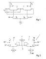
- the structure 1 includes a first circuit portion 10 and a second circuit portion 11 connected to each other. These portions 10, 11 are essentially differential cells interconnected into a fully differential configuration.
- the first portion or cell 10 comprises a first bipolar transistor 2 which has a control terminal, being its base terminal, arranged to receive a first input signal Vin+.
- the first transistor 2 has a conduction terminal, being its collector terminal, connected to a first supply voltage reference Vcc through a diode 4 which is forward biased to the power supply.
- the collector node forms a first output terminal OUT- of the multiplier 1.
- the portion 10 further comprises a second bipolar transistor 3 having its emitter terminal connected to the emitter terminal of the first transistor 2.
- the emitter terminals of the first 2 and the second 3 transistors are connected to a second voltage reference GND through a current generator 5 which is to deliver a current 2I.
- the base and collector terminals of the second transistor 3 are interconnected, thus providing a diode configuration of the transistor.
- the base terminal of the second transistor 3 also forms a node A of interconnection for the first 10 and the second 11 cells of the circuit structure 1.
- the second cell 11 is similar to the first and connected to the first cell 10 in mirror-image relationship.
- the second cell 11 also comprises a first bipolar transistor 6 having a base terminal arranged to receive a second input signal Vin-.
- the first transistor 6 of the second cell 11 has a collector terminal connected to the first supply voltage reference Vcc through a diode 8 which is forward biased to the power supply.
- the collector node forms a second output terminal OUT+ of the multiplier 1.
- the second cell 11 further comprises a second bipolar transistor 7 having its emitter terminal connected to the emitter terminal of the first transistor 6.
- the emitter terminals of the first 6 and the second 7 transistors of the second cell 11 are connected to the second voltage reference GND through a current generator 9 which is to deliver a current 2I.
- the base and collector terminals of the second transistor 7 are interconnected, thus providing a diode configuration of the transistor.
- a current generator I2 delivering a current 2I to the node A, is connected between the node A interconnecting the cells 10, 11 and the first voltage reference Vcc.
- the transistors of the structure 1 are all npn bipolar transistors. However, the circuit could be arranged to comprise pnp transistors instead.
- the second transistor 7 of the second cell 11 may be slightly larger than the second transistor 3 of the first cell 10, e.g. to a dimensional ratio of 1.8.
- the transconductance value of the transistors 3 and 7 can be made to change, thus varying the gain value of the multiplier.
- the multiplier of this invention has a DC output voltage Vout which remains fixed as the current I of the bias generators varies, this being an optimum condition for a minimal harmonic distortion.
- the multiplier of this invention is suitable for connection in cascade with other multipliers of the same type; in this way, input linearity is enhanced.
- the load diodes 4, 8 would then be connected to the first cell and the last cell in the cascade.
- the multiplier according to this invention does solve the technical problem, and offers a number of advantages, foremost among which is that the multiplier can be supplied very low voltages, below 3 V.
- the common mode voltage is the difference in base-emitter voltage drop between the transistors 2 and 3 of Figure 2.
- the circuit structure of this invention is quite simple, and has shown to be extremely fast.
Landscapes
- Engineering & Computer Science (AREA)
- Power Engineering (AREA)
- Physics & Mathematics (AREA)
- Mathematical Physics (AREA)
- Theoretical Computer Science (AREA)
- Software Systems (AREA)
- Computer Hardware Design (AREA)
- General Physics & Mathematics (AREA)
- Amplifiers (AREA)
- Control Of Motors That Do Not Use Commutators (AREA)
- Control Of Eletrric Generators (AREA)
Abstract
Description
Claims (9)
- A low supply voltage analog multiplier which comprises a pair of differential cells (10,11), with each cell being comprised of a pair of bipolar transistors (2,3;6,7) with coupled emitters, a first transistor (2,6) of each cell (10,11) receiving an input signal (Vin+,Vin-) on its base terminal and having its collector terminal coupled to a first voltage reference (Vcc) through a bias member (4,8), characterized in that the second transistor (3,7) of each cell is a diode configuration, and that the cells are interconnected at a common node (A) corresponding to the base terminals of the second transistors (3,7) in each pair.
- A multiplier according to Claim 1, characterized in that it includes a current generator (I2) connected between said first voltage reference and said common node (A).
- A multiplier according to Claim 2, characterized in that, connected between each coupled emitter and a second voltage reference (GND), is a bias current generator (5,9) adapted to deliver a current (2I) equal to the current from said current generator (I2) connected to said common node (A).
- A multiplier according to Claim 1, characterized in that the collector terminals of the first transistors (2,6) in each pair form the differential outputs (OUT-,OUT+) of the multiplier.
- A multiplier according to Claim 1, characterized in that it is a fully differential configuration.
- A multiplier according to Claim 1, characterized in that all the transistors are npn bipolar transistors.
- A multiplier according to Claim 1, characterized in that said bias member comprises a diode (4,8) which is forward biased to the first supply voltage reference.
- A multiplier according to Claim 1, characterized in that it is connected in cascade with multipliers in the same structure, a loading diode being associated with the first cell in the cascade and the last cell in the cascade.
- A multiplier according to Claim 1, characterized in that the second transistor (7) of the second cell (11) exceeds in area the second transistor (3) of the first cell (10).
Applications Claiming Priority (2)
| Application Number | Priority Date | Filing Date | Title |
|---|---|---|---|
| ITMI200391 | 2000-02-29 | ||
| IT2000MI000391A IT1316688B1 (en) | 2000-02-29 | 2000-02-29 | LOW POWER VOLTAGE ANALOGUE MULTIPLIER |
Publications (2)
| Publication Number | Publication Date |
|---|---|
| EP1130768A2 true EP1130768A2 (en) | 2001-09-05 |
| EP1130768A3 EP1130768A3 (en) | 2003-09-17 |
Family
ID=11444257
Family Applications (1)
| Application Number | Title | Priority Date | Filing Date |
|---|---|---|---|
| EP01100815A Withdrawn EP1130768A3 (en) | 2000-02-29 | 2001-01-15 | A low supply voltage analog multiplier |
Country Status (4)
| Country | Link |
|---|---|
| US (1) | US7061300B2 (en) |
| EP (1) | EP1130768A3 (en) |
| JP (1) | JP3548127B2 (en) |
| IT (1) | IT1316688B1 (en) |
Families Citing this family (2)
| Publication number | Priority date | Publication date | Assignee | Title |
|---|---|---|---|---|
| JP3598973B2 (en) * | 2001-01-10 | 2004-12-08 | ソニー株式会社 | Variable gain circuit |
| US8179198B2 (en) * | 2009-07-31 | 2012-05-15 | Texas Instruments Incorporated | Variable gain amplifier having automatic power consumption optimization |
Family Cites Families (13)
| Publication number | Priority date | Publication date | Assignee | Title |
|---|---|---|---|---|
| SE457922B (en) * | 1987-06-18 | 1989-02-06 | Ericsson Telefon Ab L M | DEVICE FOR ACTIVE FILTER AND USE THEREOF |
| US4978924A (en) * | 1989-04-25 | 1990-12-18 | Magni Systems, Inc. | Linear switch with high off-state isolation |
| SG48040A1 (en) * | 1991-05-23 | 1998-04-17 | Nec Corp | Logarithmic intermediate-frequency amplifier |
| JP3037004B2 (en) * | 1992-12-08 | 2000-04-24 | 日本電気株式会社 | Multiplier |
| US5302868A (en) * | 1993-08-02 | 1994-04-12 | Motorola, Inc. | Method and apparatus for providing a representation of an input voltage at a disabled voltage multiplier's output |
| JP2669397B2 (en) * | 1995-05-22 | 1997-10-27 | 日本電気株式会社 | Bipolar multiplier |
| US5742199A (en) * | 1995-06-21 | 1998-04-21 | Sony Corporation | Filter circuit and electronic apparatus |
| JPH09219630A (en) * | 1995-12-08 | 1997-08-19 | Nec Corp | Differential circuit |
| JP3189710B2 (en) * | 1996-10-11 | 2001-07-16 | 日本電気株式会社 | Analog multiplier |
| US6028459A (en) * | 1998-04-20 | 2000-02-22 | National Semiconductor Corporation | Track and hold circuit with clamp |
| US5994959A (en) * | 1998-12-18 | 1999-11-30 | Maxim Integrated Products, Inc. | Linearized amplifier core |
| US6563365B2 (en) * | 2000-01-11 | 2003-05-13 | Tektronix, Inc. | Low-noise four-quadrant multiplier method and apparatus |
| US6456142B1 (en) * | 2000-11-28 | 2002-09-24 | Analog Devices, Inc. | Circuit having dual feedback multipliers |
-
2000
- 2000-02-29 IT IT2000MI000391A patent/IT1316688B1/en active
-
2001
- 2001-01-15 EP EP01100815A patent/EP1130768A3/en not_active Withdrawn
- 2001-02-27 US US09/797,204 patent/US7061300B2/en not_active Expired - Fee Related
- 2001-02-27 JP JP2001052695A patent/JP3548127B2/en not_active Expired - Fee Related
Also Published As
| Publication number | Publication date |
|---|---|
| ITMI20000391A0 (en) | 2000-02-29 |
| JP2001291049A (en) | 2001-10-19 |
| IT1316688B1 (en) | 2003-04-24 |
| US20010050586A1 (en) | 2001-12-13 |
| US7061300B2 (en) | 2006-06-13 |
| EP1130768A3 (en) | 2003-09-17 |
| JP3548127B2 (en) | 2004-07-28 |
| ITMI20000391A1 (en) | 2001-08-29 |
Similar Documents
| Publication | Publication Date | Title |
|---|---|---|
| JPS6245724B2 (en) | ||
| US6037825A (en) | Tree mixer operable in class A, B or AB | |
| WO1998023027A1 (en) | Folded-cascode amplifier stage | |
| JPH0775289B2 (en) | Transconductance amplifier circuit | |
| US5774019A (en) | Low distortion differential amplifier circuit | |
| US4240040A (en) | Operational amplifier | |
| EP0565299A1 (en) | Double-balanced active mixer with single-ended-to-differential voltage-current conversion circuits | |
| US6710654B2 (en) | Bipolar class AB folded cascode operational amplifier for high-speed applications | |
| JPH0452645B2 (en) | ||
| US7024448B2 (en) | Multiplier | |
| US5717360A (en) | High speed variable gain amplifier | |
| US6437631B2 (en) | Analog multiplying circuit and variable gain amplifying circuit | |
| US5132640A (en) | Differential current amplifier circuit | |
| JP2638494B2 (en) | Voltage / current conversion circuit | |
| EP0600141A1 (en) | Transconductor stage | |
| JPH1022748A (en) | Voltage current conversion circuit | |
| US7061300B2 (en) | Low supply voltage analog multiplier | |
| US5225791A (en) | Non-saturating complementary type unity gain amplifier | |
| US6078220A (en) | Complementary class AB current amplifier | |
| JPH0832367A (en) | Push-pull amplifier | |
| JP3080488B2 (en) | Differential amplifier | |
| US7538614B1 (en) | Differential amplifier with independent output common mode adjustment | |
| US7015756B1 (en) | Push-pull buffer/amplifier | |
| JP3507530B2 (en) | Logarithmic conversion circuit | |
| EP0486986B1 (en) | Buffer circuit |
Legal Events
| Date | Code | Title | Description |
|---|---|---|---|
| PUAI | Public reference made under article 153(3) epc to a published international application that has entered the european phase |
Free format text: ORIGINAL CODE: 0009012 |
|
| AK | Designated contracting states |
Kind code of ref document: A2 Designated state(s): AT BE CH CY DE DK ES FI FR GB GR IE IT LI LU MC NL PT SE TR |
|
| AX | Request for extension of the european patent |
Free format text: AL;LT;LV;MK;RO;SI |
|
| PUAL | Search report despatched |
Free format text: ORIGINAL CODE: 0009013 |
|
| AK | Designated contracting states |
Kind code of ref document: A3 Designated state(s): AT BE CH CY DE DK ES FI FR GB GR IE IT LI LU MC NL PT SE TR |
|
| AX | Request for extension of the european patent |
Extension state: AL LT LV MK RO SI |
|
| RIC1 | Information provided on ipc code assigned before grant |
Ipc: 7H 03F 3/45 B Ipc: 7H 03D 7/14 A |
|
| 17P | Request for examination filed |
Effective date: 20040317 |
|
| AKX | Designation fees paid |
Designated state(s): DE FR GB IT |
|
| 17Q | First examination report despatched |
Effective date: 20050322 |
|
| STAA | Information on the status of an ep patent application or granted ep patent |
Free format text: STATUS: THE APPLICATION IS DEEMED TO BE WITHDRAWN |
|
| 18D | Application deemed to be withdrawn |
Effective date: 20051001 |