EP1130452A1 - Liquid crystal shutter - Google Patents
Liquid crystal shutter Download PDFInfo
- Publication number
- EP1130452A1 EP1130452A1 EP00957013A EP00957013A EP1130452A1 EP 1130452 A1 EP1130452 A1 EP 1130452A1 EP 00957013 A EP00957013 A EP 00957013A EP 00957013 A EP00957013 A EP 00957013A EP 1130452 A1 EP1130452 A1 EP 1130452A1
- Authority
- EP
- European Patent Office
- Prior art keywords
- liquid crystal
- film
- crystal element
- discotic
- retardation
- Prior art date
- Legal status (The legal status is an assumption and is not a legal conclusion. Google has not performed a legal analysis and makes no representation as to the accuracy of the status listed.)
- Withdrawn
Links
Images




Classifications
-
- G—PHYSICS
- G02—OPTICS
- G02F—OPTICAL DEVICES OR ARRANGEMENTS FOR THE CONTROL OF LIGHT BY MODIFICATION OF THE OPTICAL PROPERTIES OF THE MEDIA OF THE ELEMENTS INVOLVED THEREIN; NON-LINEAR OPTICS; FREQUENCY-CHANGING OF LIGHT; OPTICAL LOGIC ELEMENTS; OPTICAL ANALOGUE/DIGITAL CONVERTERS
- G02F1/00—Devices or arrangements for the control of the intensity, colour, phase, polarisation or direction of light arriving from an independent light source, e.g. switching, gating or modulating; Non-linear optics
- G02F1/01—Devices or arrangements for the control of the intensity, colour, phase, polarisation or direction of light arriving from an independent light source, e.g. switching, gating or modulating; Non-linear optics for the control of the intensity, phase, polarisation or colour
- G02F1/13—Devices or arrangements for the control of the intensity, colour, phase, polarisation or direction of light arriving from an independent light source, e.g. switching, gating or modulating; Non-linear optics for the control of the intensity, phase, polarisation or colour based on liquid crystals, e.g. single liquid crystal display cells
- G02F1/133—Constructional arrangements; Operation of liquid crystal cells; Circuit arrangements
- G02F1/1333—Constructional arrangements; Manufacturing methods
- G02F1/1335—Structural association of cells with optical devices, e.g. polarisers or reflectors
- G02F1/13363—Birefringent elements, e.g. for optical compensation
- G02F1/133632—Birefringent elements, e.g. for optical compensation with refractive index ellipsoid inclined relative to the LC-layer surface
-
- G—PHYSICS
- G02—OPTICS
- G02F—OPTICAL DEVICES OR ARRANGEMENTS FOR THE CONTROL OF LIGHT BY MODIFICATION OF THE OPTICAL PROPERTIES OF THE MEDIA OF THE ELEMENTS INVOLVED THEREIN; NON-LINEAR OPTICS; FREQUENCY-CHANGING OF LIGHT; OPTICAL LOGIC ELEMENTS; OPTICAL ANALOGUE/DIGITAL CONVERTERS
- G02F1/00—Devices or arrangements for the control of the intensity, colour, phase, polarisation or direction of light arriving from an independent light source, e.g. switching, gating or modulating; Non-linear optics
- G02F1/01—Devices or arrangements for the control of the intensity, colour, phase, polarisation or direction of light arriving from an independent light source, e.g. switching, gating or modulating; Non-linear optics for the control of the intensity, phase, polarisation or colour
- G02F1/13—Devices or arrangements for the control of the intensity, colour, phase, polarisation or direction of light arriving from an independent light source, e.g. switching, gating or modulating; Non-linear optics for the control of the intensity, phase, polarisation or colour based on liquid crystals, e.g. single liquid crystal display cells
- G02F1/137—Devices or arrangements for the control of the intensity, colour, phase, polarisation or direction of light arriving from an independent light source, e.g. switching, gating or modulating; Non-linear optics for the control of the intensity, phase, polarisation or colour based on liquid crystals, e.g. single liquid crystal display cells characterised by the electro-optical or magneto-optical effect, e.g. field-induced phase transition, orientation effect, guest-host interaction or dynamic scattering
- G02F1/139—Devices or arrangements for the control of the intensity, colour, phase, polarisation or direction of light arriving from an independent light source, e.g. switching, gating or modulating; Non-linear optics for the control of the intensity, phase, polarisation or colour based on liquid crystals, e.g. single liquid crystal display cells characterised by the electro-optical or magneto-optical effect, e.g. field-induced phase transition, orientation effect, guest-host interaction or dynamic scattering based on orientation effects in which the liquid crystal remains transparent
- G02F1/1396—Devices or arrangements for the control of the intensity, colour, phase, polarisation or direction of light arriving from an independent light source, e.g. switching, gating or modulating; Non-linear optics for the control of the intensity, phase, polarisation or colour based on liquid crystals, e.g. single liquid crystal display cells characterised by the electro-optical or magneto-optical effect, e.g. field-induced phase transition, orientation effect, guest-host interaction or dynamic scattering based on orientation effects in which the liquid crystal remains transparent the liquid crystal being selectively controlled between a twisted state and a non-twisted state, e.g. TN-LC cell
- G02F1/1397—Devices or arrangements for the control of the intensity, colour, phase, polarisation or direction of light arriving from an independent light source, e.g. switching, gating or modulating; Non-linear optics for the control of the intensity, phase, polarisation or colour based on liquid crystals, e.g. single liquid crystal display cells characterised by the electro-optical or magneto-optical effect, e.g. field-induced phase transition, orientation effect, guest-host interaction or dynamic scattering based on orientation effects in which the liquid crystal remains transparent the liquid crystal being selectively controlled between a twisted state and a non-twisted state, e.g. TN-LC cell the twist being substantially higher than 90°, e.g. STN-, SBE-, OMI-LC cells
-
- G—PHYSICS
- G02—OPTICS
- G02F—OPTICAL DEVICES OR ARRANGEMENTS FOR THE CONTROL OF LIGHT BY MODIFICATION OF THE OPTICAL PROPERTIES OF THE MEDIA OF THE ELEMENTS INVOLVED THEREIN; NON-LINEAR OPTICS; FREQUENCY-CHANGING OF LIGHT; OPTICAL LOGIC ELEMENTS; OPTICAL ANALOGUE/DIGITAL CONVERTERS
- G02F2413/00—Indexing scheme related to G02F1/13363, i.e. to birefringent elements, e.g. for optical compensation, characterised by the number, position, orientation or value of the compensation plates
- G02F2413/10—Indexing scheme related to G02F1/13363, i.e. to birefringent elements, e.g. for optical compensation, characterised by the number, position, orientation or value of the compensation plates with refractive index ellipsoid inclined, or tilted, relative to the LC-layer surface O plate
- G02F2413/105—Indexing scheme related to G02F1/13363, i.e. to birefringent elements, e.g. for optical compensation, characterised by the number, position, orientation or value of the compensation plates with refractive index ellipsoid inclined, or tilted, relative to the LC-layer surface O plate with varying inclination in thickness direction, e.g. hybrid oriented discotic LC
Definitions
- the present invention relates to a liquid crystal shutter or, in particular, to a liquid shutter in which the peripheral circuit or especially the drive circuit can be simplified and the cost and power consumption can be reduced by realizing a low-voltage drive, a high-speed shutter on-off response, a high contrast, etc.
- the liquid crystal shutter according to this invention has the various advantages as described above, and therefore can find application in various fields such as battery-driven portable equipment, liquid crystal photoprinters and liquid crystal optical elements.
- the liquid crystal shutters under development are roughly classified, according to the type of the liquid crystal material used, into (1) a liquid crystal shutter using an ordinary nematic liquid crystal, (2) a liquid crystal shutter using a two-frequency drive nematic liquid crystal having positive or negative dielectric constant depending on the frequency, and (3) a liquid crystal shutter using a ferroelectric liquid crystal having a spontaneous polarization.
- the liquid crystal shutter using the ordinary nematic liquid crystal in (1) above is further divided, according to the operating principle, into two well-known types including (a) a TN (twisted nematic) liquid crystal system in which white or black is displayed by use of the property of the optical rotatory power rotating the incident light, and the optical rotatory power is canceled by applying a voltage to the pixels and erecting the liquid crystal molecules at an angle substantially perpendicular to the substrate, and (b) a STN (super twisted nematic) liquid crystal system using a liquid crystal element having a twist angle of 180° to 260° in which black or white is displayed by applying a voltage to the pixels and thus changing the birefringence which causes a retardation of the incident light.
- a TN (twisted nematic) liquid crystal system in which white or black is displayed by use of the property of the optical rotatory power rotating the incident light, and the optical rotatory power is canceled by applying a voltage to the pixels and erecting the liquid crystal molecules at
- the conventional system of (b) described above includes a STN liquid crystal display apparatus called the yellow mode used as an ordinary liquid crystal display apparatus.
- a STN liquid crystal display apparatus called the yellow mode used as an ordinary liquid crystal display apparatus.
- the angles of intersection between the absorption axes of the upper and lower polarizing plates is about 60°, and the angle between the alignment direction of the substrates and the absorption axes of the polarizing plates is set to about 45°.
- the response time required to transfer from the open state to the closed state by applying a voltage is as short as several ms, while the problem is the slow response time of 10 to several tens of ms for returning from the closed state to the open state by removing the voltage.
- the twist of 270° is used, the orientational stability of the liquid crystal element is difficult to achieve, which makes it impractically necessary to use an obliquely vapor deposited SiO film or the like special alignment layer capable of attaining a high pretilt.
- the use of a practical STN liquid crystal element having the twist angle of 225° to 250° can attain a short response time of several ms for transferring from closed to open state.
- a voltage is applied to the liquid crystal element to make a bluish black liquid crystal with a low contrast of about 10.
- a further increase in applied voltage undesirably increases the brightness again by changing the elliptical polarized state. Therefore, the applied voltage cannot be set to a very high level, with the result that the response time from open to closed state becomes as long as 10 to several tens of ms, thereby posing the problem of poor practicability as a liquid crystal shutter.
- the present inventor has proposed a system using a liquid crystal element having a twist angle of 180° to 260°, as disclosed in Japanese Unexamined Patent Publication No. 9-119219, in which the birefringence is utilized for white display as in the STN liquid crystal system while the optical rotatory power is canceled for black display by erecting the liquid crystal molecules substantially perpendicular to the substrate.
- Fig. 12 is a sectional view showing the structure of this liquid crystal shutter
- Fig. 11 is a plan view showing the alignment direction of liquid crystal molecules as viewed from the top in Fig. 12.
- This liquid crystal shutter as shown in Fig. 12, has a liquid crystal element 10 having a twist angle of 240°, a lower polarizing plate 8 and an upper polarizing plate 9.
- the liquid crystal element 10 is formed of a first substrate 1 of glass 0.7 mm thick with a first electrode 2 of ITO and an alignment layer 3 formed thereon, a second substrate 4 of glass 0.7 mm thick with a second electrode 5 of ITO providing a transparent electrode and an alignment layer 6 formed thereon, and a nematic liquid crystal 7.
- the birefringence index ⁇ n of the nematic liquid crystal 7 used in this case is 0.2, and the gap d between the first substrate 1 and the second substrate 4 is 4 ⁇ m. Therefore, the value ⁇ nd indicating the birefringence characteristic of the liquid crystal element 10 is set to 0.8 ⁇ m,
- the alignment layer 3 associated with the first substrate 1 is rubbed in the alignment direction of the lower liquid crystal molecules located on the boundary surface of the first substrate 1 arranged on the lower side, i.e. in the alignment direction 7b (See Fig. 11) of the lower liquid crystal molecule.
- the alignment layer 6 of the second substrate 4 is rubbed in the alignment direction of the upper liquid crystal molecules located on the boundary surface of the second substrate 4 located on the upper side, i.e. in the direction 7a (See Fig. 11) of alignment of the upper liquid crystal molecule.
- the lower polarizing plate 8 and the upper polarizing plate 9 are arranged on the two sides, respectively, of the liquid crystal element 10 in such a manner that the absorption axis 8a of the lower polarizing plate and the absorption axis 9a of the upper polarizing plate are orthogonal to each other.
- the absorption axis 8a of the lower polarizing plate is arranged at an angle of 45° counterclockwise to the direction 12 of the central liquid crystal molecule indicating the alignment direction of liquid crystal at the intermediate portion between the first substrate 1 and the second substrate 4 of the nematic liquid crystal 7.
- the absorption axis 9a of the upper polarizing plate is arranged at an angle of 45° clockwise to the direction 12 of alignment of the central liquid crystal molecule, thereby making up a liquid crystal shutter of positive type displaying white in the absence of a voltage applied thereto.
- the linear polarized light entering from the lower polarizing plate 8 is changed to an elliptical polarized light by the birefringence characteristic of the liquid crystal, and, assuming an open state, emitted as white light colored slightly yellowish as compared with the upper polarizing plate 9.
- the liquid crystal molecules Upon application thereto of 20 to 30 V, DC or AC, the liquid crystal molecules are erected in the direction perpendicular to the substrates, and lose both the birefringence characteristic and the optical rotatory power.
- the linear polarized light entering by way of the lower polarizing plate 8 proceeds directly through the liquid crystal element and is blocked by the upper polarizing plate 9, thereby changing to a closed state for black display.
- the liquid crystal shutter of this type uses a liquid crystal element having a twist angle of 180° to 260°.
- the response time from closed to open state therefore, is 1 to 2 ms and much shorter than that of the conventional TN liquid crystal shutter having a twist angle of 90° utilizing the optical rotatory power with the polarizing plates arranged parallel to the liquid crystal molecules, thus making possible a high-speed response.
- the response time from open to closed state is not more than 1 ms upon application of a high voltage of 20 to 30 V. Further, the absence of the birefringence characteristic in closed state for black display produces a high contrast.
- the object of the present invention is to provide a liquid crystal shutter, which can be driven with a low voltage of not higher than 10 V by reducing the drive voltage thereof further, and in which the on/off switching of the shutter can be performed at high speed while at the same time producing a high contrast, on the one hand, and to reduce the cost and the power consumption by simplifying the drive circuit using the particular liquid crystal shutter, on the other hand.
- a liquid crystal shutter comprising a liquid crystal element holding a nematic liquid crystal having a twist angle of 180° to 260° between a pair of substrates including a first substrate and a second substrate, a pair of polarizing plates arranged to hold the liquid crystal element described above therebetween, and an optical compensator arranged between the liquid crystal element and one of the polarizing plates, characterized in that the angle formed between the absorption axes of the pair of the polarizing plates is set in the range of 80° to 100°, the angle formed by the absorption axis of one of the polarizing plates and the direction of central liquid crystal molecule of the liquid crystal element is set in the range of 40° to 60°, and the delay axis of the optical compensator is arranged substantially in parallel to the direction of the central liquid crystal molecule of the liquid crystal element.
- this aspect of the invention is characterized in that the retardation value on the front of the optical compensator is set in the range of 0.01 to 0.1 ⁇ m.
- this aspect of the invention is characterized in that the value ⁇ nd which is the product of the birefringence index ⁇ n of the nematic liquid crystal and the gap d between the first substrate and the second substrate is set in the range of 0.6 to 0.9 ⁇ m.
- this aspect of the invention is characterized in that the optical compensator is a retardation film and the lag axis of the optical compensator has the same direction as the lag axis of the retardation film.
- the optical compensator is a discotic film with a discotic structured compound aligned on a transparent film at a varying inclination angle along the thickness thereof, and the delay axis of the optical compensator is an optical axis orthogonal to the alignment direction of the discotic film.
- An example of a liquid crystal shutter according to the second aspect of the present invention comprises a liquid crystal element with a nematic liquid crystal having a twist angle of 180° to 260° held between a pair of substrates including a first substrate and a second substrate, a pair of polarizing plates, a pair of polarizing plates arranged to hold the liquid crystal element, and a first optical compensator and a second optical compensator arranged between the liquid crystal element and one of the polarizing plates, characterized in that the angle formed between the absorption axes of the pair of the polarizing plates is set in the range of 80° to 100°, and the angle formed between the absorption axis of said one of the polarizing plates and the alignment direction of the central liquid crystal molecule of the liquid crystal element is set in the range of 40° to 60°.
- liquid crystal shutter comprises a liquid crystal element with a nematic liquid crystal having a twist angle of 180° to 260° held between a pair of substrates including a first substrate and a second substrate, a pair of polarizing plates arranged with the liquid crystal element held therebetween, a first optical compensator arranged between the liquid crystal element and one of the polarizing plates, and a second optical compensator arranged between the liquid crystal element and the other polarizing plate, characterized in that the angles formed between the absorption axes of the pair of the polarizing plates is set in the range of 80° to 100°, and the angle formed between the absorption axis of said one of the polarizing plates and the alignment direction of the central liquid crystal molecule of the liquid crystal element is set in the range of 40° to 60°.
- this aspect of the invention is characterized in that the difference between the retardation value on the front of the first optical compensator and the retardation value on the front of the second optical compensator is set in the range of 0.01 to 0.1 ⁇ m.
- this aspect of the invention is characterized in that the value ⁇ nd which is the product of the birefringence index ⁇ n of the nematic liquid crystal and the gap d between the first substrate and the second substrate is set in the range of 0.6 to 0.9 ⁇ m.
- this aspect of the invention is characterized in that the value d/P which is the quotient between the twist pitch P of the nematic liquid crystal of a liquid crystal element having a twist angle of ⁇ and the gap d between the first substrate and the second substrate is set in the range of 0.5 to ⁇ /360.
- this aspect of the invention is characterized in that the first optical compensator is a first retardation film, the second optical compensator is a second retardation film, the delay axis of the first retardation film is arranged substantially orthogonally orthogonally to the direction of the central liquid crystal molecule of the liquid crystal element, and the delay axis of the second retardation film is arranged substantially parallel to the direction of the central liquid crystal molecule of the liquid crystal element.
- liquid crystal shutter characterized in that the first optical compensator and the second optical compensator are each a discotic film with a discotic structured compound aligned on a transparent film at a varying inclination angle along the thickness thereof, and one of the pair of the polarizing plates makes up an upper polarizing plate, the other polarizing plate makes up a lower polarizing plate, the first optical compensator is a first discotic film, and the first discotic film is interposed between the lower polarizing plate and the liquid crystal element, characterized in that the direction orthogonal to the direction of the central liquid crystal molecule of the liquid crystal element makes up a horizontal axis, the angle formed between the alignment direction of the first discotic film and the horizontal axis is set in the range of 0° to 30 °, the angle formed between the alignment direction of the first discotic film and the alignment direction of the lower liquid crystal molecule is not more than the angle formed between the alignment direction of the first discotic film and the alignment direction of the upper liquid crystal molecule
- optical compensator 13, 15, 16 in the drawings
- more limitative concept of the optical compensator is defined as the retardation film and the discotic film.
- the optical compensator has a lag axis (13a, 15a, 16a) in the same direction as the lag axis (13b, 15b, 16b) of the retardation film and in the direction orthogonal to the direction (13c, 15c, 16c) of orientation of the discotic film.
- Fig. 1 is a plan view showing an example of the relative positions of the polarizing plates, the optical compensator or the retardation film of a liquid crystal shutter according to this invention.
- Fig. 2 is a diagram showing the structure of an example of a liquid crystal shutter according to this invention.
- the liquid crystal shutter comprises a liquid crystal element 11, an optical compensator (or a retardation film) having a retardation value of 0.03 ⁇ m, an upper polarizing plate 9 and a lower polarizing plate 8.
- the absorption axes of the upper and lower polarizing plates 9, 8 are orthogonal to each other.
- Fig. 1 is a plan view showing an example of the relative positions of the polarizing plates, the optical compensator or the retardation film of a liquid crystal shutter according to this invention.
- Fig. 2 is a diagram showing the structure of an example of a liquid crystal shutter according to this invention.
- the liquid crystal shutter comprises a liquid crystal element 11, an optical compensator (or a retardation film) having a retardation value
- the absorption axis 8a of the lower polarizing plate is arranged at an angle of 45° counterclockwise to the direction 12 of the central liquid crystal molecule, and the delay axis 13a of the optical compensator (or the lag axis 13b of the retardation film) is arranged parallel to the direction 12 of the central liquid crystal molecule.
- Japanese Unexamined Patent Publication No. 5-264957 illustrates a configuration of a liquid crystal display apparatus using one retardation film and a liquid crystal display apparatus using two retardation films.
- the drawing of Japanese Unexamined Patent Publication No. 5-264957 configured to have two retardation films shows that the upper and lower polarizing plates are arranged in such a manner that the absorption axes thereof intersect with each other at an angle of 70°.
- extension axes (corresponding to the delay axes according to the present invention) of the two retardation films intersect with each other at an angle of 10 °, and each of the two retardation films is arranged at an angle of 40° to 50° to the direction of the central liquid crystal molecule.
- Japanese Unexamined Patent Publication No. 5-264957 the configuration of the liquid crystal display apparatus using one retardation film is illustrated in Japanese Unexamined Patent Publication No. 5-264957.
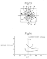
- Fig. 13 Japanese Unexamined Patent Publication No. 5-264957 is illustrated anew based on the direction 12 of the central liquid crystal molecule as in Fig. 1 of the present invention.
- the liquid crystal elements shown in Figs. 1 and 13 are both a STN liquid crystal element having a twist angle of 240° and have an equal ⁇ nd value of 0.78 ⁇ m.
- the absorption axes (8a, 9a) of the upper and lower polarizing plates intersect with each other at an angle of 54°, and the absorption axis 9a of the upper polarizing plate intersects with the alignment direction 7b of the upper liquid crystal molecule at an angle of 39°, while the absorption axis 8a of the lower polarizing plate intersects with the alignment direction 7a of the lower liquid crystal molecule at an angle of 45°.
- the retardation value of the lag axis 13b of the retardation film is a very large 0.6 ⁇ m, and the lag axis 13b of the retardation film is arranged at a position inclined about -28° clockwise from the direction 12 of the central liquid crystal molecule, the absorption axis 9a of the upper polarizing plate forming an angle of 49° with the delay axis 13b of the retardation film.
- the birefringence index assumes a maximum value when the delay axis of the polarizing plate is 45° with respect to the optical compensator and the liquid crystal molecules.
- the absorption axes of the polarizing plates are arranged at a position displaced by 35° to 50° from the alignment directions (7a, 7b) of the upper and lower liquid crystal molecules and the delay axis 13b of the retardation film.
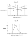
- Fig. 5 is a graph for comparing the voltage vs. transmittance curve representing the change in transmittance with respect to the applied voltage of the liquid crystal shutter between the present invention and the prior art (the curves 20, 21 represent the prior art, and the curve 22 the present invention).
- the dotted curve 20 in the drawing is a voltage vs. transmittance curve of the liquid crystal shutter disclosed in Japanese Unexamined Patent Publication No. 9-119219 using the birefringence for white and the cancellation of the optical rotatory power for black, i.e. a liquid crystal shutter having the relative positions shown in Fig. 11 described above.
- the solid curve 22, shows a voltage vs. transmittance curve of the liquid crystal shutter having the relative positions of Fig. 1 according to the present invention.
- the voltage vs. transmittance curve of the conventional STN liquid crystal display apparatus having the relative positions shown in Fig. 13 is indicated by the one-dot chain 21.
- the liquid crystal shutter disclosed in Japanese Unexamined Patent Publication No. 9-119219 indicated by the curve 20 is such that the transmittance increases temporarily at a voltage of about 2 V and reaching a maximum transmittance Ym, decreases gradually subsequently.
- the liquid crystal shutter according to the present invention shown by the curve 22, on the other hand, is such that superior black is obtained at a voltage of not less than 6 V, a contrast of not less than 100 is obtained at 10 V, and thus a perfect black can be obtained at a lower voltage than in the liquid crystal shutter disclosed in Japanese Unexamined Patent Publication No. 9-119219.
- an optical compensator or a retardation film having a very small retardation film of 0.03 ⁇ m is arranged in such a direction as to subtract the slight remaining birefringence characteristic.
- the birefringence characteristic can be successfully removed even with a drive voltage as low as 10 V, thereby realizing a still higher contrast.
- the response time from the open to the closed state depends on the applied voltage, and is shorter the higher the applied voltage.
- An applied voltage of not less than 10 V can shorten the response time to not more than 1 ms.
- the response time for the transfer from the closed to the open state, which utilizes the elastic effect, on the other hand, depends on the liquid crystal material and the twist angle and, in the case of a material low in viscosity, is shorter the larger the twist angle. With the liquid crystal shutter according to this invention using a twist angle of 180° to 260°, a response time of about 1 ms is possible.
- the maximum transmittance on the curve 21 of the conventional liquid crystal display apparatus is lower than the maximum transmittance Ym of the present invention and undergoes a sharp change for black display at about 2 V, but a perfect black cannot be obtained.
- the contrast value is low.
- a further increase in voltage increases the black level gradually, and therefore the response time from open to closed state cannot be shortened by applying a high voltage.
- the birefringence is utilized for both white display and black display and is adjusted to obtain black and white with small coloring. As a result, it can be driven with 2 to 3 V. Nevertheless, the retardation value of 0.5 to 0.6 ⁇ m is required for the retardation film, and the response speed is as low as several tens of ms. Further, the contrast is as low as not more than 10. Therefore, the conventional liquid crystal display apparatus is not suitably used as a liquid crystal shutter.
- the retardation value of the retardation film is set to 0.1 to 0.15 ⁇ m which is larger than the retardation value of the retardation film or the optical compensator according to the present invention.
- the angle formed between the absorption axis of the lower polarizing plate to the direction of the central liquid crystal molecule is set to -15°, which is greatly different from the figure of 40° to 60° with which the present invention is configured. Therefore, this conventional liquid crystal display apparatus cannot be expected to exhibit an effect equivalent to the contrast and response speed according to the present invention.
- the liquid crystal shutter according to the present invention uses a liquid crystal element having a twist angle of 180° to 260°, and utilizes the birefringence in the open state for white display, while a retardation film having a very small retardation value is arranged in the direction of the central liquid crystal molecule in the closed state for black display. In this way, the slight amount of birefringence remaining, with the liquid crystal molecules standing perpendicular to the substrates is corrected to completely eliminate the birefringence.
- the angle at which the polarizing plates are arranged or the retardation value of the optical compensator or the retardation film are optimized as a liquid crystal shutter, thereby making it possible to provide a liquid crystal shutter having a high contrast and a high-speed response with a drive voltage as low as about 10 V.
- Fig. 15 is a plan view showing the relative positions of polarizing plates and optical compensators of a liquid crystal shutter according to the present invention.
- the liquid crystal shutter according to this embodiment has a structure shown in Fig. 4 (an example of the second aspect) and Fig. 17 (another example of the second aspect), and is configured with a liquid crystal element 14, optical compensators 15, 16 having a front retardation value of 0.03 ⁇ m, an upper polarizing plate 9 and a lower polarizing plate 8, in which the absorption axes of the upper and lower polarizing plates orthogonally intersect with each other.
- Fig. 4 an example of the second aspect
- Fig. 17 another example of the second aspect
- the absorption axis 8a of the lower polarizing plate is arranged at 45° counterclockwise with respect to the direction 12 of the central liquid crystal molecule, and the discotic film is oriented in the direction 13c in such a manner as to intersect orthogonally with the direction 12 of the central liquid crystal molecule.
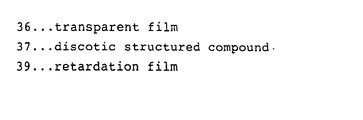
- Fig. 20 is a schematic diagram for explaining the configuration of the discotic film 13 making up an optical compensator.
- the discotic film 13 is produced by coating an alignment layer on a transparent film 36 of triacetyl cellulose (TAC) or the like, rubbing along the alignment direction 13c (See Fig. 15) and then coating a discotic structured compounds 37 (37a 37b, 37c) such as a discotic liquid crystal, followed by orientation and fixing.
- the discotic structured compound 37a on the boundary with the transparent film 36 is aligned substantially in parallel to the transparent film 36, but the other discotic structured compounds have a progressively changing inclination angle along the thickness.
- the discotic structured compound 37c farthest from the transparent film 36 is inclined by 50° to 70° with respect to the alignment direction 13c.
- the discotic structured compound 37a in the neighborhood of the boundary with the transparent film 36, of which the refractive index nx along X axis and the refractive index ny along Y axis are equal to each other for the light incident from the front of the transparent film, has substantially no retardation value.
- the refractive index in the direction orthogonal to the direction 13c of orientation is larger than the refractive index in other directions, which direction corresponds to the delay axis 13a of the optical compensator.
- the retardation value depends on the inclined state of the discotic structured compound 37. Normally, however, the front retardation value is in the range of 0.03 to 0.05 ⁇ m. Further, when the normal optical compensator is inclined in the direction of the extension axis thereof, the retardation value changes in all directions.
- the optical compensator under consideration has the retardation value increased for the light entering from the direction inclined along the arrow indicating the alignment direction 13c, while the retardation value is decreased for the light entering from the direction inclined opposite to the arrow indicating the alignment direction 13c.
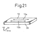
- Fig. 21 is a schematic diagram for explaining the configuration of the retardation film used as an optical compensator.
- the retardation film 39 is an extension film composed of a transparent film 38 of polycarbonate (PC), polyvinyl alcohol (PVA) or polymethyl methacrylate (PMMA) extended along X axis and Y axis.
- PC polycarbonate
- PVA polyvinyl alcohol
- PMMA polymethyl methacrylate
- extension along X axis aligns the polymer molecules in the direction of extension, i.e. along X axis so that the refractive index nx increases beyond the refractive index ny, and the direction nx constitutes the, delay axis.
- extension along X axis increases the refractive index ny as compared with the refractive index nx, so that the direction ny constitutes the delay axis.
- the retardation value of these retardation films on the front is expressed by the equation (nx - ny) x d where d is the thickness of the retardation film.
- d is the thickness of the retardation film.
- a retardation film as thick as 50 to 100 ⁇ m is used.
- Fig. 18 is a plan view for explaining the relative positions in the conventional liquid crystal display apparatus using a single discotic film.
- This liquid crystal display apparatus is configured with, from top to bottom, an upper polarizing plate, a discotic film, a liquid crystal element having a twist angle of 90° and a lower polarizing plate.
- the arrows in the alignment direction 7b of the upper liquid crystal molecule and the alignment direction 7a of the lower liquid crystal molecule indicate the directions of rubbing.
- the liquid crystals on the arrow sides are inclined outward of the substrates.
- this liquid crystal element assumes a structure having a twist angle of 90° with the direction 12 of the central liquid crystal molecule as a priority angle of field (main direction of visual angle) of the liquid crystal display apparatus.
- the absorption axis 9a of the upper polarizing plate is arranged parallel to the alignment direction 7b of the upper liquid crystal molecule, while the absorption axis 8a of the lower polarizing plate is arranged parallel to the alignment direction 7a of the lower liquid crystal molecule thereby to minimize the occurrence of birefringence.
- the discotic film also has an inclination, and therefore the arrow is shown only on one side.
- the portion of the discotic structured compound 37 on the side thereof opposite to the arrow is inclined outward of the transparent film 36.
- the alignment direction 13c of the discotic film 13 is arranged parallel to the alignment direction 12 of the central liquid crystal molecule, as shown in Fig. 18.
- the discotic film constituting an optical compensator is arranged with the alignment direction 13c thereof orthogonal to the direction 12 of the central liquid crystal molecule.
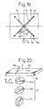
- Fig. 19 is a plan view for explaining the relative positions in the conventional liquid crystal display apparatus using two discotic films.
- This liquid crystal display apparatus is configured with, from top to bottom, an upper polarizing plate, a second discotic film, a liquid crystal element having a twist angle of 90°, a first discotic film and a lower polarizing plate.
- the absorption axis 9a of the upper polarizing plate is arranged parallel to the alignment direction 7b of the upper liquid crystal molecule, while the absorption axis 8a of the lower polarizing plate is arranged parallel to the alignment direction 7a of the lower liquid crystal molecule.
- the alignment direction 16c of the retardation film is arranged parallel to the alignment direction 7b of the upper liquid crystal molecule, while the alignment direction 15c of the retardation film is arranged parallel to the alignment direction 7a of the lower liquid crystal molecule.
- the absorption axis 9a of the upper polarizing plate intersects with the alignment direction 16c of the second discotic film at an angle of 0°, and therefore no retardation is generated by the second discotic film for the light entering from the front.
- the absorption axis 8a of the lower polarizing plate intersects with the alignment direction 15c of the first discotic film also at an angle of 0°, and therefore no retardation is generated.
- the birefringence of the liquid crystal molecules is corrected by generating a retardation, and therefore the operation is different from that of the discotic film according to the prior art.
- the effect of improving the angle of field characteristic of the discotic film according to the prior art is significant for the TN liquid crystal element, and an embodiment for the liquid crystal element having a twist angle of 180° to 260° is not disclosed.
- the liquid crystal element having a twist angle of 180° to 260° is used and the birefringence is utilized in open state for white display.
- the discotic film using a discotic structured compound is arranged orthogonal to the direction of the central liquid crystal molecule, so that the slight remaining birefringence is corrected with the liquid crystal molecules erected perpendicular to the substrates thereby to completely eliminate the birefringence.
- the angle at which the polarizing plates are arranged and the retardation value of the optical compensator are optimized for the liquid crystal shutter, thereby making it possible to provide a liquid crystal shutter which has a high contrast and a high response speed even when driven with a voltage as low as about 10 V.
- Fig. 2 is a sectional view showing the structure of a liquid crystal shutter according to the first embodiment of the invention
- Fig. 1 a plan view as taken from above in Fig. 2.
- the configuration of the liquid crystal shutter according to this invention will be explained below with reference to Figs. 1 and 2.
- This embodiment refers to the case where a single retardation film is used as an optical compensator.
- the liquid crystal shutter according to the first embodiment is configured with a lower polarizing plate 8 arranged under the liquid crystal element 11 having a twist angle of 240°, a retardation film 13 constituting an optical compensator arranged above the liquid crystal element 11, and an upper polarizing plate 9.
- the liquid crystal element 11 is formed of a first substrate 1 of glass 0.7 mm thick formed with a first electrode 2 of ITO making up a transparent electrode and an alignment layer 3 formed thereon, a second substrate 4 of glass 0.7 mm thick with a second electrode 5 of ITO and an alignment layer 6 formed thereon, and a nematic liquid crystal 7.
- the birefringence index ⁇ n of the nematic liquid crystal used is 0.195, and the gap between the first substrate 1 and the second substrate 4 is 4 ⁇ m.
- the value ⁇ nd indicating the birefringence characteristic of the liquid crystal element is set to 0.78 ⁇ m.
- the alignment layer 3 of the first substrate 1 is rubbed along the alignment direction 7a of the lower liquid crystal molecule shown in Fig. 1, and the alignment layer 6 of the second substrate 4 is rubbed along the alignment direction 7b of the upper liquid crystal molecule.
- the lower polarizing plate 8 and the upper polarizing plate 9 are arranged on the two sides, respectively, of the liquid crystal element 11.
- the absorption axis 8a of the lower polarizing plate is arranged at an angle of 45° counterclockwise with respect to the alignment direction 12 of the central liquid crystal molecule indicating the alignment direction of the liquid crystal at the intermediate portion between the first substrate 1 and the second substrate 4 of the nematic liquid crystal 7, while the absorption axis 9a of the upper polarizing plate is arranged at an angle of 45° clockwise with respect to the direction 12 of the central liquid crystal molecule, thus constituting a liquid crystal shutter of positive type assuming an open state when no voltage is applied thereto.
- the retardation film 13 making up an optical compensator has the delay axis 13a (or 13b in the case of the retardation film) thereof arranged parallel to the alignment direction 12 of the central liquid crystal molecule and has a retardation value of 0.03 ⁇ m.
- the retardation film 13 is bonded integrally with the upper polarizing plate 9 by use of an acrylic adhesive.
- a retardation film having such a very small retardation value as described above is difficult to produce.
- a biaxial extension film with a polycarbonate film extended in two directions along X and Y axes is used, and one of the two axial directions having a larger retardation value is defined as an extension axis.
- the linear polarized light that has entered by way of the lower polarizing plate 8 is changed to an elliptical polarized light by the birefringence characteristic of the liquid crystal, thereby leading to an open state in which the light is emitted from the upper polarizing plate 9 as a slightly yellowish white display in what is called a positive display.
- a DC or AC voltage is applied, the liquid crystal molecules stand perpendicular to the substrate, the birefringence is eliminated, and the linear polarized light that has entered by way of the lower polarizing plate 8 proceeds directly through the liquid crystal element and is blocked by the upper polarizing plate.
- a closed state for a black display is assumed.
- the transmittance gradually increases from the initial transmittance Y0 with no voltage applied, and after reaching the maximum transmittance Ym at the applied voltage of about 2 V, falls. Substantially, black is achieved at the applied voltage of 6 V, and the transmittance at the applied voltage of 10 V decreases to below 1/100 of the initial transmittance YO, thus attaining the contrast of not less than 100.
- the retardation film 13 By arranging the retardation film 13 at a position 90° displaced from the horizontal axis providing the average alignment direction of liquid crystal, therefore, the remaining birefringence characteristic can be eliminated. Specifically, the contrast at a low drive voltage can be improved by locating the delay axis of the retardation film 13 at a position parallel to the direction 12 of the central liquid crystal molecule.
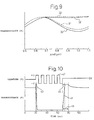
- Fig. 6 is a graph showing the relation between the retardation value of the retardation film 13 and the contrast with a constant voltage applied to the liquid crystal shutter according to the first embodiment.
- a dotted curve 23 represents the case in which the applied voltage is 20 V
- a solid curve 24 the case in which the applied voltage is 10 V
- a one-dot chain curve 25 the case in which the applied voltage is 5 V.
- a contrast of 50 or more is obtained even with the retardation value of zero.
- the contrast of not less than 100 can be obtained, however, by providing a retardation film having a retardation value of 0.03 ⁇ m. With a further increase in retardation value, however, the retardation of the retardation film increases beyond the remaining birefringence so that the contrast rather decreases.
- the contrast is not more than 30 for the retardation value of zero.
- a retardation film having a retardation value of about 0.03 ⁇ m however, a contrast of not less than 100 can be obtained.
- the retardation value of the retardation film 13 is in the range of 0.01 to 0.06 ⁇ m, which improves the contrast more than when the retardation film is lacking.
- the contrast is improved more than when the optical compensator is lacking even with the retardation value of 0.1 ⁇ m.
- the retardation value of the retardation film is applicable within the range of 0.01 to 0.1 ⁇ m although the optimum range thereof varies with the drive voltage.
- Fig. 7 shows the transmittance of a liquid crystal shutter and the angle at which the lower polarizing plate is arranged in the case where the lower polarizing plate 8 is rotated counterclockwise from the direction of the central liquid crystal molecule with the angle of intersection between the absorption axis 8a of the lower polarizing plate 8a and the absorption axis 9a of the upper polarizing plate fixed at 90°, the liquid crystal shutter comprising a liquid crystal element having a twist angle of 240°, an ⁇ nd value of 0.78 ⁇ m and a retardation film having a retardation value of 0.03 ⁇ m.
- the solid curve 28 represents the relation between the maximum transmittance Ym of the liquid crystal shutter according to this invention and the angle at which the polarizing plates are arranged
- the solid curve 29 represents the relation between the angle at which the polarizing plates are arranged and the initial transmittance Y0 with no voltage applied.
- the dotted curve 26 represents the value Ym of the liquid crystal shutter having no retardation film disclosed in Japanese Unexamined Patent Publication No. 9-119219
- the dotted curve 27 represents the value Y0 of a liquid crystal shutter having no retardation film.
- the alignment direction 7a of the lower liquid crystal molecule and the absorption axis 8a of the lower polarizing plate are parallel to each other.
- the initial transmittance Y0 and the maximum transmittance Ym both assume a local maximum value with a small coloring most desirably when the angle at which the lower polarizing plate is arranged is -45° and +45°.
- the angle at which the lower polarizing plate is arranged which can secure the maximum transmittance is somewhat shifted and desirably in the range of -30° to -50° or 40° to 60°. Since the upper polarizing plate is orthogonal, the absorption axis 9a of the upper polarizing plate is also desirably at an angle in the range of 40° to 60° or -30° to -50°.
- Fig. 8 is a graph showing the relation between the angle at which the absorption axes of the upper and lower polarizing plates intersect with each other and the contrast.
- the upper and lower polarizing plates are relocated equally from the position shown in Fig. 1.
- the highest contrast is obtained in the case where the absorption axes of the upper and lower polarizing plates intersect with each other at an angle of 90°.
- the color with no voltage application is also important and, for adjusting the color, it is effective to reduce to about 85° the angle at which the absorption axes of the upper and lower polarizing plates intersect with each other.
- the angle at which the polarizing plates intersect with each other is applicable in the range of 80° to 100°, or preferably in the range of 85° to 95°.
- Fig. 9 shows the transmittance of the liquid crystal shutter and the value ⁇ nd of the liquid crystal element 11 having a twist angle of 240°, with the absorption axis 8a of the lower polarizing plate turned 45° counterclockwise from the direction 12 of the central liquid crystal molecule, and with the absorption axis 8a of the lower polarizing plate and the absorption axis 9a of the upper polarizing plate intersecting with each other at 90°.
- the solid curve 32 represents the maximum transmittance Ym of the liquid crystal shutter according to the invention comprising the retardation film 13 having a retardation value of 0.03 ⁇ m
- the solid curve 33 represents the initial transmittance Y0 with no voltage applied.
- the maximum transmittance Ym of the liquid crystal shutter having no retardation film and the initial transmittance Y0 of the liquid crystal shutter having no retardation film disclosed in Japanese Unexamined Patent Publication No. 9-119219 are shown by the curves 30 and 31, respectively.
- the initial transmittance Y0 with no voltage applied gradually decreases, as shown by the curve 31. An excessively large ⁇ nd, therefore, is not desirable.
- the maximum transmittance Ym also undesirably decreases.
- the delay axis 13a of the compensator 13 (the delay axis 13b of the retardation film) is arranged parallel to the direction 12 of the central liquid crystal molecule, the retardation is added with no voltage applied, so that the white becomes somewhat yellowish.
- the white color can be improved, therefore, by reducing the value ⁇ nd of the liquid crystal element 11 to a value about 0.02 to 0.05 ⁇ m smaller than the value ⁇ nd of the liquid crystal element 10 of the liquid crystal shutter having no retardation film.
- the value ⁇ nd for the liquid crystal element 11 according to this invention is preferably set in the range of 0.6 ⁇ m to 0.9 ⁇ m, or more preferably in the range of 0.65 ⁇ m to 0.8 ⁇ m.
- the optimum ⁇ nd value though somewhat dependent on the twist angle of the liquid crystal element 11 or the retardation value of the retardation film 13, is substantially in the range of 0.6 to 0.9 ⁇ m for the twist angle of 180° to 260°.
- the value ⁇ nd is set to 0.78 ⁇ m for the twist angle 240° of the liquid crystal element 11, and the retardation value of the retardation film 13 is set to 0.03 ⁇ m. In this way, a bright open state for white display with a comparatively small coloring and a contrast of not less than 100 are obtained when a drive voltage of 10 V is applied.
- Fig. 10 shows a drive waveform 42 with an AC signal of 100 Hz, 10 V applied for 50 ms to the liquid crystal shutter according to the present invention, and a transmittance vs. time curve (41) indicating the change in transmittance with time.
- the on response time 43 from the open to the closed state is affected by the applied voltage, and becomes shorter the higher the voltage applied to the liquid crystal shutter.
- the liquid crystal shutter according to the first embodiment is impressed with a voltage of 10 V, and therefore the on response time is very short and less than 1 ms.
- the maximum transmittance is reached within about 1.5 ms, after which the initial transmittance is restored within about 20 ms.
- the off response time from the closed to the open state which uses the elasticity for restoring the twist of the liquid crystal is shorter for the liquid crystal element having a larger twist angle.
- the response time for the liquid crystal element is originally defined as the time required before the change in the liquid crystal molecules is settled and is 20 ms in Fig. 10. In an application as a liquid crystal shutter, however, the time required before restoring the maximum transmittance is effective as a response time, and therefore the off response time 44 of the liquid crystal shutter according to this invention having a twist angle of 240° is 1.5 ms. Thus, a liquid crystal shutter of high response speed is obtained.
- a video printer for writing data in a Polaroid film was test produced using the liquid crystal shutter according to this invention. Even when driven with a low voltage of 10 V, a superior contrast and gradation display were made possible, thereby producing a full-color image print of high quality.
- the retardation film 13 having a retardation value of 0.01 to 0.1 ⁇ m, the liquid crystal element 11 having a twist angle of 180° to 260° and the lower polarizing plate 8 in this way, a liquid crystal shutter high in contrast and response speed even with a low drive voltage of 10 V or less can be provided.
- liquid crystal element 11 having a twist angle of 240° used in the first embodiment
- the use of a liquid crystal element having a twist not less than 180° to 260° in twist angle can produce a similar effect.
- a basically similar effect is obtained also for a twist angle of 270° or more although it is difficult to orient the liquid crystal stably.
- a biaxial extension of the polycarbonate film in X and Y directions is used as a retardation film 13. Nevertheless, a normal uniaxial extension of a retardation film can alternatively be used although a small retardation value cannot be adjusted easily. Further, it is also possible to use a retardation film of a Z type extended along Z axis.
- the retardation film 13 can alternatively be arranged between the liquid crystal element 11 and the lower polarizing plate 8 with exactly the same effect.
- liquid crystal shutter according to the second embodiment of the present invention is configured differently from the first embodiment in that two retardation films 2 are used as an optical compensator (Refer to Figs. 4, and 15, 16 of Fig. 17; the configuration of Fig. 17 will be described in detail later with reference to the fourth embodiment), and the angle at which the upper and lower polarizing plates are arranged and the twist pitch P of the nematic liquid crystal are different.
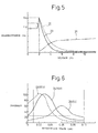
- Fig. 4 is a sectional view showing the structure of a liquid crystal shutter according to the second embodiment of the invention
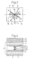
- Fig. 3 is a plan view taken from above in Fig. 4.
- the configuration of the liquid crystal shutter according to the present invention will be explained below with reference to Figs. 3 and 4.
- the liquid crystal shutter according to the second embodiment is configured with a lower polarizing plate 8 arranged under a liquid crystal element 14 having a twist angle of 240°, and a first retardation film 15, a second retardation film 16 and an upper polarizing plate 9 arranged above the liquid crystal element 14.
- the liquid crystal element 14 is formed of a first substrate 1 of glass 0.7 mm thick having a first electrode 2 of ITO and an alignment layer 3 formed thereon, a second substrate 4 of glass 0.7 mm thick having a second electrode 5 of ITO and an alignment layer 6 formed thereon, and a nematic liquid crystal 7.
- the birefringence index ⁇ n of the nematic liquid crystal used is 0.195, and the gap d between the first substrate 1 and the second substrate 4 is 4 ⁇ m. Therefore, the ⁇ nd value indicating the birefringence index of the liquid crystal element is set to 0.78 ⁇ m.
- the alignment layer 3 of the first substrate 1 is rubbed along the alignment direction 7a of the lower liquid crystal molecule in Fig. 3, while the alignment layer 6 of the second substrate 4 is rubbed along the alignment direction 7b of the upper liquid crystal molecule.
- the lower polarizing plate 8 and the upper polarizing plate 9 are arranged on the two sides, respectively, of the liquid crystal element 14.
- the absorption axis 8a of the lower polarizing plate is arranged at a counterclockwise angle of 55° to the direction 12 of the central liquid crystal molecule indicating the alignment direction of the liquid crystal at the intermediate portion between the first substrate 1 and the second substrate 4 of the nematic liquid crystal 7, while the absorption axis 9a of the upper polarizing plate is arranged at an angle of 35° clockwise to the direction 12 of the central liquid crystal molecule, thereby forming a liquid crystal shutter of a positive type.
- the first retardation film 15 is arranged in such a direction that the lag axis 15b is orthogonal to the direction 12 of the central liquid crystal molecule and has a retardation value of 0.15 ⁇ m.
- the second retardation film 16 has the delay axis 16b thereof arranged parallel to the direction 12 of the central liquid crystal molecule and has a retardation value of 0.18 ⁇ m.
- Both retardation films are a transparent film 50 ⁇ m thick having a uniaxial extension of polycarbonate integrated by bonding with the upper polarizing plate 9 using an acrylic adhesive.
- the first embodiment it is generally difficult to produce a retardation film having a very small retardation value of about 0.03 to 0.05 ⁇ m by an ordinary uniaxial extension method.
- the first embodiment therefore, uses a retardation film produced by the more expensive biaxial extension method.
- the second embodiment uses two retardation films each having a small retardation value of 0.03 ⁇ m to 0.05 ⁇ m formed by the inexpensive ordinary uniaxial extension method.
- the delay axis 15b of the first retardation film and the delay axis 16b of the second retardation film are arranged in orthogonal relation as shown in Fig. 3, the actual retardation value is provided by difference between the retardation values of the two retardation films.
- the second retardation film 16 is set to a retardation value 0.03 ⁇ m larger than the first retardation film 15, and therefore substantially the same effect is obtained as if a retardation film having a retardation value of 0.03 ⁇ m is arranged on the lag axis 16b of the second retardation film.
- a high contrast can be obtained even with a low drive voltage.
- the maximum transmittance Ym with a voltage applied for a liquid crystal shutter having no retardation film, as shown by the curve 26 in Fig. 7, can be obtained in the case where the angle at which the lower polarizing plate is arranged corresponds to the position of 45° from the direction 12 of the central liquid crystal molecule.
- the liquid crystal shutter according to this invention comprising a retardation film having a retardation value of 0.03 ⁇ m, however, the maximum transmittance is obtained in the case where the angle at which the lower polarizing plate is arranged corresponds to the position of 55° from the direction 12 of the central liquid crystal molecule.
- the upper and lower polarizing plates are arranged by being rotated 10° counterclockwise from the position of the liquid crystal shutter according to the first embodiment.
- Fig. 14 is a graph showing the relation between d/P which is a quotient between the twist pitch P of the liquid crystal and the gap d between the first substrate 1 and the second substrate 6 on the one hand and the response time at room temperature on the other hand.
- a solid curve 46 represents the on response time with a voltage of 10 V applied, and a solid curve 47 represents the off response time with a voltage of 0 V.
- the on response time 46 increases, though not greatly, with the increase in d/P in view of the fact that the viscosity of the liquid crystal increases with the decrease in twist pitch, while the off response time 47 decreases as the return elasticity is strengthened with the increase in d/P.
- the value d/P of the STN liquid crystal display apparatus is often set in the range of 0.45 to 0.5. It has been ascertained experimentally, however, that since the applied voltage of the liquid crystal shutter according to this invention is 10 V or more which is several times as large as the operation starting voltage, the orientation defect is not caused even with a d/P value larger than 0.5.
- the off response time 47 can be shortened by setting d/P to a large value within a range which does not increase the delay of the on response time considerably.
- the twist angle is ⁇
- d/P is set in the range of 0.65 to ⁇ /360.
- the off response time of the liquid crystal shutter according to the second embodiment can be shortened to 1.2 ms, i.e. to about 80 % of the off response time of the liquid crystal shutter according to the first embodiment.
- the apparatus can be used as a liquid crystal shutter, although the off response time becomes longer.
- the minimum value of d/P is determined from ( ⁇ -90)/360, which is 0.42 for the twist angle of 240°, and 0.25 for the twist angle of 180°. Considering the alignment stability, however, a figure of not less than 0.4 is desirable.
- the range of d/P applicable for a liquid crystal shutter is given as 0.4 ⁇ d/P ⁇ ( ⁇ + 90)/360, the most desirable range being given as 0.5 ⁇ d/P ⁇ ⁇ /360.
- a liquid crystal shutter capable of producing a high contrast even when driven with a low voltage of not more than 10 V can be provided by using the upper polarizing plate 9, the second retardation film 16, the first retardation film 15, the liquid crystal element 14 having a twist angle of 180° to 260° and the lower polarizing plate 8. Further, by optimizing the angle at which the polarizing plates are arranged and setting the twist pitch in the range of 0.5 ⁇ d/P ⁇ ⁇ /360, a liquid crystal shutter which can produce a bright open state with a superior white display and a short response time can be provided.
- the second embodiment uses a liquid crystal element 14 having a twist angle of 240°. Nevertheless, a similar effect can be attained by using a liquid crystal element having a twist not less than the twist angle of 180° to 260°. Also, a similar effect can be obtained basically for a twist angle of not less than 270° in which case the liquid crystal cannot be oriented stably.
- the second retardation film 16 can alternatively be arranged under the first retardation film 15 with equal effect.
- first retardation film 15 and the second retardation film 16 are arranged above the liquid crystal element 14 according to the second embodiment, both the first retardation film 15 and the second retardation film 16 can alternatively be arranged under the liquid crystal element 14.
- the first retardation film 15 and the second retardation film 16 are arranged in two successive layers above the liquid crystal element 14, it is alternatively possible to arrange them separately from each other, that is to say, the first retardation film 15 is arranged under the liquid crystal element 14 and the second retardation film 16 above the liquid crystal element 14, or the first retardation film 15 is arranged above the liquid crystal element 14 and the second retardation film 16 under the liquid crystal element 14.
- a liquid crystal shutter was test produced which was configured with, from top to bottom, the upper polarizing plate 9, the second retardation film 16, the liquid crystal element 14, the first retardation film 15 and the lower polarizing plate 8, which liquid crystal shutter had a superior characteristic similar to the liquid crystal shutter according to the second embodiment.
- the absorption axis 8a of the lower polarizing plate is arranged at 55° counterclockwise with respect to the direction 12 of the central liquid crystal molecule. Nevertheless, a similar effect can be achieved, in spite of the resulting small change in the angle of field characteristic, by rotating the axis 8a by 90° and arranging the absorption axis 9a of the upper polarizing plate at 55° counterclockwise with respect to the direction 12 of the central liquid crystal molecule.
- substantially superior contrast and brightness characteristics can be obtained within the range of 40° to 60°.
- the difference between the retardation value of the second retardation film 16 and the retardation value of the first retardation film 15 is set to 0.03 ⁇ m.
- a similar effect is obtained by setting the difference between the retardation value of the second retardation film 16 and the retardation value of the first retardation film 15 in the range of 0.01 to 0.1 ⁇ m.
- the absolute value of the retardation film used is not specifically limited as long as the difference of the retardation values is in the range of 0.01 to 0.1 ⁇ m.
- Fig. 2 described above is a sectional view applicable also to the structure of the liquid crystal shutter according to the third embodiment
- Fig. 15 is a plan view taken from above in Fig. 2.
- the third embodiment refers to the case where a single discotic film is used as an optical compensator 13.
- the alignment layer 3 of the first substrate 1 is rubbed along the arrow in the direction 7a of orientation of the lower liquid crystal molecule also in Fig. 15, and the alignment layer 6 of the second substrate 4 is rubbed along the arrow in the alignment direction 7b of the upper liquid crystal molecule.
- the liquid crystal molecules are aligned along the alignment direction 7b of the upper liquid crystal molecule and the alignment direction 7a of the lower liquid crystal molecule, and the liquid crystal molecules on the arrow side are inclined outward of the substrates.
- the alignment direction 13c of the discotic film 13 making up an optical compensator is orthogonal to the direction 12 of the central liquid crystal molecule according to the third embodiment.
- Wide View (trade name) of Fuji Film having a retardation value of 0.03 ⁇ m against the light incident from the front was arranged parallel to the horizontal axis h located in the direction of 3 o'clock in Fig. 15.
- the discotic film 13, as shown in Fig. 20, includes discotic structured compounds 37 fixedly aligned in the alignment direction 13c on a transparent film 36 of triacetyl cellulose (TAC) 80 ⁇ m thick.
- TAC triacetyl cellulose
- the direction in which the refractive index becomes maximum against the light entering from the front is orthogonal to the alignment direction 36, and corresponds to the delay axis of an ordinary optical compensator.
- the angle ⁇ formed between the alignment direction 13a of the optical compensator and the absorption axis 9a of the upper polarizing plate is 45° and provides a position most likely to cause a retardation.
- the transparent film 36 of the discotic film 13 and the upper polarizing plate 9 are integrated with each other by an acrylic adhesive, and the discotic structured compound is also coated with the acrylic adhesive and bonded with the liquid crystal element 11.
- the great majority of the liquid crystal molecules stand upright perpendicular to the substrate, while the liquid crystal molecules on the boundary of the substrates are parallel to the substrates and slightly retain a birefringence characteristic.
- the molecules on the boundary surface of the substrates are oriented in the alignment direction 7a of the upper liquid crystal molecule and in the alignment direction 7b of the lower liquid crystal molecule in Fig. 15, and on the average, are arranged orthogonal to the direction 12 of the central liquid crystal molecule, i.e. in the direction parallel to the horizontal axis h in Fig. 15.
- the alignment direction 13c of the discotic film is arranged along the direction of the horizontal axis providing the average alignment direction of the liquid crystal.
- substantially the same situation is achieved as if an optical compensator having a retardation value of 0.03 ⁇ m is arranged parallel to the direction 12 of the central liquid crystal molecule, thus the remaining birefringence characteristic can be completely eliminated.
- the contrast with a low drive voltage can be improved by arranging the alignment direction 13c of the discotic film 13 at a position orthogonal to the direction 12 of the central liquid crystal molecule.
- Fig. 6 shows the relation between the retardation value and the contrast for the light incident from the front with the varying inclination angle of the discotic structured compounds 37 of the discotic film 13 while a constant voltage is applied to the liquid crystal shutter according to this embodiment.
- the dotted curve 23 refers to the case in which the applied voltage is 20 V
- the solid curve 24 to the case where the applied voltage is 10 V
- the one-dot chain curve 25 to the case where the applied voltage is 5 V.
- Fig. 8 described above is a graph indicating the relation between the contrast and the angle at which the absorption axes of the upper and lower polarizing plates intersect with each other.
- the upper and lower polarizing plates were relocated equally from the position shown in Fig. 15.
- the highest contrast could be obtained in the case where the absorption axes of the upper and lower polarizing plates intersect with each other at 90°.
- the color with no voltage applied is important, and the color can be adjusted effectively by reducing the angle at which the absorption axes of the upper and lower polarizing plates intersect with each other to about 85°.
- the angle at which the polarizing plates intersection with other is reduced to 80° or less or increased up to 100° or more, a perfect black cannot be obtained and the contrast is reduced.
- the applicable angle at which the polarizing plates intersect with each other therefore, is in the range of 80° to 100° or preferably in the range of 85° to 95°
- the retardation is added and the white color becomes somewhat yellowish when no voltage is applied. Therefore, the white color can be improved by reducing the value ⁇ nd of the liquid crystal element 11 by about 0.02 to 0.05 ⁇ m from the ⁇ nd value for the liquid crystal element 10 of the liquid crystal shutter having no optical compensator.
- the ⁇ nd value recommended for the liquid crystal element 11 according to this invention is in the range of 0.6 ⁇ m to 0.9 ⁇ m, or especially, the range of 0.65 ⁇ m to 0.8 ⁇ m is preferable.
- the most optimum ⁇ nd value, though somewhat dependent on the twist angle of the liquid crystal element 11 and the retardation value of the discotic film 13, is included substantially in the range of 0.6 to 0.9 ⁇ m for the twist angle of 180° to 260°.
- the on response time 43 is very short and was less than 1 ms while the off response time 44 was 1.5 ms, thereby making it possible to produce a liquid crystal shutter with a high response speed.
- a superior gradation display is obtained, and as described above, a gradation display and a superior contrast are attained even with a low voltage of 10 V in a similar video printer to the one described above, thereby making it possible to produce a full-color image print of high image quality.
- the use of a discotic structured compound film (discotic film) as an optical compensator stabilizes the very small retardation value of the optical compensator, thereby making it possible to provide a liquid crystal shutter with small variations of characteristics.
- the direction 13c of orientation of the discotic film 13 is arranged in the direction of 3 o'clock on the horizontal axis h. Nevertheless, a similar effect can be obtained by arranging the alignment direction 13c in the direction of 9 o'clock on the horizontal axis h, though accompanied it is by a somewhat different angle of field characteristic.
- the discotic film 13 can be arranged between the liquid crystal element 11 and the lower polarizing plate 8 instead of between the liquid crystal element 11 and the upper polarizing plate 9 with quite the same effect.
- two discotic films 13 may be used in two successive layers in the same direction, or one discotic film 13 may be arranged between the liquid crystal element 11 and the upper polarizing plate 9 and the other discotic film 13 between the liquid crystal element 11 and the lower polarizing plate 8 in the same direction.
- the configuration and effects of the liquid crystal shutter according to a fourth embodiment of the present invention will be explained with reference to the drawings.
- the configuration of the liquid crystal shutter according to the fourth embodiment is different from that of the aforementioned embodiments in that two optical compensators are used like in the second embodiment and the twist pitch P of the nematic liquid crystal assumes a different value.
- two discotic films are used as optical compensators.
- Fig. 17 is a sectional view showing the structure of the liquid crystal shutter according to the fourth embodiment of the invention, and Fig. 16 a plan view taken from above in Fig. 17.
- the configuration of the liquid crystal shutter according to this invention will be explained with alternate reference to Figs. 16 and 17.
- the liquid crystal shutter according to the fourth embodiment is configured with a first discotic film 15 and a lower polarizing plate 8 arranged under the liquid crystal element 14 having a twist angle of 240°, and a second discotic film 16 and an upper polarizing plate 9 arranged above the liquid crystal element 11.
- the liquid crystal element 14 is formed of a first substrate 1 of glass 0.7 mm thick with a first electrode 2 of ITO and an alignment layer 3 formed thereon, a second substrate 4 of glass 0.7 mm thick with a second electrode 5 of ITO and an alignment layer 6 formed thereon, and a nematic liquid crystal element 7.
- the birefringence index ⁇ n of the nematic liquid crystal used is 0.195, and the gap d between the first substrate 1 and the second substrate 4 is 4 ⁇ m.
- the ⁇ nd value indicating the birefringence characteristic as a liquid crystal element 14, therefore, is set to 0.78 ⁇ m.
- the alignment layer 3 of the first substrate 1 is rubbed along the arrow in the alignment direction 7a of the lower liquid crystal molecule in Fig. 16, while the alignment layer 6 of the second substrate 4 is rubbed along the arrow in the alignment direction 7b of the upper liquid crystal molecule.
- the liquid crystal molecules are aligned in the alignment direction 7b of the upper liquid crystal molecule and the alignment direction 7a of the lower liquid crystal molecule, so that the liquid crystal molecules on the arrow side are inclined outward of the substrates.
- the lower polarizing plate 8 and the upper polarizing plate 9 are arranged on the two sides, respectively, of the liquid crystal element 14 in such a manner that the absorption axis 8a of the lower polarizing plate and the absorption axis 9a of the upper polarizing plate are orthogonal to each other.
- the absorption axis 8a of the lower polarizing plate is arranged at an angle of 45° counterclockwise with respect to the direction 12 of the central liquid crystal molecule indicating the alignment direction of liquid crystal at the intermediate portion between the first substrate 1 and the second substrate 4 of the nematic liquid crystal 7, while the absorption axis 9a of the upper polarizing plate is arranged at an angle of 45° clockwise with respect to the direction of the central liquid crystal molecule, thereby making up a liquid crystal shutter of positive type.
- the first discotic film 15 has the alignment direction 15c thereof arranged at 20° counterclockwise from the horizontal axis h, and has a front retardation value of 0.03 ⁇ m.
- the second discotic film 16 has the alignment direction 16c arranged at 20° clockwise from the horizontal axis h, and has a retardation value of 0.03 ⁇ m.
- Both discotic films are made of the same material as the discotic film 13 used in the third embodiment described above, and include a transparent film 36 and polarizing plates bonded to each other by an acrylic adhesive, with the coating surface of the discotic structured compounds 37 and the liquid crystal element 14 bonded to each other using an acrylic adhesive.
- the alignment direction 13c of the discotic film 13 is arranged parallel to the horizontal axis h.
- the alignment direction of each discotic film is arranged-at 20° rotated in the alignment direction of the liquid crystal molecules on the substrate side associated with the particular discotic film. Specifically, as shown in Fig. 16, the angle formed between the alignment direction 15c of the first discotic film 15 and the horizontal axis h is set to 20°, and the angle formed between the alignment direction 16c of the second discotic film 16 and the horizontal axis h is set to 20°.
- the angle between the alignment direction 15c of the first discotic film 15 and the alignment direction 7a of the lower liquid crystal molecule is 10°, while the angle formed between the alignment direction 15c of the first discotic film 15 and the alignment direction 7b of the upper liquid crystal molecule is not more than 50°.
- the angle formed between the alignment direction 16c of the second discotic film 16 and the alignment direction 7b of the upper liquid crystal molecule is 10°, while the angle between the alignment direction 16c of the second discotic film 16 and the alignment direction 7a of the lower liquid crystal molecule is not more than 50°.
- the remaining birefringence characteristic can be removed most efficiently in the case where the alignment direction of the discotic film is parallel to the horizontal axis h. Nevertheless, the birefringence characteristic can be eliminated up to the angle of 0° to 40° to the horizontal axis h. At the angles of 50° to 90° to the horizontal axis, in contrast, the retardation of the discotic film is added to the residual birefringence characteristic of the liquid crystal element.
- two discotic films having a retardation value of 0.03 ⁇ m are used. In the case where they are both arranged parallel to the horizontal axis h, therefore, the retardation value becomes 0.06 ⁇ m.
- a contrast of only about 20 can be obtained as indicated by the curve 24 in Fig. 6 with a voltage of 10 V.
- the angle at which the discotic films are arranged is changed by about 0° to 30°, and then the total retardation value corrected by the two discotic films is reduced to 0.02 to 0.03 ⁇ m, thereby making it possible to obtain a contrast of not less than 80 with a drive voltage of 10 V.
- the alignment direction 15c of the first discotic film 15 is set to the range of 90° to 120° counterclockwise with respect to the direction 12 of the central liquid crystal molecule, i.e. to the range of 0° to 30° counterclockwise from the horizontal axis h, the alignment direction 15c becomes substantially parallel to the alignment direction 7a of the lower liquid crystal molecule, more desirably resulting in an improved angle of field characteristic.
- the contrast can be improved in the case where the alignment direction 15c of the first discotic film 15 is in the range of 60° to 120° counterclockwise with respect to the direction 12 of the central liquid crystal molecule, and the angle of field characteristic can also be improved in the range of 90° to 120°.
- the alignment direction 16 of the second discotic film 16 is arranged at the angle in the range of 60° to 90° counterclockwise with respect to the direction 12 of the central liquid crystal molecule, i.e. in the range of 0° to 30° clockwise from the horizontal axis h, then the direction 16c substantially becomes parallel to the alignment direction 7b of the upper liquid crystal molecule, more desirably resulting in an improved angle of field characteristic.
- the conventional liquid crystal display apparatus presupposes that the angle formed between the absorption axis 9a of the upper polarizing plate and the alignment direction 16c of the second discotic film 16 is set to the range of 0° or 90° in order to avoid the effect of the retardation on the front of the retardation film, and is considerably different in configuration from the present invention in which the retardation is utilized positively.
- the applied voltage of the liquid crystal shutter is not less than 10 V and is several times larger than the operation start voltage, and it has been experimentally ascertained that even in the case where the d/P value is larger than 0.5, no orientation defect occurs. Further, the off response time for the liquid crystal shutter according to the third embodiment described above could be shortened to about 80 %.
- a field sequential color display apparatus has been test produced with the liquid crystal shutter according to the present invention, in which three types of light-emitting diodes of red, green and blue are sequentially turned on at intervals of 5 ms so that only the desired color is transmitted by use of the liquid crystal shutter for multicolor display.
- a beautiful "color tone" high in contrast can be obtained even with a low drive voltage of 10 V, and also a display with a superior angle of field characteristic could be realized.
- the fourth embodiment of the invention using the upper polarizing plate 9, the second discotic film 16, the liquid crystal element 14 having a twist angle of 180° to 260°, the first discotic film 15 and the lower polarizing plate 8, there is provided a liquid crystal shutter which can produce a high contrast even when driven with a low voltage of not more than 10 V. Further, by optimizing the angle at which the discotic films are arranged, a wide angle of field characteristic is obtained, thereby providing a liquid crystal shutter most suitable for the field sequential color display apparatus.
- the absorption axis 8a of the lower polarizing plate may alternatively be turned by 90° while the absorption axis 9a of the upper polarizing plate is arranged at 45° counterclockwise with respect to the direction 12 of the central liquid crystal molecule to produce a similar effect, though accompanied by some change in the angle of field characteristic.
- the absorption axis 8a of the lower polarizing plate is arranged at 45° counterclockwise with respect to the direction 12 of the central liquid crystal molecule. Nevertheless, a substantially superior contrast and brightness characteristics can be obtained by arranging the absorption axis 8a in the range of 40° to 60°.
- the retardation value of the second discotic film 16 and the retardation value of the first discotic film 15 are set to 0.03 ⁇ m according to the fourth embodiment, a similar effect can be obtained by setting the retardation value of both discotic films in the range of 0.01 ⁇ m to 0.1 ⁇ m, as explained in the third embodiment, even though the optimum range is somewhat varied with the drive voltage.
- a liquid crystal shutter of high brightness and contrast which can be driven with a voltage as low as not more than 10 V and has a high on/off response speed.
- the use of the liquid crystal shutter according to the present invention with a simplified drive circuit can reduce the cost and power consumption, thereby making possible application to portable equipment driven by a battery. Also, since the angle at which the two optical compensators (retardation films or discotic films) are arranged is optimized, a high contrast can be achieved with a low drive voltage like in the aforementioned case, thereby providing a liquid crystal shutter with an even more superior angle of field characteristic. Thus, the present invention has a very great industrial applicability.
Landscapes
- Physics & Mathematics (AREA)
- Nonlinear Science (AREA)
- Chemical & Material Sciences (AREA)
- Crystallography & Structural Chemistry (AREA)
- General Physics & Mathematics (AREA)
- Optics & Photonics (AREA)
- Mathematical Physics (AREA)
- Liquid Crystal (AREA)
Abstract
A liquid crystal shutter of this invention comprises
a liquid crystal element holding a nematic liquid
crystal, of 180° to 260° in twist angle, between a pair
of substrates, a pair of polarizing plates sandwiching
the liquid crystal element, and a retardation film
inserted between the liquid crystal element and one
polarizing plate. The angle formed by the absorption
axes of the polarizing plates is set in the range of 80°
to 100°, the angle formed between the absorption axis of
one of the polarizing plates and the direction of the
central liquid crystal molecule of the liquid crystal
element is set in the range of 40° to 60°, and the delay
axis of the retardation film is arranged substantially
parallel to the alignment direction of the central liquid
crystal molecule of the liquid crystal element. Further,
the retardation film is arranged on a discotic film at an
inclination angle varying along thickness in such a
manner that the alignment direction of the retardation
film is substantially orthogonal to the direction of the
central liquid crystal molecule. Furthermore, the liquid
crystal shutter comprises a first retardation film and a
second retardation which are, for example, aligned on the
retardation film with an inclination angle varying along
the thickness thereof (Fig. 1).
Description
The present invention relates to a liquid crystal
shutter or, in particular, to a liquid shutter in which
the peripheral circuit or especially the drive circuit
can be simplified and the cost and power consumption can
be reduced by realizing a low-voltage drive, a high-speed
shutter on-off response, a high contrast, etc. The
liquid crystal shutter according to this invention has
the various advantages as described above, and therefore
can find application in various fields such as battery-driven
portable equipment, liquid crystal photoprinters
and liquid crystal optical elements.
Conventionally, various liquid crystal shutters have
been proposed. Their performance, however, is not yet
satisfactory, and market demand is high for a liquid
crystal shutter for a liquid crystal printer or a liquid
crystal optical element high in response speed, bright,
high in contrast, drivable by a simple method and capable
of a gradated display.
The liquid crystal shutters under development are
roughly classified, according to the type of the liquid
crystal material used, into (1) a liquid crystal shutter
using an ordinary nematic liquid crystal, (2) a liquid
crystal shutter using a two-frequency drive nematic
liquid crystal having positive or negative dielectric
constant depending on the frequency, and (3) a liquid
crystal shutter using a ferroelectric liquid crystal
having a spontaneous polarization.
The liquid crystal shutter using the ordinary
nematic liquid crystal in (1) above is further divided,
according to the operating principle, into two well-known
types including (a) a TN (twisted nematic) liquid crystal
system in which white or black is displayed by use of the
property of the optical rotatory power rotating the
incident light, and the optical rotatory power is
canceled by applying a voltage to the pixels and erecting
the liquid crystal molecules at an angle substantially
perpendicular to the substrate, and (b) a STN (super
twisted nematic) liquid crystal system using a liquid
crystal element having a twist angle of 180° to 260° in
which black or white is displayed by applying a voltage
to the pixels and thus changing the birefringence which
causes a retardation of the incident light.
The prior art having the configuration described in
(a) above is disclosed in, for example, Japanese
Unexamined Patent Publication No. 62-150330. This
conventional system is configured with a TN liquid
crystal element having a twist angle of 90° and a pair of
polarizing plates arranged on the two sides of the liquid
crystal element in such a manner the absorption axes
thereof are orthogonal to each other.
Another conventional system is disclosed, for
example, in Japanese Unexamined Patent Publication No. 9-113864.
In this prior art, which uses a liquid crystal
element having a twist angle of 270°, polarizing plates
are arranged parallel or perpendicular to the alignment
direction of the upper and lower substrates thereby to
utilize the optical rotatory power.
The conventional system of (b) described above
includes a STN liquid crystal display apparatus called
the yellow mode used as an ordinary liquid crystal
display apparatus. In the conventional system such as
the STN liquid crystal display apparatus having a twist
angle of 240°, for example, the angles of intersection
between the absorption axes of the upper and lower
polarizing plates is about 60°, and the angle between the
alignment direction of the substrates and the absorption
axes of the polarizing plates is set to about 45°.
In the case where the a twist angle of 90° is used
in the system of (a) above, the response time required to
transfer from the open state to the closed state by
applying a voltage is as short as several ms, while the
problem is the slow response time of 10 to several tens
of ms for returning from the closed state to the open
state by removing the voltage. Further, in the case
where the twist of 270° is used, the orientational
stability of the liquid crystal element is difficult to
achieve, which makes it impractically necessary to use an
obliquely vapor deposited SiO film or the like special
alignment layer capable of attaining a high pretilt.
In the system of (b), on the other hand, the use of
a practical STN liquid crystal element having the twist
angle of 225° to 250° can attain a short response time of
several ms for transferring from closed to open state.
In the closed state, however, a voltage is applied to the
liquid crystal element to make a bluish black liquid
crystal with a low contrast of about 10. In addition, a
further increase in applied voltage undesirably increases
the brightness again by changing the elliptical polarized
state. Therefore, the applied voltage cannot be set to a
very high level, with the result that the response time
from open to closed state becomes as long as 10 to
several tens of ms, thereby posing the problem of poor
practicability as a liquid crystal shutter.
Further, based on the aforementioned study of the
prior art, the present inventor has proposed a system
using a liquid crystal element having a twist angle of
180° to 260°, as disclosed in Japanese Unexamined Patent
Publication No. 9-119219, in which the birefringence is
utilized for white display as in the STN liquid crystal
system while the optical rotatory power is canceled for
black display by erecting the liquid crystal molecules
substantially perpendicular to the substrate.
Now, the system proposed by the present inventor
will be explained with reference to Figs. 11 and 12.
Fig. 12 is a sectional view showing the structure of this
liquid crystal shutter, and Fig. 11 is a plan view
showing the alignment direction of liquid crystal
molecules as viewed from the top in Fig. 12. This liquid
crystal shutter, as shown in Fig. 12, has a liquid
crystal element 10 having a twist angle of 240°, a lower
polarizing plate 8 and an upper polarizing plate 9.
The liquid crystal element 10 is formed of a first
substrate 1 of glass 0.7 mm thick with a first electrode
2 of ITO and an alignment layer 3 formed thereon, a
second substrate 4 of glass 0.7 mm thick with a second
electrode 5 of ITO providing a transparent electrode and
an alignment layer 6 formed thereon, and a nematic liquid
crystal 7. The birefringence index Δn of the nematic
liquid crystal 7 used in this case is 0.2, and the gap d
between the first substrate 1 and the second substrate 4
is 4 µm. Therefore, the value Δnd indicating the
birefringence characteristic of the liquid crystal
element 10 is set to 0.8 µm,
The alignment layer 3 associated with the first
substrate 1 is rubbed in the alignment direction of the
lower liquid crystal molecules located on the boundary
surface of the first substrate 1 arranged on the lower
side, i.e. in the alignment direction 7b (See Fig. 11) of
the lower liquid crystal molecule. The alignment layer 6
of the second substrate 4, on the other hand, is rubbed
in the alignment direction of the upper liquid crystal
molecules located on the boundary surface of the second
substrate 4 located on the upper side, i.e. in the
direction 7a (See Fig. 11) of alignment of the upper
liquid crystal molecule. Further, a substance having an
optically rotatory power called a chiral material is
added to the nematic liquid crystal 7 having a viscosity
of 18 cp, so that the twist pitch P is adjusted to 8 µm
to obtain the relation d/P = 0.5 thereby to form a liquid
crystal element having a counterclockwise twist angle of
240°.
Also, the lower polarizing plate 8 and the upper
polarizing plate 9 are arranged on the two sides,
respectively, of the liquid crystal element 10 in such a
manner that the absorption axis 8a of the lower
polarizing plate and the absorption axis 9a of the upper
polarizing plate are orthogonal to each other. The
absorption axis 8a of the lower polarizing plate is
arranged at an angle of 45° counterclockwise to the
direction 12 of the central liquid crystal molecule
indicating the alignment direction of liquid crystal at
the intermediate portion between the first substrate 1
and the second substrate 4 of the nematic liquid crystal
7. The absorption axis 9a of the upper polarizing plate,
on the other hand, is arranged at an angle of 45°
clockwise to the direction 12 of alignment of the central
liquid crystal molecule, thereby making up a liquid
crystal shutter of positive type displaying white in the
absence of a voltage applied thereto.
As long as no voltage is applied, the linear
polarized light entering from the lower polarizing plate
8 is changed to an elliptical polarized light by the
birefringence characteristic of the liquid crystal, and,
assuming an open state, emitted as white light colored
slightly yellowish as compared with the upper polarizing
plate 9. Upon application thereto of 20 to 30 V, DC or
AC, the liquid crystal molecules are erected in the
direction perpendicular to the substrates, and lose both
the birefringence characteristic and the optical rotatory
power. Thus, the linear polarized light entering by way
of the lower polarizing plate 8 proceeds directly through
the liquid crystal element and is blocked by the upper
polarizing plate 9, thereby changing to a closed state
for black display.
The liquid crystal shutter of this type uses a
liquid crystal element having a twist angle of 180° to
260°. The response time from closed to open state,
therefore, is 1 to 2 ms and much shorter than that of the
conventional TN liquid crystal shutter having a twist
angle of 90° utilizing the optical rotatory power with
the polarizing plates arranged parallel to the liquid
crystal molecules, thus making possible a high-speed
response. The response time from open to closed state,
on the other hand, is not more than 1 ms upon application
of a high voltage of 20 to 30 V. Further, the absence of
the birefringence characteristic in closed state for
black display produces a high contrast.
The technique disclosed in Japanese Unexamined
Patent Publication No. 9-119219 described above, however,
requires a drive voltage of not less than 20 V, and
therefore uses a drive IC and a boosting circuit with a
high breakdown voltage as a drive circuit.
The object of the present invention is to provide a
liquid crystal shutter, which can be driven with a low
voltage of not higher than 10 V by reducing the drive
voltage thereof further, and in which the on/off
switching of the shutter can be performed at high speed
while at the same time producing a high contrast, on the
one hand, and to reduce the cost and the power
consumption by simplifying the drive circuit using the
particular liquid crystal shutter, on the other hand.
In order to achieve the object described above,
according to a first aspect of the present invention,
there is provided a liquid crystal shutter comprising a
liquid crystal element holding a nematic liquid crystal
having a twist angle of 180° to 260° between a pair of
substrates including a first substrate and a second
substrate, a pair of polarizing plates arranged to hold
the liquid crystal element described above therebetween,
and an optical compensator arranged between the liquid
crystal element and one of the polarizing plates,
characterized in that the angle formed between the absorption axes of the pair of the polarizing plates is set in the range of 80° to 100°, the angle formed by the absorption axis of one of the polarizing plates and the direction of central liquid crystal molecule of the liquid crystal element is set in the range of 40° to 60°, and the delay axis of the optical compensator is arranged substantially in parallel to the direction of the central liquid crystal molecule of the liquid crystal element.
characterized in that the angle formed between the absorption axes of the pair of the polarizing plates is set in the range of 80° to 100°, the angle formed by the absorption axis of one of the polarizing plates and the direction of central liquid crystal molecule of the liquid crystal element is set in the range of 40° to 60°, and the delay axis of the optical compensator is arranged substantially in parallel to the direction of the central liquid crystal molecule of the liquid crystal element.
Also, this aspect of the invention is characterized
in that the retardation value on the front of the optical
compensator is set in the range of 0.01 to 0.1 µm.
Further, this aspect of the invention is
characterized in that the value Δnd which is the product
of the birefringence index Δn of the nematic liquid
crystal and the gap d between the first substrate and the
second substrate is set in the range of 0.6 to 0.9 µm.
Also, this aspect of the invention is characterized
in that the optical compensator is a retardation film and
the lag axis of the optical compensator has the same
direction as the lag axis of the retardation film.
Further, the optical compensator is a discotic film
with a discotic structured compound aligned on a
transparent film at a varying inclination angle along the
thickness thereof, and the delay axis of the optical
compensator is an optical axis orthogonal to the
alignment direction of the discotic film.
An example of a liquid crystal shutter according to
the second aspect of the present invention comprises a
liquid crystal element with a nematic liquid crystal
having a twist angle of 180° to 260° held between a pair
of substrates including a first substrate and a second
substrate, a pair of polarizing plates, a pair of
polarizing plates arranged to hold the liquid crystal
element, and a first optical compensator and a second
optical compensator arranged between the liquid crystal
element and one of the polarizing plates,
characterized in that the angle formed between the absorption axes of the pair of the polarizing plates is set in the range of 80° to 100°, and the angle formed between the absorption axis of said one of the polarizing plates and the alignment direction of the central liquid crystal molecule of the liquid crystal element is set in the range of 40° to 60°.
characterized in that the angle formed between the absorption axes of the pair of the polarizing plates is set in the range of 80° to 100°, and the angle formed between the absorption axis of said one of the polarizing plates and the alignment direction of the central liquid crystal molecule of the liquid crystal element is set in the range of 40° to 60°.
Another example of the liquid crystal shutter
according to the second aspect comprises a liquid crystal
element with a nematic liquid crystal having a twist
angle of 180° to 260° held between a pair of substrates
including a first substrate and a second substrate, a
pair of polarizing plates arranged with the liquid
crystal element held therebetween, a first optical
compensator arranged between the liquid crystal element
and one of the polarizing plates, and a second optical
compensator arranged between the liquid crystal element
and the other polarizing plate,
characterized in that the angles formed between the absorption axes of the pair of the polarizing plates is set in the range of 80° to 100°, and the angle formed between the absorption axis of said one of the polarizing plates and the alignment direction of the central liquid crystal molecule of the liquid crystal element is set in the range of 40° to 60°.
characterized in that the angles formed between the absorption axes of the pair of the polarizing plates is set in the range of 80° to 100°, and the angle formed between the absorption axis of said one of the polarizing plates and the alignment direction of the central liquid crystal molecule of the liquid crystal element is set in the range of 40° to 60°.
Also, this aspect of the invention is characterized
in that the difference between the retardation value on
the front of the first optical compensator and the
retardation value on the front of the second optical
compensator is set in the range of 0.01 to 0.1 µm.
Further, this aspect of the invention is
characterized in that the value Δnd which is the product
of the birefringence index Δn of the nematic liquid
crystal and the gap d between the first substrate and the
second substrate is set in the range of 0.6 to 0.9 µm.
Furthermore, this aspect of the invention is
characterized in that the value d/P which is the quotient
between the twist pitch P of the nematic liquid crystal
of a liquid crystal element having a twist angle of and
the gap d between the first substrate and the second
substrate is set in the range of 0.5 to /360.
Also, this aspect of the invention is characterized
in that the first optical compensator is a first
retardation film, the second optical compensator is a
second retardation film, the delay axis of the first
retardation film is arranged substantially orthogonally
orthogonally to the direction of the central liquid
crystal molecule of the liquid crystal element, and the
delay axis of the second retardation film is arranged
substantially parallel to the direction of the central
liquid crystal molecule of the liquid crystal element.
According to still further aspect of the invention,
there is provided liquid crystal shutter, characterized
in that the first optical compensator and the second
optical compensator are each a discotic film with a
discotic structured compound aligned on a transparent
film at a varying inclination angle along the thickness
thereof, and one of the pair of the polarizing plates
makes up an upper polarizing plate, the other polarizing
plate makes up a lower polarizing plate, the first
optical compensator is a first discotic film, and the
first discotic film is interposed between the lower
polarizing plate and the liquid crystal element,
characterized in that the direction orthogonal to the direction of the central liquid crystal molecule of the liquid crystal element makes up a horizontal axis, the angle formed between the alignment direction of the first discotic film and the horizontal axis is set in the range of 0° to 30 °, the angle formed between the alignment direction of the first discotic film and the alignment direction of the lower liquid crystal molecule is not more than the angle formed between the alignment direction of the first discotic film and the alignment direction of the upper liquid crystal molecule;
characterized in that the direction orthogonal to the direction of the central liquid crystal molecule of the liquid crystal element makes up a horizontal axis, the angle formed between the alignment direction of the first discotic film and the horizontal axis is set in the range of 0° to 30 °, the angle formed between the alignment direction of the first discotic film and the alignment direction of the lower liquid crystal molecule is not more than the angle formed between the alignment direction of the first discotic film and the alignment direction of the upper liquid crystal molecule;
The operation of a liquid crystal shutter according
to the first aspect of the invention (the case in which
one optical compensator is used and corresponding to
claims 1 to 5 and the first and third embodiments) and
the second aspect (the case in which two optical
compensators are used and corresponding to claims 6 to 12
and the second and fourth embodiments) will be explained
in detail below while at the same time explaining the
problem points of the conventional structure, with
reference to the drawings.
In the description that follows, the generic concept
is defined as the optical compensator (13, 15, 16 in the
drawings) and the more limitative concept of the optical
compensator is defined as the retardation film and the
discotic film. The optical compensator has a lag axis
(13a, 15a, 16a) in the same direction as the lag axis
(13b, 15b, 16b) of the retardation film and in the
direction orthogonal to the direction (13c, 15c, 16c) of
orientation of the discotic film.
Fig. 1 is a plan view showing an example of the
relative positions of the polarizing plates, the optical
compensator or the retardation film of a liquid crystal
shutter according to this invention. Also, Fig. 2 is a
diagram showing the structure of an example of a liquid
crystal shutter according to this invention. As shown in
Fig. 2, the liquid crystal shutter comprises a liquid
crystal element 11, an optical compensator (or a
retardation film) having a retardation value of 0.03 µm,
an upper polarizing plate 9 and a lower polarizing plate
8. The absorption axes of the upper and lower polarizing
plates 9, 8 are orthogonal to each other. As shown in
Fig. 1, the absorption axis 8a of the lower polarizing
plate is arranged at an angle of 45° counterclockwise to
the direction 12 of the central liquid crystal molecule,
and the delay axis 13a of the optical compensator (or the
lag axis 13b of the retardation film) is arranged
parallel to the direction 12 of the central liquid
crystal molecule.
Incidentally, in the conventional liquid crystal
display apparatus using a retardation film, the
absorption axes of the polarizing plates are generally
arranged to intersect with each other at an angle of 60°
to 70° in order to secure the birefringence of the liquid
crystal molecules. Japanese Unexamined Patent
Publication No. 5-264957, for example, illustrates a
configuration of a liquid crystal display apparatus using
one retardation film and a liquid crystal display
apparatus using two retardation films. The drawing of
Japanese Unexamined Patent Publication No. 5-264957
configured to have two retardation films shows that the
upper and lower polarizing plates are arranged in such a
manner that the absorption axes thereof intersect with
each other at an angle of 70°. Further, the extension
axes (corresponding to the delay axes according to the
present invention) of the two retardation films intersect
with each other at an angle of 10 °, and each of the two
retardation films is arranged at an angle of 40° to 50°
to the direction of the central liquid crystal molecule.
Also, the configuration of the liquid crystal
display apparatus using one retardation film is
illustrated in Japanese Unexamined Patent Publication No.
5-264957. In order to clarify the difference between
Fig. 1 of the present invention and Japanese Unexamined
Patent Publication No. 5-264957, the latter is shown in
Fig. 13. Specifically, Japanese Unexamined Patent
Publication No. 5-264957 is illustrated anew based on the
direction 12 of the central liquid crystal molecule as in
Fig. 1 of the present invention. The liquid crystal
elements shown in Figs. 1 and 13 are both a STN liquid
crystal element having a twist angle of 240° and have an
equal Δnd value of 0.78 µm.
In Fig. 13, the absorption axes (8a, 9a) of the
upper and lower polarizing plates intersect with each
other at an angle of 54°, and the absorption axis 9a of
the upper polarizing plate intersects with the alignment
direction 7b of the upper liquid crystal molecule at an
angle of 39°, while the absorption axis 8a of the lower
polarizing plate intersects with the alignment direction
7a of the lower liquid crystal molecule at an angle of
45°. Also, the retardation value of the lag axis 13b of
the retardation film is a very large 0.6 µm, and the lag
axis 13b of the retardation film is arranged at a
position inclined about -28° clockwise from the direction
12 of the central liquid crystal molecule, the absorption
axis 9a of the upper polarizing plate forming an angle of
49° with the delay axis 13b of the retardation film.
As described above, in the conventional liquid
crystal display apparatus having a retardation film, the
birefringence index assumes a maximum value when the
delay axis of the polarizing plate is 45° with respect to
the optical compensator and the liquid crystal molecules.
In order to easily secure the birefringence, therefore,
the absorption axes of the polarizing plates are arranged
at a position displaced by 35° to 50° from the alignment
directions (7a, 7b) of the upper and lower liquid crystal
molecules and the delay axis 13b of the retardation film.
Fig. 5 is a graph for comparing the voltage vs.
transmittance curve representing the change in
transmittance with respect to the applied voltage of the
liquid crystal shutter between the present invention and
the prior art (the curves 20, 21 represent the prior art,
and the curve 22 the present invention). The dotted
curve 20 in the drawing is a voltage vs. transmittance
curve of the liquid crystal shutter disclosed in Japanese
Unexamined Patent Publication No. 9-119219 using the
birefringence for white and the cancellation of the
optical rotatory power for black, i.e. a liquid crystal
shutter having the relative positions shown in Fig. 11
described above. The solid curve 22, on the other hand,
shows a voltage vs. transmittance curve of the liquid
crystal shutter having the relative positions of Fig. 1
according to the present invention. For comparison, the
voltage vs. transmittance curve of the conventional STN
liquid crystal display apparatus having the relative
positions shown in Fig. 13 is indicated by the one-dot
chain 21.
As shown, the liquid crystal shutter disclosed in
Japanese Unexamined Patent Publication No. 9-119219
indicated by the curve 20 is such that the transmittance
increases temporarily at a voltage of about 2 V and
reaching a maximum transmittance Ym, decreases gradually
subsequently. The liquid crystal shutter according to
the present invention shown by the curve 22, on the other
hand, is such that superior black is obtained at a
voltage of not less than 6 V, a contrast of not less than
100 is obtained at 10 V, and thus a perfect black can be
obtained at a lower voltage than in the liquid crystal
shutter disclosed in Japanese Unexamined Patent
Publication No. 9-119219.
In the state in which 10 V is applied to the liquid
crystal elements, shown by the curves 20 and 22, almost
all the liquid crystal molecules stand perpendicular to
the substrates, while the liquid crystal molecules in the
boundary between the upper and lower substrates are
parallel to the substrates and considered to be located
in the alignment direction along which the upper and
lower substrates are rubbed. Thus, when 10 V is applied,
birefringence of the liquid crystal element is not
completely eliminated.
In view of this, in the liquid crystal shutter
according to the present invention, an optical
compensator or a retardation film having a very small
retardation film of 0.03 µm is arranged in such a
direction as to subtract the slight remaining
birefringence characteristic. In this way, the
birefringence characteristic can be successfully removed
even with a drive voltage as low as 10 V, thereby
realizing a still higher contrast.
The response time from the open to the closed state
depends on the applied voltage, and is shorter the higher
the applied voltage. An applied voltage of not less than
10 V can shorten the response time to not more than 1 ms.
The response time for the transfer from the closed to the
open state, which utilizes the elastic effect, on the
other hand, depends on the liquid crystal material and
the twist angle and, in the case of a material low in
viscosity, is shorter the larger the twist angle. With
the liquid crystal shutter according to this invention
using a twist angle of 180° to 260°, a response time of
about 1 ms is possible.
On the other hand, the maximum transmittance on the
curve 21 of the conventional liquid crystal display
apparatus is lower than the maximum transmittance Ym of
the present invention and undergoes a sharp change for
black display at about 2 V, but a perfect black cannot be
obtained. As compared with the present invention,
therefore, the contrast value is low. A further increase
in voltage increases the black level gradually, and
therefore the response time from open to closed state
cannot be shortened by applying a high voltage.
Specifically, in the conventional liquid crystal
display apparatus using the retardation film, the
birefringence is utilized for both white display and
black display and is adjusted to obtain black and white
with small coloring. As a result, it can be driven with
2 to 3 V. Nevertheless, the retardation value of 0.5 to
0.6 µm is required for the retardation film, and the
response speed is as low as several tens of ms. Further,
the contrast is as low as not more than 10. Therefore,
the conventional liquid crystal display apparatus is not
suitably used as a liquid crystal shutter.
Another example of the liquid crystal display
apparatus using the retardation film having a retardation
value of 0.1 to 0.15 µm is disclosed in Japanese
Unexamined Patent Publication No. 6-3665. The basic
operation is similar to that of the present invention,
except that an attempt is made to improve the contrast by
compensating for the birefringence remaining in the
liquid crystal element with the retardation film while
the voltage is being applied.
Also with this liquid crystal display apparatus, in
order to drive it with an applied voltage of 2 to 3 V,
the retardation value of the retardation film is set to
0.1 to 0.15 µm which is larger than the retardation value
of the retardation film or the optical compensator
according to the present invention. Also, the angle
formed between the absorption axis of the lower
polarizing plate to the direction of the central liquid
crystal molecule is set to -15°, which is greatly
different from the figure of 40° to 60° with which the
present invention is configured. Therefore, this
conventional liquid crystal display apparatus cannot be
expected to exhibit an effect equivalent to the contrast
and response speed according to the present invention.
In order to obviate the various problem points of
the prior art described above, the liquid crystal shutter
according to the present invention uses a liquid crystal
element having a twist angle of 180° to 260°, and
utilizes the birefringence in the open state for white
display, while a retardation film having a very small
retardation value is arranged in the direction of the
central liquid crystal molecule in the closed state for
black display. In this way, the slight amount of
birefringence remaining, with the liquid crystal
molecules standing perpendicular to the substrates is
corrected to completely eliminate the birefringence.
Further, the angle at which the polarizing plates are
arranged or the retardation value of the optical
compensator or the retardation film are optimized as a
liquid crystal shutter, thereby making it possible to
provide a liquid crystal shutter having a high contrast
and a high-speed response with a drive voltage as low as
about 10 V.
Now, the operation of the liquid crystal shutter
according to the second aspect of the present invention
will be explained in detail with reference to the
drawings. Fig. 15 is a plan view showing the relative
positions of polarizing plates and optical compensators
of a liquid crystal shutter according to the present
invention. In this diagram, the liquid crystal shutter
according to this embodiment has a structure shown in
Fig. 4 (an example of the second aspect) and Fig. 17
(another example of the second aspect), and is configured
with a liquid crystal element 14, optical compensators
15, 16 having a front retardation value of 0.03 µm, an
upper polarizing plate 9 and a lower polarizing plate 8,
in which the absorption axes of the upper and lower
polarizing plates orthogonally intersect with each other.
As shown in Fig. 15, the absorption axis 8a of the lower
polarizing plate is arranged at 45° counterclockwise with
respect to the direction 12 of the central liquid crystal
molecule, and the discotic film is oriented in the
direction 13c in such a manner as to intersect
orthogonally with the direction 12 of the central liquid
crystal molecule.
Fig. 20 is a schematic diagram for explaining the
configuration of the discotic film 13 making up an
optical compensator. The discotic film 13 is produced by
coating an alignment layer on a transparent film 36 of
triacetyl cellulose (TAC) or the like, rubbing along the
alignment direction 13c (See Fig. 15) and then coating a
discotic structured compounds 37 ( 37a 37b, 37c) such as a
discotic liquid crystal, followed by orientation and
fixing. The discotic structured compound 37a on the
boundary with the transparent film 36 is aligned
substantially in parallel to the transparent film 36, but
the other discotic structured compounds have a
progressively changing inclination angle along the
thickness. Thus, the discotic structured compound 37c
farthest from the transparent film 36 is inclined by 50°
to 70° with respect to the alignment direction 13c.
Specifically, the discotic structured compound 37a
in the neighborhood of the boundary with the transparent
film 36, of which the refractive index nx along X axis
and the refractive index ny along Y axis are equal to
each other for the light incident from the front of the
transparent film, has substantially no retardation value.
The discotic structured compound 37c farthest from the
transparent film 36 which is inclined by 50° to 70°, on
the other hand, develops a retardation due to the
anisotropy between the refractive index nz in the
direction along the thickness and the refractive index ny
along the Y axis.
Specifically, the refractive index in the direction
orthogonal to the direction 13c of orientation is larger
than the refractive index in other directions, which
direction corresponds to the delay axis 13a of the
optical compensator. The retardation value depends on
the inclined state of the discotic structured compound
37. Normally, however, the front retardation value is in
the range of 0.03 to 0.05 µm. Further, when the normal
optical compensator is inclined in the direction of the
extension axis thereof, the retardation value changes in
all directions. The optical compensator under
consideration, however, has the retardation value
increased for the light entering from the direction
inclined along the arrow indicating the alignment
direction 13c, while the retardation value is decreased
for the light entering from the direction inclined
opposite to the arrow indicating the alignment direction
13c.
Fig. 21 is a schematic diagram for explaining the
configuration of the retardation film used as an optical
compensator. The retardation film 39 is an extension
film composed of a transparent film 38 of polycarbonate
(PC), polyvinyl alcohol (PVA) or polymethyl methacrylate
(PMMA) extended along X axis and Y axis. In the case of
PC or PVA, extension along X axis aligns the polymer
molecules in the direction of extension, i.e. along X
axis so that the refractive index nx increases beyond the
refractive index ny, and the direction nx constitutes the,
delay axis. In the case of PMMA, on the other hand,
extension along X axis increases the refractive index ny
as compared with the refractive index nx, so that the
direction ny constitutes the delay axis.
The retardation value of these retardation films on
the front is expressed by the equation
(nx - ny) x d
where d is the thickness of the retardation film.
Generally, a retardation film as thick as 50 to 100 µm is
used.
Now, an explanation will be given of a conventional
liquid crystal display apparatus having an optical
compensator using a discotic film. The optical
compensator using a discotic film finds wide applications
for improving the angle of field characteristic of the
liquid crystal display apparatus in TN mode. As an
example, the liquid crystal display apparatus disclosed
in Japanese Unexamined Patent Publication No. 8-50206
will be explained with reference to Figs. 18 and 19.
Fig. 18 is a plan view for explaining the relative
positions in the conventional liquid crystal display
apparatus using a single discotic film. This liquid
crystal display apparatus is configured with, from top to
bottom, an upper polarizing plate, a discotic film, a
liquid crystal element having a twist angle of 90° and a
lower polarizing plate. In Fig. 18, the arrows in the
alignment direction 7b of the upper liquid crystal
molecule and the alignment direction 7a of the lower
liquid crystal molecule indicate the directions of
rubbing. The liquid crystals on the arrow sides are
inclined outward of the substrates.
Thus, this liquid crystal element assumes a
structure having a twist angle of 90° with the direction
12 of the central liquid crystal molecule as a priority
angle of field (main direction of visual angle) of the
liquid crystal display apparatus. The absorption axis 9a
of the upper polarizing plate is arranged parallel to the
alignment direction 7b of the upper liquid crystal
molecule, while the absorption axis 8a of the lower
polarizing plate is arranged parallel to the alignment
direction 7a of the lower liquid crystal molecule thereby
to minimize the occurrence of birefringence.
On the other hand, the discotic film also has an
inclination, and therefore the arrow is shown only on one
side. As shown in Fig. 20, the portion of the discotic
structured compound 37 on the side thereof opposite to
the arrow is inclined outward of the transparent film 36.
In the conventional liquid crystal display apparatus, in
order to improve the angle of field characteristic, the
alignment direction 13c of the discotic film 13 is
arranged parallel to the alignment direction 12 of the
central liquid crystal molecule, as shown in Fig. 18.
In the liquid crystal shutter according to this
invention, however, as shown in Fig. 15, in order to
completely eliminate the birefringence of the liquid
crystal element with a voltage applied thereto, the
discotic film constituting an optical compensator is
arranged with the alignment direction 13c thereof
orthogonal to the direction 12 of the central liquid
crystal molecule. Thus, the operation of the present
invention and that of the prior art are quite different.
Fig. 19 is a plan view for explaining the relative
positions in the conventional liquid crystal display
apparatus using two discotic films. This liquid crystal
display apparatus is configured with, from top to bottom,
an upper polarizing plate, a second discotic film, a
liquid crystal element having a twist angle of 90°, a
first discotic film and a lower polarizing plate. The
absorption axis 9a of the upper polarizing plate is
arranged parallel to the alignment direction 7b of the
upper liquid crystal molecule, while the absorption axis
8a of the lower polarizing plate is arranged parallel to
the alignment direction 7a of the lower liquid crystal
molecule. The alignment direction 16c of the retardation
film is arranged parallel to the alignment direction 7b
of the upper liquid crystal molecule, while the alignment
direction 15c of the retardation film is arranged
parallel to the alignment direction 7a of the lower
liquid crystal molecule.
The absorption axis 9a of the upper polarizing plate
intersects with the alignment direction 16c of the second
discotic film at an angle of 0°, and therefore no
retardation is generated by the second discotic film for
the light entering from the front. In similar fashion,
the absorption axis 8a of the lower polarizing plate
intersects with the alignment direction 15c of the first
discotic film also at an angle of 0°, and therefore no
retardation is generated. According to the present
invention, on the other hand, the birefringence of the
liquid crystal molecules is corrected by generating a
retardation, and therefore the operation is different
from that of the discotic film according to the prior
art. Also, the effect of improving the angle of field
characteristic of the discotic film according to the
prior art is significant for the TN liquid crystal
element, and an embodiment for the liquid crystal element
having a twist angle of 180° to 260° is not disclosed.
With the liquid crystal shutter according to this
invention, therefore, as will be explained with reference
to the third embodiment later, the liquid crystal element
having a twist angle of 180° to 260° is used and the
birefringence is utilized in open state for white
display. In the closed state for black display, on the
other hand, the discotic film using a discotic structured
compound is arranged orthogonal to the direction of the
central liquid crystal molecule, so that the slight
remaining birefringence is corrected with the liquid
crystal molecules erected perpendicular to the substrates
thereby to completely eliminate the birefringence.
Further, the angle at which the polarizing plates are
arranged and the retardation value of the optical
compensator are optimized for the liquid crystal shutter,
thereby making it possible to provide a liquid crystal
shutter which has a high contrast and a high response
speed even when driven with a voltage as low as about 10
V.
Preferred embodiments for implementing the first and
second aspects of the present invention and the effects
thereof will be explained in detail below with reference
to the drawings.
First, the configuration of a liquid crystal shutter
according to the first embodiment of the invention will
be explained with reference to the drawings. Fig. 2 is a
sectional view showing the structure of a liquid crystal
shutter according to the first embodiment of the
invention, and Fig. 1 a plan view as taken from above in
Fig. 2. The configuration of the liquid crystal shutter
according to this invention will be explained below with
reference to Figs. 1 and 2. This embodiment refers to
the case where a single retardation film is used as an
optical compensator.
The liquid crystal shutter according to the first
embodiment is configured with a lower polarizing plate 8
arranged under the liquid crystal element 11 having a
twist angle of 240°, a retardation film 13 constituting
an optical compensator arranged above the liquid crystal
element 11, and an upper polarizing plate 9. The liquid
crystal element 11 is formed of a first substrate 1 of
glass 0.7 mm thick formed with a first electrode 2 of ITO
making up a transparent electrode and an alignment layer
3 formed thereon, a second substrate 4 of glass 0.7 mm
thick with a second electrode 5 of ITO and an alignment
layer 6 formed thereon, and a nematic liquid crystal 7.
The birefringence index Δn of the nematic liquid crystal
used is 0.195, and the gap between the first substrate 1
and the second substrate 4 is 4 µm. The value Δnd
indicating the birefringence characteristic of the liquid
crystal element is set to 0.78 µm.
The alignment layer 3 of the first substrate 1 is
rubbed along the alignment direction 7a of the lower
liquid crystal molecule shown in Fig. 1, and the
alignment layer 6 of the second substrate 4 is rubbed
along the alignment direction 7b of the upper liquid
crystal molecule. Also, the nematic liquid crystal
having a viscosity of 18 cp has added thereto a material
having an optical rotatory power called a chiral
material, with the twist pitch P thereof adjusted to 8 µm
so that the relation d/P = 0.5 is secured, thereby
forming a liquid crystal element having a
counterclockwise twist angle of 240°.
In order that the absorption axis 8a of the lower
polarizing plate and the absorption axis 9a of the upper
polarizing plate may intersect with each other
orthogonally, the lower polarizing plate 8 and the upper
polarizing plate 9 are arranged on the two sides,
respectively, of the liquid crystal element 11. The
absorption axis 8a of the lower polarizing plate is
arranged at an angle of 45° counterclockwise with respect
to the alignment direction 12 of the central liquid
crystal molecule indicating the alignment direction of
the liquid crystal at the intermediate portion between
the first substrate 1 and the second substrate 4 of the
nematic liquid crystal 7, while the absorption axis 9a of
the upper polarizing plate is arranged at an angle of 45°
clockwise with respect to the direction 12 of the central
liquid crystal molecule, thus constituting a liquid
crystal shutter of positive type assuming an open state
when no voltage is applied thereto.
The retardation film 13 making up an optical
compensator has the delay axis 13a (or 13b in the case of
the retardation film) thereof arranged parallel to the
alignment direction 12 of the central liquid crystal
molecule and has a retardation value of 0.03 µm. The
retardation film 13 is bonded integrally with the upper
polarizing plate 9 by use of an acrylic adhesive. With
an ordinary uniaxial extension method, a retardation film
having such a very small retardation value as described
above is difficult to produce. According to the first
embodiment, a biaxial extension film with a polycarbonate
film extended in two directions along X and Y axes is
used, and one of the two axial directions having a larger
retardation value is defined as an extension axis.
Now, the effects of the liquid crystal shutter
according to the first embodiment will be explained. The
change in transmittance upon application of an AC voltage
of 300 Hz in frequency to the liquid crystal shutter of
this configuration is indicated by a solid curve 22 shown
in Fig. 5 as described above.
As long as no voltage is applied, on the other hand,
the linear polarized light that has entered by way of the
lower polarizing plate 8 is changed to an elliptical
polarized light by the birefringence characteristic of
the liquid crystal, thereby leading to an open state in
which the light is emitted from the upper polarizing
plate 9 as a slightly yellowish white display in what is
called a positive display. When a DC or AC voltage is
applied, the liquid crystal molecules stand perpendicular
to the substrate, the birefringence is eliminated, and
the linear polarized light that has entered by way of the
lower polarizing plate 8 proceeds directly through the
liquid crystal element and is blocked by the upper
polarizing plate. Thus a closed state for a black
display is assumed.
As shown by the curve 22 in Fig. 5, in the liquid
crystal shutter according to the first embodiment, the
transmittance gradually increases from the initial
transmittance Y0 with no voltage applied, and after
reaching the maximum transmittance Ym at the applied
voltage of about 2 V, falls. Substantially, black is
achieved at the applied voltage of 6 V, and the
transmittance at the applied voltage of 10 V decreases to
below 1/100 of the initial transmittance YO, thus
attaining the contrast of not less than 100.
Specifically, with a voltage of 10 V applied to the
liquid crystal element 11, almost all the liquid crystal
molecules stand perpendicular to the substrates while the
liquid crystal molecules on the boundary of the
substrates are parallel to the substrates and retain the
birefringence characteristic slightly. Then, the
molecules on the boundary surface of the substrates are
oriented along the alignment direction 7a of the upper
liquid crystal molecule and the alignment direction 7b of
the lower liquid crystal molecule in Fig. 1. On the
average, they assume a direction orthogonal to the
alignment direction 12 of the central liquid crystal
molecule and are aligned in the direction parallel to the
horizontal axis in Fig. 1.
By arranging the retardation film 13 at a position
90° displaced from the horizontal axis providing the
average alignment direction of liquid crystal, therefore,
the remaining birefringence characteristic can be
eliminated. Specifically, the contrast at a low drive
voltage can be improved by locating the delay axis of the
retardation film 13 at a position parallel to the
direction 12 of the central liquid crystal molecule.
Now, the retardation value of the retardation film
13 will be explained. Fig. 6 is a graph showing the
relation between the retardation value of the retardation
film 13 and the contrast with a constant voltage applied
to the liquid crystal shutter according to the first
embodiment. A dotted curve 23 represents the case in
which the applied voltage is 20 V, a solid curve 24 the
case in which the applied voltage is 10 V, and a one-dot
chain curve 25 the case in which the applied voltage is 5
V.
In the case where the applied voltage is 20 V, as
indicated by the curve 23, a contrast of 50 or more is
obtained even with the retardation value of zero. The
contrast of not less than 100 can be obtained, however,
by providing a retardation film having a retardation
value of 0.03 µm. With a further increase in retardation
value, however, the retardation of the retardation film
increases beyond the remaining birefringence so that the
contrast rather decreases.
In the case where the applied voltage is 10 V, on
the other hand, as indicated by the curve 24, the
contrast is not more than 30 for the retardation value of
zero. By using a retardation film having a retardation
value of about 0.03 µm, however, a contrast of not less
than 100 can be obtained. Also, the retardation value of
the retardation film 13 is in the range of 0.01 to 0.06
µm, which improves the contrast more than when the
retardation film is lacking.
With a further decrease of the applied voltage to 5
V, as indicated by the curve 25, the contrast is improved
more than when the optical compensator is lacking even
with the retardation value of 0.1 µm. In this way, the
retardation value of the retardation film is applicable
within the range of 0.01 to 0.1 µm although the optimum
range thereof varies with the drive voltage.
Now, the relative positions of the polarizing plates
will be explained. Fig. 7 shows the transmittance of a
liquid crystal shutter and the angle at which the lower
polarizing plate is arranged in the case where the lower
polarizing plate 8 is rotated counterclockwise from the
direction of the central liquid crystal molecule with the
angle of intersection between the absorption axis 8a of
the lower polarizing plate 8a and the absorption axis 9a
of the upper polarizing plate fixed at 90°, the liquid
crystal shutter comprising a liquid crystal element
having a twist angle of 240°, an Δnd value of 0.78 µm and
a retardation film having a retardation value of 0.03 µm.
The solid curve 28 represents the relation between
the maximum transmittance Ym of the liquid crystal
shutter according to this invention and the angle at
which the polarizing plates are arranged, and the solid
curve 29 represents the relation between the angle at
which the polarizing plates are arranged and the initial
transmittance Y0 with no voltage applied. For
comparison, the dotted curve 26 represents the value Ym
of the liquid crystal shutter having no retardation film
disclosed in Japanese Unexamined Patent Publication No.
9-119219, and the dotted curve 27 represents the value Y0
of a liquid crystal shutter having no retardation film.
With the polarizing plates arranged at an angle of
-60°, the alignment direction 7a of the lower liquid
crystal molecule and the absorption axis 8a of the lower
polarizing plate are parallel to each other. With the
liquid crystal shutter having no retardation film, on the
other hand, as indicated by the curves 26 and 27, the
initial transmittance Y0 and the maximum transmittance Ym
both assume a local maximum value with a small coloring
most desirably when the angle at which the lower
polarizing plate is arranged is -45° and +45°.
With the liquid crystal shutter according to this
invention comprising a retardation film having a
retardation value of 0.03 µm, in contrast, the angle at
which the lower polarizing plate is arranged which can
secure the maximum transmittance is somewhat shifted and
desirably in the range of -30° to -50° or 40° to 60°.
Since the upper polarizing plate is orthogonal, the
absorption axis 9a of the upper polarizing plate is also
desirably at an angle in the range of 40° to 60° or -30°
to -50°.
Fig. 8 is a graph showing the relation between the
angle at which the absorption axes of the upper and lower
polarizing plates intersect with each other and the
contrast. The upper and lower polarizing plates are
relocated equally from the position shown in Fig. 1. As
indicated by the curve 35, the highest contrast is
obtained in the case where the absorption axes of the
upper and lower polarizing plates intersect with each
other at an angle of 90°.
In the case where the liquid crystal shutter
according to this invention is used with a field
sequential color display apparatus having a light source
of a plurality of colors, the color with no voltage
application is also important and, for adjusting the
color, it is effective to reduce to about 85° the angle
at which the absorption axes of the upper and lower
polarizing plates intersect with each other. As
indicated by the curve 35, however, in the case where the
angle of intersection is reduced to 80° or less or
increased to 100° or more, a perfect black cannot be
obtained due to a reduced contrast. Therefore, the angle
at which the polarizing plates intersect with each other
is applicable in the range of 80° to 100°, or preferably
in the range of 85° to 95°.
Now, the value Δnd of the liquid crystal element 11
will be explained. Fig. 9 shows the transmittance of the
liquid crystal shutter and the value Δnd of the liquid
crystal element 11 having a twist angle of 240°, with the
absorption axis 8a of the lower polarizing plate turned
45° counterclockwise from the direction 12 of the central
liquid crystal molecule, and with the absorption axis 8a
of the lower polarizing plate and the absorption axis 9a
of the upper polarizing plate intersecting with each
other at 90°. In the diagram, the solid curve 32
represents the maximum transmittance Ym of the liquid
crystal shutter according to the invention comprising the
retardation film 13 having a retardation value of 0.03
µm, and the solid curve 33 represents the initial
transmittance Y0 with no voltage applied. For
comparison, the maximum transmittance Ym of the liquid
crystal shutter having no retardation film and the
initial transmittance Y0 of the liquid crystal shutter
having no retardation film disclosed in Japanese
Unexamined Patent Publication No. 9-119219 are shown by
the curves 30 and 31, respectively.
With the liquid crystal shutter having no
retardation film, as indicated by the curve 30, the
maximum transmittance Ym assumes a maximum value at Δnd
= 0.65 µm and remains substantially unchanged with a
further increase in Δnd. The initial transmittance Y0
with no voltage applied, on the other hand, gradually
decreases, as shown by the curve 31. An excessively
large Δnd, therefore, is not desirable. With the
decrease of Δnd to less than 0.65 µm, on the other hand,
the maximum transmittance Ym also undesirably decreases.
With the liquid crystal shutter according this
invention comprising a retardation film 13 having a
retardation value of 0.03 µm, the value Δnd associated
with the maximum transmittance is somewhat shifted so
that the maximum transmittance Ym is reached at Δnd =
0.67 µm. The initial transmittance Y0 also assumes a
maximum value at Δnd = 0.67 µm, and gradually decreases
with a further increase in Δnd, as indicated by the
curve 33.
In the case where the delay axis 13a of the
compensator 13 (the delay axis 13b of the retardation
film) is arranged parallel to the direction 12 of the
central liquid crystal molecule, the retardation is added
with no voltage applied, so that the white becomes
somewhat yellowish. The white color can be improved,
therefore, by reducing the value Δnd of the liquid
crystal element 11 to a value about 0.02 to 0.05 µm
smaller than the value Δnd of the liquid crystal element
10 of the liquid crystal shutter having no retardation
film.
The value Δnd for the liquid crystal element 11
according to this invention is preferably set in the
range of 0.6 µm to 0.9 µm, or more preferably in the
range of 0.65 µm to 0.8 µm. The optimum Δnd value,
though somewhat dependent on the twist angle of the
liquid crystal element 11 or the retardation value of the
retardation film 13, is substantially in the range of 0.6
to 0.9 µm for the twist angle of 180° to 260°.
According to the first embodiment, the value Δnd is
set to 0.78 µm for the twist angle 240° of the liquid
crystal element 11, and the retardation value of the
retardation film 13 is set to 0.03 µm. In this way, a
bright open state for white display with a comparatively
small coloring and a contrast of not less than 100 are
obtained when a drive voltage of 10 V is applied.
Now, the response time of the liquid crystal shutter
according to this invention will be explained. Fig. 10
shows a drive waveform 42 with an AC signal of 100 Hz, 10
V applied for 50 ms to the liquid crystal shutter
according to the present invention, and a transmittance
vs. time curve (41) indicating the change in
transmittance with time. Upon application of an AC
signal in the open state without any voltage applied, the
transmittance increases for a moment, followed by
blackening into closed state. The on response time 43
from the open to the closed state is affected by the
applied voltage, and becomes shorter the higher the
voltage applied to the liquid crystal shutter. The
liquid crystal shutter according to the first embodiment
is impressed with a voltage of 10 V, and therefore the on
response time is very short and less than 1 ms.
When the AC signal is returned to 0 V from the
closed state, on the other hand, the maximum
transmittance is reached within about 1.5 ms, after which
the initial transmittance is restored within about 20 ms.
The off response time from the closed to the open state
which uses the elasticity for restoring the twist of the
liquid crystal is shorter for the liquid crystal element
having a larger twist angle. The response time for the
liquid crystal element is originally defined as the time
required before the change in the liquid crystal
molecules is settled and is 20 ms in Fig. 10. In an
application as a liquid crystal shutter, however, the
time required before restoring the maximum transmittance
is effective as a response time, and therefore the off
response time 44 of the liquid crystal shutter according
to this invention having a twist angle of 240° is 1.5 ms.
Thus, a liquid crystal shutter of high response speed is
obtained.
Before the maximum transmittance is reached in the
open state from black in closed state, a somewhat bluish
white is displayed with a comparatively small coloring.
After the lapse of about 10 ms which is a holding time
(designated by 45) during which the maximum transmittance
is maintained, the transmittance is reduced with a
somewhat yellowish coloring. As a result, for a gradated
display, a reset signal is applied to restore the closed
state within the holding time 45 when the liquid crystal
shutter maintains the maximum transmittance, and the
state with a small coloring between the closed state and
the maximum transmittance is utilized, thereby making
possible a superior gradation display with high
brightness.
A video printer for writing data in a Polaroid film
was test produced using the liquid crystal shutter
according to this invention. Even when driven with a low
voltage of 10 V, a superior contrast and gradation
display were made possible, thereby producing a full-color
image print of high quality.
As described above, by using the upper polarizing
plate 9, the retardation film 13 having a retardation
value of 0.01 to 0.1 µm, the liquid crystal element 11
having a twist angle of 180° to 260° and the lower
polarizing plate 8 in this way, a liquid crystal shutter
high in contrast and response speed even with a low drive
voltage of 10 V or less can be provided.
Instead of the liquid crystal element 11 having a
twist angle of 240° used in the first embodiment, the use
of a liquid crystal element having a twist not less than
180° to 260° in twist angle can produce a similar effect.
A basically similar effect is obtained also for a twist
angle of 270° or more although it is difficult to orient
the liquid crystal stably.
Also, according to the first embodiment, a biaxial
extension of the polycarbonate film in X and Y directions
is used as a retardation film 13. Nevertheless, a normal
uniaxial extension of a retardation film can
alternatively be used although a small retardation value
cannot be adjusted easily. Further, it is also possible
to use a retardation film of a Z type extended along Z
axis.
Further, unlike the first embodiment in which the
retardation film 13 is arranged between the liquid
crystal element 11 and the upper polarizing plate 9, the
retardation film 13 can alternatively be arranged between
the liquid crystal element 11 and the lower polarizing
plate 8 with exactly the same effect.
The effects of a liquid crystal shutter according to
the second embodiment of the present invention will be
explained with reference to the drawings. The liquid
crystal shutter according to the second embodiment is
configured differently from the first embodiment in that
two retardation films 2 are used as an optical
compensator (Refer to Figs. 4, and 15, 16 of Fig. 17; the
configuration of Fig. 17 will be described in detail
later with reference to the fourth embodiment), and the
angle at which the upper and lower polarizing plates are
arranged and the twist pitch P of the nematic liquid
crystal are different.
The configuration of the liquid crystal shutter
according to the second embodiment of the present
invention will be explained with reference to the
drawings. Fig. 4 is a sectional view showing the
structure of a liquid crystal shutter according to the
second embodiment of the invention, and Fig. 3 is a plan
view taken from above in Fig. 4. The configuration of
the liquid crystal shutter according to the present
invention will be explained below with reference to Figs.
3 and 4.
The liquid crystal shutter according to the second
embodiment is configured with a lower polarizing plate 8
arranged under a liquid crystal element 14 having a twist
angle of 240°, and a first retardation film 15, a second
retardation film 16 and an upper polarizing plate 9
arranged above the liquid crystal element 14. The liquid
crystal element 14 is formed of a first substrate 1 of
glass 0.7 mm thick having a first electrode 2 of ITO and
an alignment layer 3 formed thereon, a second substrate 4
of glass 0.7 mm thick having a second electrode 5 of ITO
and an alignment layer 6 formed thereon, and a nematic
liquid crystal 7.
The birefringence index Δn of the nematic liquid
crystal used is 0.195, and the gap d between the first
substrate 1 and the second substrate 4 is 4 µm.
Therefore, the Δnd value indicating the birefringence
index of the liquid crystal element is set to 0.78 µm.
The alignment layer 3 of the first substrate 1 is
rubbed along the alignment direction 7a of the lower
liquid crystal molecule in Fig. 3, while the alignment
layer 6 of the second substrate 4 is rubbed along the
alignment direction 7b of the upper liquid crystal
molecule. The nematic liquid crystal having a viscosity
of 18 cp has added thereto a substance, having an optical
rotatory power, called a chiral material, with the twist
pitch P adjusted to 6.15 µm to obtain the relation d/P =
0.65, thereby forming a liquid crystal element having a
twist angle of 240° counterclockwise.
In order that the absorption axis 8a of the lower
polarizing plate and the absorption axis 9a of the upper
polarizing plate intersect with each other orthogonally,
the lower polarizing plate 8 and the upper polarizing
plate 9 are arranged on the two sides, respectively, of
the liquid crystal element 14. The absorption axis 8a of
the lower polarizing plate is arranged at a
counterclockwise angle of 55° to the direction 12 of the
central liquid crystal molecule indicating the alignment
direction of the liquid crystal at the intermediate
portion between the first substrate 1 and the second
substrate 4 of the nematic liquid crystal 7, while the
absorption axis 9a of the upper polarizing plate is
arranged at an angle of 35° clockwise to the direction 12
of the central liquid crystal molecule, thereby forming a
liquid crystal shutter of a positive type.
The first retardation film 15 is arranged in such a
direction that the lag axis 15b is orthogonal to the
direction 12 of the central liquid crystal molecule and
has a retardation value of 0.15 µm. The second
retardation film 16, on the other hand, has the delay
axis 16b thereof arranged parallel to the direction 12 of
the central liquid crystal molecule and has a retardation
value of 0.18 µm. Both retardation films are a
transparent film 50 µm thick having a uniaxial extension
of polycarbonate integrated by bonding with the upper
polarizing plate 9 using an acrylic adhesive.
Now, the effects of the second embodiment will be
explained. First, the effects of using two retardation
films will be described. As explained in the first
embodiment, it is generally difficult to produce a
retardation film having a very small retardation value of
about 0.03 to 0.05 µm by an ordinary uniaxial extension
method. The first embodiment, therefore, uses a
retardation film produced by the more expensive biaxial
extension method. The second embodiment, on the other
hand, uses two retardation films each having a small
retardation value of 0.03 µm to 0.05 µm formed by the
inexpensive ordinary uniaxial extension method.
Specifically, in the case where the delay axis 15b of the
first retardation film and the delay axis 16b of the
second retardation film are arranged in orthogonal
relation as shown in Fig. 3, the actual retardation value
is provided by difference between the retardation values
of the two retardation films.
According to the second embodiment, the second
retardation film 16 is set to a retardation value 0.03 µm
larger than the first retardation film 15, and therefore
substantially the same effect is obtained as if a
retardation film having a retardation value of 0.03 µm is
arranged on the lag axis 16b of the second retardation
film. Thus, like the effects of the first embodiment, a
high contrast can be obtained even with a low drive
voltage.
Now, the relative positions of the polarizing plates
will be explained. As explained in the first embodiment,
the maximum transmittance Ym with a voltage applied for a
liquid crystal shutter having no retardation film, as
shown by the curve 26 in Fig. 7, can be obtained in the
case where the angle at which the lower polarizing plate
is arranged corresponds to the position of 45° from the
direction 12 of the central liquid crystal molecule.
With the liquid crystal shutter according to this
invention comprising a retardation film having a
retardation value of 0.03 µm, however, the maximum
transmittance is obtained in the case where the angle at
which the lower polarizing plate is arranged corresponds
to the position of 55° from the direction 12 of the
central liquid crystal molecule. As shown in Fig. 3,
therefore, the upper and lower polarizing plates are
arranged by being rotated 10° counterclockwise from the
position of the liquid crystal shutter according to the
first embodiment.
By thus arranging the upper and lower polarizing
plates by rotating them by 10°, respectively, though the
color with no voltage applied is somewhat yellowish, the
brightness at the maximum transmittance Ym with a voltage
applied has increased and a superior white color can be
obtained.
Now, the relation between the twist pitch of the
liquid crystal and the response time will be explained.
Fig. 14 is a graph showing the relation between d/P which
is a quotient between the twist pitch P of the liquid
crystal and the gap d between the first substrate 1 and
the second substrate 6 on the one hand and the response
time at room temperature on the other hand. A solid
curve 46 represents the on response time with a voltage
of 10 V applied, and a solid curve 47 represents the off
response time with a voltage of 0 V. The on response
time 46 increases, though not greatly, with the increase
in d/P in view of the fact that the viscosity of the
liquid crystal increases with the decrease in twist
pitch, while the off response time 47 decreases as the
return elasticity is strengthened with the increase in
d/P.
In an ordinary STN liquid crystal display apparatus
having a twist angle of 240°, depending on the tilt angle
of the alignment layer used, an increase in the d/P value
beyond 0.5 causes an orientation defect called the stripe
domain and deteriorates the display quality extremely
upon application of a voltage almost equal to the
operation start voltage of about 2 V. Thus, the value
d/P of the STN liquid crystal display apparatus is often
set in the range of 0.45 to 0.5. It has been ascertained
experimentally, however, that since the applied voltage
of the liquid crystal shutter according to this invention
is 10 V or more which is several times as large as the
operation starting voltage, the orientation defect is not
caused even with a d/P value larger than 0.5.
As a result, the off response time 47 can be
shortened by setting d/P to a large value within a range
which does not increase the delay of the on response time
considerably. If the twist angle is , the desired twist
angle is obtained up to the value of d/P = ( + 90)/360,
and beyond that, the twist angle is the desired twist
angle plus 180°. Specifically, in the case where the
desired twist angle is 240°, the actual twist angle is
240° up to d/P = 0.91, and 420° beyond that.
According to the second embodiment, in order not to
increase the on response time excessively, d/P is set in
the range of 0.65 to /360. In this way, the off
response time of the liquid crystal shutter according to
the second embodiment can be shortened to 1.2 ms, i.e. to
about 80 % of the off response time of the liquid crystal
shutter according to the first embodiment.
Of course, even when the value of d/P is set to not
more than 0.5, the apparatus can be used as a liquid
crystal shutter, although the off response time becomes
longer. The minimum value of d/P is determined from (-90)/360,
which is 0.42 for the twist angle of 240°, and
0.25 for the twist angle of 180°. Considering the
alignment stability, however, a figure of not less than
0.4 is desirable. Thus, the range of d/P applicable for
a liquid crystal shutter is given as 0.4 < d/P < ( +
90)/360, the most desirable range being given as 0.5 <
d/P < /360.
As described above, according to the second
embodiment, a liquid crystal shutter capable of producing
a high contrast even when driven with a low voltage of
not more than 10 V can be provided by using the upper
polarizing plate 9, the second retardation film 16, the
first retardation film 15, the liquid crystal element 14
having a twist angle of 180° to 260° and the lower
polarizing plate 8. Further, by optimizing the angle at
which the polarizing plates are arranged and setting the
twist pitch in the range of 0.5 < d/P < /360, a liquid
crystal shutter which can produce a bright open state
with a superior white display and a short response time
can be provided.
The second embodiment uses a liquid crystal element
14 having a twist angle of 240°. Nevertheless, a similar
effect can be attained by using a liquid crystal element
having a twist not less than the twist angle of 180° to
260°. Also, a similar effect can be obtained basically
for a twist angle of not less than 270° in which case the
liquid crystal cannot be oriented stably.
Also, unlike the second embodiment in which the
second retardation film 16 is arranged above the first
retardation film 15, the second retardation film 16 can
alternatively be arranged under the first retardation
film 15 with equal effect.
Further, although the first retardation film 15 and
the second retardation film 16 are arranged above the
liquid crystal element 14 according to the second
embodiment, both the first retardation film 15 and the
second retardation film 16 can alternatively be arranged
under the liquid crystal element 14.
Further, unlike the second embodiment 2 in which, as
shown in Fig. 17, the first retardation film 15 and the
second retardation film 16 are arranged in two successive
layers above the liquid crystal element 14, it is
alternatively possible to arrange them separately from
each other, that is to say, the first retardation film 15
is arranged under the liquid crystal element 14 and the
second retardation film 16 above the liquid crystal
element 14, or the first retardation film 15 is arranged
above the liquid crystal element 14 and the second
retardation film 16 under the liquid crystal element 14.
Actually, a liquid crystal shutter was test produced
which was configured with, from top to bottom, the upper
polarizing plate 9, the second retardation film 16, the
liquid crystal element 14, the first retardation film 15
and the lower polarizing plate 8, which liquid crystal
shutter had a superior characteristic similar to the
liquid crystal shutter according to the second
embodiment.
According to the second embodiment, the absorption
axis 8a of the lower polarizing plate is arranged at 55°
counterclockwise with respect to the direction 12 of the
central liquid crystal molecule. Nevertheless, a similar
effect can be achieved, in spite of the resulting small
change in the angle of field characteristic, by rotating
the axis 8a by 90° and arranging the absorption axis 9a
of the upper polarizing plate at 55° counterclockwise
with respect to the direction 12 of the central liquid
crystal molecule.
Also, unlike the second embodiment in which the
absorption axis 8a of the lower polarizing plate is
arranged at 55° counterclockwise with respect to the
direction 12 of the central liquid crystal molecule,
substantially superior contrast and brightness
characteristics can be obtained within the range of 40°
to 60°.
In spite of the fact that the angle at which the
absorption axes of the upper and lower polarizing plates
intersect with each other is set to 90° in the second
embodiment, an intersecting angle in the range of 80° to
100° is applicable as explained with reference to Fig. 8
in the first embodiment, and a superior contrast is
obtained preferably in the range of 85° to 95°.
Further, according to the second embodiment, the
difference between the retardation value of the second
retardation film 16 and the retardation value of the
first retardation film 15 is set to 0.03 µm. As
explained in the first embodiment, however, a similar
effect is obtained by setting the difference between the
retardation value of the second retardation film 16 and
the retardation value of the first retardation film 15 in
the range of 0.01 to 0.1 µm.
Also, unlike the second embodiment using retardation
films having retardation values of 0.15 µm and 0.18 µm,
respectively, the absolute value of the retardation film
used is not specifically limited as long as the
difference of the retardation values is in the range of
0.01 to 0.1 µm. For an optical compensator which
generally has a large retardation value, however, it is
desirable to use a retardation film having a retardation
value of not more than 0.5 µm in view of a large
manufacturing variation in the retardation value.
Now, the configuration of a liquid crystal shutter
according to a third embodiment of the present invention
will be explained with reference to the drawings. Fig. 2
described above is a sectional view applicable also to
the structure of the liquid crystal shutter according to
the third embodiment, and Fig. 15 is a plan view taken
from above in Fig. 2. Now, the configuration of the
liquid crystal shutter according to this invention will
be explained with reference to Figs. 15 and 2. The third
embodiment refers to the case where a single discotic
film is used as an optical compensator 13.
The alignment layer 3 of the first substrate 1 is
rubbed along the arrow in the direction 7a of orientation
of the lower liquid crystal molecule also in Fig. 15, and
the alignment layer 6 of the second substrate 4 is rubbed
along the arrow in the alignment direction 7b of the
upper liquid crystal molecule. The liquid crystal
molecules are aligned along the alignment direction 7b of
the upper liquid crystal molecule and the alignment
direction 7a of the lower liquid crystal molecule, and
the liquid crystal molecules on the arrow side are
inclined outward of the substrates.
The alignment direction 13c of the discotic film 13
making up an optical compensator is orthogonal to the
direction 12 of the central liquid crystal molecule
according to the third embodiment. Wide View (trade
name) of Fuji Film having a retardation value of 0.03 µm
against the light incident from the front was arranged
parallel to the horizontal axis h located in the
direction of 3 o'clock in Fig. 15. The discotic film 13,
as shown in Fig. 20, includes discotic structured
compounds 37 fixedly aligned in the alignment direction
13c on a transparent film 36 of triacetyl cellulose (TAC)
80 µm thick. The discotic structured compounds 37 have
progressively different inclination angles along the
thickness. This, the discotic structure compound 37c
farthest from the transparent film 36 is inclined by 50°
to 70° with respect to the alignment direction 13c.
In the discotic film 13, the direction in which the
refractive index becomes maximum against the light
entering from the front is orthogonal to the alignment
direction 36, and corresponds to the delay axis of an
ordinary optical compensator. The angle α formed
between the alignment direction 13a of the optical
compensator and the absorption axis 9a of the upper
polarizing plate is 45° and provides a position most
likely to cause a retardation. The transparent film 36
of the discotic film 13 and the upper polarizing plate 9
are integrated with each other by an acrylic adhesive,
and the discotic structured compound is also coated with
the acrylic adhesive and bonded with the liquid crystal
element 11.
Specifically, with a voltage of 10 v applied to the
liquid crystal element 11, the great majority of the
liquid crystal molecules stand upright perpendicular to
the substrate, while the liquid crystal molecules on the
boundary of the substrates are parallel to the substrates
and slightly retain a birefringence characteristic. In
this case, the molecules on the boundary surface of the
substrates are oriented in the alignment direction 7a of
the upper liquid crystal molecule and in the alignment
direction 7b of the lower liquid crystal molecule in Fig.
15, and on the average, are arranged orthogonal to the
direction 12 of the central liquid crystal molecule, i.e.
in the direction parallel to the horizontal axis h in
Fig. 15.
Thus, the alignment direction 13c of the discotic
film is arranged along the direction of the horizontal
axis providing the average alignment direction of the
liquid crystal. In this way, substantially the same
situation is achieved as if an optical compensator having
a retardation value of 0.03 µm is arranged parallel to
the direction 12 of the central liquid crystal molecule,
thus the remaining birefringence characteristic can be
completely eliminated. Specifically, the contrast with a
low drive voltage can be improved by arranging the
alignment direction 13c of the discotic film 13 at a
position orthogonal to the direction 12 of the central
liquid crystal molecule.
Now, the retardation value of the discotic film 13
will be explained. Fig. 6 described above shows the
relation between the retardation value and the contrast
for the light incident from the front with the varying
inclination angle of the discotic structured compounds 37
of the discotic film 13 while a constant voltage is
applied to the liquid crystal shutter according to this
embodiment. As described above, the dotted curve 23
refers to the case in which the applied voltage is 20 V,
the solid curve 24 to the case where the applied voltage
is 10 V, and the one-dot chain curve 25 to the case where
the applied voltage is 5 V. This graph was explained in
detail above with reference to the first embodiment, and
will not be explained in the third embodiment.
Fig. 8 described above is a graph indicating the
relation between the contrast and the angle at which the
absorption axes of the upper and lower polarizing plates
intersect with each other. As in the case of Fig. 1, the
upper and lower polarizing plates were relocated equally
from the position shown in Fig. 15. As indicated by the
curve 35, the highest contrast could be obtained in the
case where the absorption axes of the upper and lower
polarizing plates intersect with each other at 90°.
In the case where the liquid crystal shutter
according to the present invention is applied to a field
sequential color display apparatus in which light sources
of a plurality of colors are sequentially turned on at
intervals of 5 to 6 ms so that only the desired color of
light is transmitted using the liquid crystal shutter to
make possible multicolor display as described above, the
color with no voltage applied is important, and the color
can be adjusted effectively by reducing the angle at
which the absorption axes of the upper and lower
polarizing plates intersect with each other to about 85°.
As indicated by the curve 35 shown in Fig. 8, however,
once the angle at which the polarizing plates
intersection with other is reduced to 80° or less or
increased up to 100° or more, a perfect black cannot be
obtained and the contrast is reduced. The applicable
angle at which the polarizing plates intersect with each
other, therefore, is in the range of 80° to 100° or
preferably in the range of 85° to 95°
Also in the case where the discotic film 13 is
arranged orthogonally to the direction 12 of the central
liquid crystal molecule as in the third embodiment, as in
the first embodiment, the retardation is added and the
white color becomes somewhat yellowish when no voltage is
applied. Therefore, the white color can be improved by
reducing the value Δnd of the liquid crystal element 11
by about 0.02 to 0.05 µm from the Δnd value for the
liquid crystal element 10 of the liquid crystal shutter
having no optical compensator. The Δnd value
recommended for the liquid crystal element 11 according
to this invention is in the range of 0.6 µm to 0.9 µm, or
especially, the range of 0.65 µm to 0.8 µm is preferable.
The most optimum Δnd value, though somewhat dependent on
the twist angle of the liquid crystal element 11 and the
retardation value of the discotic film 13, is included
substantially in the range of 0.6 to 0.9 µm for the twist
angle of 180° to 260°.
Also, with regard to the response time of the liquid
crystal shutter according to the third embodiment, as
described with reference to Fig. 10 above and as in the
first embodiment, the on response time 43 is very short
and was less than 1 ms while the off response time 44 was
1.5 ms, thereby making it possible to produce a liquid
crystal shutter with a high response speed.
Further, as in the first embodiment, a superior
gradation display is obtained, and as described above, a
gradation display and a superior contrast are attained
even with a low voltage of 10 V in a similar video
printer to the one described above, thereby making it
possible to produce a full-color image print of high
image quality.
Also, according to the third embodiment, the use of
a discotic structured compound film (discotic film) as an
optical compensator stabilizes the very small retardation
value of the optical compensator, thereby making it
possible to provide a liquid crystal shutter with small
variations of characteristics.
Further, according to the third embodiment, the
direction 13c of orientation of the discotic film 13 is
arranged in the direction of 3 o'clock on the horizontal
axis h. Nevertheless, a similar effect can be obtained
by arranging the alignment direction 13c in the direction
of 9 o'clock on the horizontal axis h, though accompanied
it is by a somewhat different angle of field
characteristic.
In the third embodiment, as in the first embodiment,
the discotic film 13 can be arranged between the liquid
crystal element 11 and the lower polarizing plate 8
instead of between the liquid crystal element 11 and the
upper polarizing plate 9 with quite the same effect.
Further, in order to increase the retardation value
of the discotic film 13, two discotic films 13 may be
used in two successive layers in the same direction, or
one discotic film 13 may be arranged between the liquid
crystal element 11 and the upper polarizing plate 9 and
the other discotic film 13 between the liquid crystal
element 11 and the lower polarizing plate 8 in the same
direction.
The configuration and effects of the liquid crystal
shutter according to a fourth embodiment of the present
invention will be explained with reference to the
drawings. The configuration of the liquid crystal
shutter according to the fourth embodiment is different
from that of the aforementioned embodiments in that two
optical compensators are used like in the second
embodiment and the twist pitch P of the nematic liquid
crystal assumes a different value. In the fourth
embodiment, however, two discotic films are used as
optical compensators.
The configuration of the liquid crystal shutter
according to the fourth embodiment will be explained with
reference to the drawings. Fig. 17 is a sectional view
showing the structure of the liquid crystal shutter
according to the fourth embodiment of the invention, and
Fig. 16 a plan view taken from above in Fig. 17. The
configuration of the liquid crystal shutter according to
this invention will be explained with alternate reference
to Figs. 16 and 17.
The liquid crystal shutter according to the fourth
embodiment is configured with a first discotic film 15
and a lower polarizing plate 8 arranged under the liquid
crystal element 14 having a twist angle of 240°, and a
second discotic film 16 and an upper polarizing plate 9
arranged above the liquid crystal element 11. The liquid
crystal element 14 is formed of a first substrate 1 of
glass 0.7 mm thick with a first electrode 2 of ITO and an
alignment layer 3 formed thereon, a second substrate 4 of
glass 0.7 mm thick with a second electrode 5 of ITO and
an alignment layer 6 formed thereon, and a nematic liquid
crystal element 7.
The birefringence index Δn of the nematic liquid
crystal used is 0.195, and the gap d between the first
substrate 1 and the second substrate 4 is 4 µm. The Δnd
value indicating the birefringence characteristic as a
liquid crystal element 14, therefore, is set to 0.78 µm.
The alignment layer 3 of the first substrate 1 is
rubbed along the arrow in the alignment direction 7a of
the lower liquid crystal molecule in Fig. 16, while the
alignment layer 6 of the second substrate 4 is rubbed
along the arrow in the alignment direction 7b of the
upper liquid crystal molecule. The liquid crystal
molecules are aligned in the alignment direction 7b of
the upper liquid crystal molecule and the alignment
direction 7a of the lower liquid crystal molecule, so
that the liquid crystal molecules on the arrow side are
inclined outward of the substrates. A substance having
the optical rotatory power called a chiral material is
added to the nematic 1 having a viscosity of 18 cp, and
the twist pitch P is adjusted to 6.15 µm to assume the
relation d/P = 0.65, thereby forming a liquid crystal
element having a twist angle of 240° counterclockwise.
The lower polarizing plate 8 and the upper
polarizing plate 9 are arranged on the two sides,
respectively, of the liquid crystal element 14 in such a
manner that the absorption axis 8a of the lower
polarizing plate and the absorption axis 9a of the upper
polarizing plate are orthogonal to each other. The
absorption axis 8a of the lower polarizing plate is
arranged at an angle of 45° counterclockwise with respect
to the direction 12 of the central liquid crystal
molecule indicating the alignment direction of liquid
crystal at the intermediate portion between the first
substrate 1 and the second substrate 4 of the nematic
liquid crystal 7, while the absorption axis 9a of the
upper polarizing plate is arranged at an angle of 45°
clockwise with respect to the direction of the central
liquid crystal molecule, thereby making up a liquid
crystal shutter of positive type.
The first discotic film 15 has the alignment
direction 15c thereof arranged at 20° counterclockwise
from the horizontal axis h, and has a front retardation
value of 0.03 µm. The second discotic film 16, on the
other hand, has the alignment direction 16c arranged at
20° clockwise from the horizontal axis h, and has a
retardation value of 0.03 µm. Both discotic films are
made of the same material as the discotic film 13 used in
the third embodiment described above, and include a
transparent film 36 and polarizing plates bonded to each
other by an acrylic adhesive, with the coating surface of
the discotic structured compounds 37 and the liquid
crystal element 14 bonded to each other using an acrylic
adhesive.
Now, the effects of the fourth embodiment will be
explained. First, an explanation will be given of the
angle at which the discotic film is arranged. According
to the third embodiment, the alignment direction 13c of
the discotic film 13 is arranged parallel to the
horizontal axis h. In the fourth embodiment, on the
other hand, the alignment direction of each discotic film
is arranged-at 20° rotated in the alignment direction of
the liquid crystal molecules on the substrate side
associated with the particular discotic film.
Specifically, as shown in Fig. 16, the angle formed
between the alignment direction 15c of the first discotic
film 15 and the horizontal axis h is set to 20°, and the
angle formed between the alignment direction 16c of the
second discotic film 16 and the horizontal axis h is set
to 20°.
Further, the angle between the alignment direction
15c of the first discotic film 15 and the alignment
direction 7a of the lower liquid crystal molecule is 10°,
while the angle formed between the alignment direction
15c of the first discotic film 15 and the alignment
direction 7b of the upper liquid crystal molecule is not
more than 50°. Also, the angle formed between the
alignment direction 16c of the second discotic film 16
and the alignment direction 7b of the upper liquid
crystal molecule is 10°, while the angle between the
alignment direction 16c of the second discotic film 16
and the alignment direction 7a of the lower liquid
crystal molecule is not more than 50°.
As explained in the third embodiment above, as long
as a voltage of about 10 V is applied to the liquid
crystal element 14, almost all liquid crystal molecules
stand perpendicular to the substrates, while the liquid
crystal molecules on the boundary surface of the
substrates remain still parallel to the substrates and
therefore retain a slight amount of birefringence
characteristic, so that the average alignment direction
of the liquid crystal molecules is parallel to the
horizontal axis h.
The remaining birefringence characteristic can be
removed most efficiently in the case where the alignment
direction of the discotic film is parallel to the
horizontal axis h. Nevertheless, the birefringence
characteristic can be eliminated up to the angle of 0° to
40° to the horizontal axis h. At the angles of 50° to
90° to the horizontal axis, in contrast, the retardation
of the discotic film is added to the residual
birefringence characteristic of the liquid crystal
element. According to the fourth embodiment, two
discotic films having a retardation value of 0.03 µm are
used. In the case where they are both arranged parallel
to the horizontal axis h, therefore, the retardation
value becomes 0.06 µm. Thus, a contrast of only about 20
can be obtained as indicated by the curve 24 in Fig. 6
with a voltage of 10 V.
In view of this, as in the fourth embodiment, the
angle at which the discotic films are arranged is changed
by about 0° to 30°, and then the total retardation value
corrected by the two discotic films is reduced to 0.02 to
0.03 µm, thereby making it possible to obtain a contrast
of not less than 80 with a drive voltage of 10 V.
If the alignment direction 15c of the first discotic
film 15 is set to the range of 90° to 120°
counterclockwise with respect to the direction 12 of the
central liquid crystal molecule, i.e. to the range of 0°
to 30° counterclockwise from the horizontal axis h, the
alignment direction 15c becomes substantially parallel to
the alignment direction 7a of the lower liquid crystal
molecule, more desirably resulting in an improved angle
of field characteristic.
Specifically, the contrast can be improved in the
case where the alignment direction 15c of the first
discotic film 15 is in the range of 60° to 120°
counterclockwise with respect to the direction 12 of the
central liquid crystal molecule, and the angle of field
characteristic can also be improved in the range of 90°
to 120°. In similar fashion, in the case where the
alignment direction 16 of the second discotic film 16 is
arranged at the angle in the range of 60° to 90°
counterclockwise with respect to the direction 12 of the
central liquid crystal molecule, i.e. in the range of 0°
to 30° clockwise from the horizontal axis h, then the
direction 16c substantially becomes parallel to the
alignment direction 7b of the upper liquid crystal
molecule, more desirably resulting in an improved angle
of field characteristic.
This effect of an improved angle of field
characteristic is obtained because, in the case where the
visual angle is inclined in the alignment direction 13c
(See Fig. 20) of the discotic film 13, the retardation
values of the retardation films change asymmetrically and
correct the birefringence characteristic generated in the
liquid crystal element. This effect is similar to the
effect obtained when the retardation film is used with
the conventional liquid crystal display apparatus
described with reference to Fig. 19. Nevertheless, the
conventional liquid crystal display apparatus presupposes
that the angle formed between the absorption axis 9a of
the upper polarizing plate and the alignment direction
16c of the second discotic film 16 is set to the range of
0° or 90° in order to avoid the effect of the retardation
on the front of the retardation film, and is considerably
different in configuration from the present invention in
which the retardation is utilized positively.
The relation between the twist pitch of the liquid
crystal and the time in the fourth embodiment is similar
to that explained with reference to Fig. 14 above, and
therefore will not be described in detail. Also in the
fourth embodiment, the applied voltage of the liquid
crystal shutter is not less than 10 V and is several
times larger than the operation start voltage, and it has
been experimentally ascertained that even in the case
where the d/P value is larger than 0.5, no orientation
defect occurs. Further, the off response time for the
liquid crystal shutter according to the third embodiment
described above could be shortened to about 80 %.
Also, a field sequential color display apparatus has
been test produced with the liquid crystal shutter
according to the present invention, in which three types
of light-emitting diodes of red, green and blue are
sequentially turned on at intervals of 5 ms so that only
the desired color is transmitted by use of the liquid
crystal shutter for multicolor display. As a result, a
beautiful "color tone" high in contrast can be obtained
even with a low drive voltage of 10 V, and also a display
with a superior angle of field characteristic could be
realized.
As described above, according to the fourth
embodiment of the invention using the upper polarizing
plate 9, the second discotic film 16, the liquid crystal
element 14 having a twist angle of 180° to 260°, the
first discotic film 15 and the lower polarizing plate 8,
there is provided a liquid crystal shutter which can
produce a high contrast even when driven with a low
voltage of not more than 10 V. Further, by optimizing
the angle at which the discotic films are arranged, a
wide angle of field characteristic is obtained, thereby
providing a liquid crystal shutter most suitable for the
field sequential color display apparatus.
Although the fourth embodiment in which the
absorption axis 8a of the lower polarizing plate is
arranged at 45° counterclockwise with respect to the
direction 12 of the central liquid crystal molecule, the
absorption axis 8a of the lower polarizing plate may
alternatively be turned by 90° while the absorption axis
9a of the upper polarizing plate is arranged at 45°
counterclockwise with respect to the direction 12 of the
central liquid crystal molecule to produce a similar
effect, though accompanied by some change in the angle of
field characteristic.
Also, according to the fourth embodiment, the
absorption axis 8a of the lower polarizing plate is
arranged at 45° counterclockwise with respect to the
direction 12 of the central liquid crystal molecule.
Nevertheless, a substantially superior contrast and
brightness characteristics can be obtained by arranging
the absorption axis 8a in the range of 40° to 60°.
Further, in spite of the fact that the retardation
value of the second discotic film 16 and the retardation
value of the first discotic film 15 are set to 0.03 µm
according to the fourth embodiment, a similar effect can
be obtained by setting the retardation value of both
discotic films in the range of 0.01 µm to 0.1 µm, as
explained in the third embodiment, even though the
optimum range is somewhat varied with the drive voltage.
Furthermore, instead of setting the Δnd value of
the liquid crystal element 14 to 0.78 µm as in the fourth
embodiment, a similar effect can be obtained by setting
the Δnd value in the range of 0.6 to 0.9 µm as explained
in the third embodiment.
As will be apparent from the foregoing description,
according to this invention, there is provided a liquid
crystal shutter of high brightness and contrast which can
be driven with a voltage as low as not more than 10 V and
has a high on/off response speed. The use of the liquid
crystal shutter according to the present invention with a
simplified drive circuit can reduce the cost and power
consumption, thereby making possible application to
portable equipment driven by a battery. Also, since the
angle at which the two optical compensators (retardation
films or discotic films) are arranged is optimized, a
high contrast can be achieved with a low drive voltage
like in the aforementioned case, thereby providing a
liquid crystal shutter with an even more superior angle
of field characteristic. Thus, the present invention has
a very great industrial applicability.
Claims (12)
- A liquid crystal shutter comprising a liquid crystal element composed of a nematic liquid crystal having a twist angle of 180° to 260° held between a pair of substrates including a first substrate and a second substrate, a pair of polarizing plates arranged with said liquid crystal element held therebetween, and an optical compensator arranged between said liquid crystal element and one of said polarizing plates,
characterized in that the angle formed between the absorption axes of said pair of said polarizing plates is set in the range of 80° to 100°, the angle formed between the absorption axis of said one of the polarizing plates and the direction of the central liquid crystal molecule of said liquid crystal element is set in the range of 40° to 60°, and the delay axis of said optical compensator is arranged substantially parallel to the direction of the central liquid crystal molecule of said liquid crystal element. - A liquid crystal shutter as set forth in claim 1, characterized in that the retardation value on the front of said optical compensator is set in the range of 0.01 to 0.1 µm.
- A liquid crystal shutter as set forth in claim 1 or 2, characterized in that the value Δnd which is the product of the birefringence index Δn of the nematic liquid crystal and the gap d between the first substrate and the second substrate is set in the range of 0.6 to 0.9 µm.
- A liquid crystal shutter as set forth in claim 1, characterized in that said optical compensator is a retardation film, and the delay axis of said optical compensator has the same direction as the delay axis of said retardation film.
- A liquid crystal shutter as set forth in claim 1, characterized in that said optical compensator is a discotic film including discotic structured compounds aligned on a transparent film with the inclination angle varying along the thickness, and the delay axis of said optical compensator is an optical axis orthogonal to the alignment direction of said discotic film.
- A liquid crystal shutter comprising a liquid crystal element composed of a nematic liquid crystal having a twist angle of 180° to 260° held between a pair of substrates including a first substrate and a second substrate, a pair of polarizing plates arranged with said liquid crystal element held therebetween, and a first optical compensator and a second optical compensator arranged between said liquid crystal element and one of said pair of the polarizing plates,
characterized in that the angle formed between the absorption axes of said pair of said polarizing plates is set in the range of 80° to 100°, and the angle formed between the absorption axis of said one of the polarizing plates and the direction of the central liquid crystal molecule of said liquid crystal element is set in the range of 40° to 60°. - A liquid crystal shutter comprising a liquid crystal element composed of a nematic liquid crystal having a twist angle of 180° to 260° held between a pair of substrates including a first substrate and a second substrate, a pair of polarizing plates arranged with said liquid crystal element held therebetween, a first optical compensator arranged between said liquid crystal element and one of said polarizing plates, and a second optical compensator arranged between said liquid crystal element and the other polarizing plate,
characterized in that the angle formed between the absorption axes of said pair of said polarizing plates is set in the range of 80° to 100°, and the angle formed between the absorption axis of said one of the polarizing plates and the direction of the central liquid crystal molecule of said liquid crystal element is set in the range of 40° to 60°. - A liquid crystal shutter as set forth in claim 6 or 7, characterized in that the difference of the retardation value on the front of said first optical compensator and the front of said second optical compensator is set in the range of 0.01 to 0.1 µm.
- A liquid crystal shutter as set forth in claim 6 or 7, characterized in that the value Δnd which is the product of the birefringence index Δn of the nematic liquid crystal and the gap d between said first substrate and said second substrate is set in the range of 0.6 to 0.9 µm.
- A liquid crystal shutter as set forth in any of claims 1 to 9, characterized in that said liquid crystal element has a twist angle of , and the value d/P which is a quotient between the twist pitch P of said nematic liquid crystal and the gap d between said first substrate and said second substrate is set in the range of 0.5 to /360.
- A liquid crystal shutter as set forth in claim 6 or 7, characterized in that said first optical compensator is a first retardation film, said second optical compensator is a second retardation film, the delay axis of said first retardation film is arranged substantially orthogonal with the direction of the central liquid crystal molecule of said liquid crystal element, and the delay axis of said second retardation film is arranged substantially parallel to the direction of the central liquid crystal molecule of said liquid crystal element.
- A liquid crystal shutter as set forth in claim 7, characterized in that each of said first optical compensator and said second optical compensator is a discotic film composed of discotic structured compounds aligned on a transparent film with an inclination angle varied along the thickness, one of said polarizing plates is an upper polarizing plate, the other being a lower polarizing plate, said first optical compensator making up a first discotic film, and said first discotic film is interposed between said lower polarizing plate and said liquid crystal element;the direction orthogonal to the direction of the central liquid crystal molecule of said liquid crystal element is assumed to be a horizontal axis, the angle formed between the alignment direction of said first discotic film and said horizontal axis is set in the range of 0° to 30°, and the angle formed between the alignment direction of said first discotic film and the alignment direction of the lower liquid crystal molecule is not more than the angle formed between the alignment direction of said first discotic film and the alignment direction of the upper liquid crystal molecule;said second optical compensator is a second discotic film, and said second discotic film is interposed between said upper polarizing plate and said liquid crystal element; andthe angle formed between the alignment direction of said second discotic film and said horizontal axis is set in the range of 0° to 30°, and the angle formed between the alignment direction of said second discotic film and the alignment direction of said upper liquid crystal molecule is not more than the angle formed between the alignment direction of said second discotic film and the alignment direction of said lower liquid crystal molecule.
Applications Claiming Priority (5)
| Application Number | Priority Date | Filing Date | Title |
|---|---|---|---|
| JP25508699 | 1999-09-09 | ||
| JP25508699 | 1999-09-09 | ||
| JP26721699 | 1999-09-21 | ||
| JP26721699 | 1999-09-21 | ||
| PCT/JP2000/006107 WO2001018593A1 (en) | 1999-09-09 | 2000-09-07 | Liquid crystal shutter |
Publications (2)
| Publication Number | Publication Date |
|---|---|
| EP1130452A1 true EP1130452A1 (en) | 2001-09-05 |
| EP1130452A4 EP1130452A4 (en) | 2007-10-17 |
Family
ID=26542014
Family Applications (1)
| Application Number | Title | Priority Date | Filing Date |
|---|---|---|---|
| EP00957013A Withdrawn EP1130452A4 (en) | 1999-09-09 | 2000-09-07 | Liquid crystal shutter |
Country Status (4)
| Country | Link |
|---|---|
| US (1) | US6603522B1 (en) |
| EP (1) | EP1130452A4 (en) |
| CN (1) | CN1165795C (en) |
| WO (1) | WO2001018593A1 (en) |
Families Citing this family (7)
| Publication number | Priority date | Publication date | Assignee | Title |
|---|---|---|---|---|
| JP2006213036A (en) * | 2005-02-07 | 2006-08-17 | Fuji Photo Film Co Ltd | Printer |
| US7864278B2 (en) * | 2005-03-09 | 2011-01-04 | Casio Computer Co., Ltd. | Liquid crystal display device with a pair of discotic liquid crystal compensating films |
| CN100592143C (en) * | 2006-12-13 | 2010-02-24 | 鸿富锦精密工业(深圳)有限公司 | Camera module with liquid crystal shutter |
| US8045115B2 (en) * | 2006-12-22 | 2011-10-25 | Chimei Innolux Corporation | Liquid crystal display with different twisting directions of liquid crystal molecules |
| FR2952829B1 (en) | 2009-11-20 | 2012-01-20 | Salomon Sas | ALPINE SKIING |
| CN102199431B (en) * | 2010-03-26 | 2016-03-30 | 默克专利股份有限公司 | Liquid crystal media and liquid crystal device |
| JP2012212110A (en) * | 2011-02-15 | 2012-11-01 | Fujifilm Corp | Barrier element and 3d display device |
Family Cites Families (14)
| Publication number | Priority date | Publication date | Assignee | Title |
|---|---|---|---|---|
| JP2916331B2 (en) * | 1991-11-08 | 1999-07-05 | 株式会社日立製作所 | Liquid crystal display |
| JPH06301027A (en) * | 1993-04-13 | 1994-10-28 | Seiko Epson Corp | Liquid crystal display device |
| JPH0784252A (en) * | 1993-09-16 | 1995-03-31 | Sharp Corp | Liquid crystal display |
| JP2587398B2 (en) | 1994-05-31 | 1997-03-05 | 富士写真フイルム株式会社 | Optical compensation sheet, liquid crystal display and color liquid crystal display |
| JPH0815695A (en) * | 1994-06-29 | 1996-01-19 | Sony Corp | Liquid crystal display |
| JPH08160383A (en) * | 1994-12-09 | 1996-06-21 | Fujitsu Ltd | Color liquid crystal display |
| EP0727691A1 (en) * | 1995-02-14 | 1996-08-21 | Sagem S.A. | Active matrix liquid crystal display device having homogeneously aligned non-twisted liquid crystal configuration and retardation compensation |
| JP2768319B2 (en) * | 1995-08-04 | 1998-06-25 | 旭硝子株式会社 | Color liquid crystal display device |
| JP3563233B2 (en) * | 1996-05-10 | 2004-09-08 | シチズン時計株式会社 | Driving method of liquid crystal shutter |
| JP4137234B2 (en) * | 1997-06-13 | 2008-08-20 | シチズンホールディングス株式会社 | Color liquid crystal display |
| JP3177212B2 (en) * | 1998-05-28 | 2001-06-18 | 松下電器産業株式会社 | Reflective liquid crystal display |
| TW522273B (en) * | 1998-08-07 | 2003-03-01 | Matsushita Electric Industrial Co Ltd | Reflection type liquid crystal display element |
| EP1072926B1 (en) * | 1999-02-15 | 2003-10-08 | Citizen Watch Co. Ltd. | Liquid-crystal display |
| JP4032568B2 (en) * | 1999-06-30 | 2008-01-16 | カシオ計算機株式会社 | Liquid crystal display |
-
2000
- 2000-09-07 EP EP00957013A patent/EP1130452A4/en not_active Withdrawn
- 2000-09-07 US US09/831,329 patent/US6603522B1/en not_active Expired - Lifetime
- 2000-09-07 CN CNB008022003A patent/CN1165795C/en not_active Expired - Fee Related
- 2000-09-07 WO PCT/JP2000/006107 patent/WO2001018593A1/en not_active Ceased
Also Published As
| Publication number | Publication date |
|---|---|
| CN1165795C (en) | 2004-09-08 |
| CN1327544A (en) | 2001-12-19 |
| US6603522B1 (en) | 2003-08-05 |
| EP1130452A4 (en) | 2007-10-17 |
| WO2001018593A1 (en) | 2001-03-15 |
Similar Documents
| Publication | Publication Date | Title |
|---|---|---|
| JP3321559B2 (en) | Liquid crystal display | |
| KR100241815B1 (en) | LCD Electro-optical Device | |
| KR100722458B1 (en) | LCD display device | |
| WO2008152828A1 (en) | Transmissive liquid crystal display | |
| JP2002311426A (en) | Transflective liquid crystal display | |
| GB2525809A (en) | Liquid crystal display panel and liquid crystal display | |
| KR20040061343A (en) | Optically Compensated Bend Mode Liquid Crystal Display Device | |
| JP2003233069A (en) | Reflective or translucent liquid crystal display device | |
| CN100447649C (en) | Liquid crystal display element | |
| JP2007534971A (en) | Super twisted nematic liquid crystal display using crystalline thin film polarizer | |
| US6603522B1 (en) | Liquid crystal shutter | |
| US5982465A (en) | Film compensated normally white super-twist nematic liquid crystal display that reduces chromaticity shifts over large temperature and viewing angle range | |
| US8085370B2 (en) | Single-polarizer reflective bistable twisted nematic (BTN) liquid crystal display device | |
| KR20010042793A (en) | Reflection liquid crystal display device | |
| JPH11231303A (en) | Liquid crystal display device | |
| JP2000111728A (en) | Laminated retarder | |
| JPH07104284A (en) | Liquid crystal display device formed by using optical compensation plate | |
| TWI300501B (en) | Reflective light valve structure | |
| JP3033257B2 (en) | Liquid crystal display | |
| EP1715375A1 (en) | Bistable twisted nematic (BTN) liquid crystal display device | |
| JP4181261B2 (en) | Reflective liquid crystal display | |
| US20070263146A1 (en) | OCB mode transflective liquid crystal display device | |
| CN1727948A (en) | Use the one pixel full color display device of cholesteric mixture | |
| KR100540884B1 (en) | Transflective Liquid Crystal Display | |
| JPWO2001018593A1 (en) | LCD shutter |
Legal Events
| Date | Code | Title | Description |
|---|---|---|---|
| PUAI | Public reference made under article 153(3) epc to a published international application that has entered the european phase |
Free format text: ORIGINAL CODE: 0009012 |
|
| 17P | Request for examination filed |
Effective date: 20010430 |
|
| AK | Designated contracting states |
Kind code of ref document: A1 Designated state(s): AT BE CH CY DE DK ES FI FR GB GR IE IT LI LU MC NL PT SE |
|
| RAP1 | Party data changed (applicant data changed or rights of an application transferred) |
Owner name: CITIZEN WATCH CO. LTD. |
|
| RAP1 | Party data changed (applicant data changed or rights of an application transferred) |
Owner name: CITIZEN HOLDINGS CO., LTD. |
|
| A4 | Supplementary search report drawn up and despatched |
Effective date: 20070918 |
|
| STAA | Information on the status of an ep patent application or granted ep patent |
Free format text: STATUS: THE APPLICATION IS DEEMED TO BE WITHDRAWN |
|
| 18D | Application deemed to be withdrawn |
Effective date: 20071218 |