EP1130409A2 - Boundary scan path method and system - Google Patents
Boundary scan path method and system Download PDFInfo
- Publication number
- EP1130409A2 EP1130409A2 EP01200044A EP01200044A EP1130409A2 EP 1130409 A2 EP1130409 A2 EP 1130409A2 EP 01200044 A EP01200044 A EP 01200044A EP 01200044 A EP01200044 A EP 01200044A EP 1130409 A2 EP1130409 A2 EP 1130409A2
- Authority
- EP
- European Patent Office
- Prior art keywords
- scan
- data
- boundary scan
- cells
- path
- Prior art date
- Legal status (The legal status is an assumption and is not a legal conclusion. Google has not performed a legal analysis and makes no representation as to the accuracy of the status listed.)
- Granted
Links
Images


Classifications
-
- G—PHYSICS
- G01—MEASURING; TESTING
- G01R—MEASURING ELECTRIC VARIABLES; MEASURING MAGNETIC VARIABLES
- G01R31/00—Arrangements for testing electric properties; Arrangements for locating electric faults; Arrangements for electrical testing characterised by what is being tested not provided for elsewhere
- G01R31/28—Testing of electronic circuits, e.g. by signal tracer
- G01R31/317—Testing of digital circuits
- G01R31/3181—Functional testing
- G01R31/3185—Reconfiguring for testing, e.g. LSSD, partitioning
- G01R31/318533—Reconfiguring for testing, e.g. LSSD, partitioning using scanning techniques, e.g. LSSD, Boundary Scan, JTAG
- G01R31/318536—Scan chain arrangements, e.g. connections, test bus, analog signals
Definitions
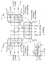
- This disclosure describes a boundary scan system where memories, i.e. flip flops or latches, used in data scan cells are also used functionally, but memories used in control scan cells are dedicated for test and not used functionally.
- the control scan cells can be scanned while the circuit is in functional mode, since their memories are dedicated.
- the data scan cells can only be scanned after the circuit transitions into test mode, since their memories are shared.
- This boundary scan system advantageously provides; (1) lower test circuitry overhead since the data scan cells use shared memories, (2) safe entry into test mode since the control scan cells can be scanned during functional mode to pre-load safe control conditions, and (3) avoidance of floating (i.e. 3-state) busses that can cause high current situations.
- the scan cell of Figure 2 can be accessed and pre-loaded with test data while the cell is in functional mode.
- the data scan cell associated with the D31 output of slave 1 104 is labeled to indicate the FDI 212, TDI 216, FDO 214, and TDO 218 signal connections of the Figure 2 scan cell.
- data is transferred from one of the slaves to the master via the 32-bit data bus (D0-31).
- the scan cells are transparent, allowing functional control and data signals to pass freely through the cells.
- the master enables slave 1 to transfer data by the ENA1 control signal, which is output from the master to slave 1.
- the master enables slave 2 to transfer data by the ENA2 control signal, which is output from the master to slave 2. While only two slave circuits are shown, any number could be similarly connected to and operated by the master. Since all the scan cells of the scan paths 108-112 are dedicated for test, they can be scanned from TDI to TDO without disturbing the functional mode of the Figure 1 circuit.
- the initial test pattern establishes both a data test pattern in the data scan cells (D) and a control test pattern in the control scan cells (C).
- D data test pattern
- C control test pattern
- the circuits can safely transition from a functioning mode to a test mode without concern over bus contention between the slave circuit's data busses.
- the ENA1 122 and ENA2 124 control scan cells (C) can be pre-loaded with control data to insure that only one of the slave's D0-31 data busses is enabled to drive the wired bus connection 126.
- Maintaining output drive on one of the slave data busses upon entry into test mode prevents the wired data bus 126 from entering into a floating (i.e. 3-state) condition. Preventing bus 126 from floating is desirable since a floating input to input buffers 128 of master 102 could cause a high current condition.
- a data scan cell (D) exists on each of the 32-bit data signal paths of each circuit 102-106
- a control scan cell (C) exists on each of the ENA1 and ENA2 control paths of each circuit 102-106.
- the 3-state control outputs 118-120 of the ENA1 and ENA2 control scan cells 122-124 do not ripple during the capture and shift part of the control input sequence. This is accomplished by having the data in M2_of Figure 2 be output, via MX2, during the capture and shift operation. Only during the update part of the control input sequence are the outputs 118-120 of the control scan cells 122-124 allowed to change state by new data being loaded into M2. Similarly, the outputs from the data scan cells (D) do not ripple during capture and shift operations, but rather change state only during the update part of the control input sequence.
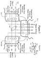
- Figure 3 illustrates a prior art example of a shared boundary scan path existing around a master 302 and slave circuits 304-306.
- the scan paths 308-312 around each circuit are connected together serially and to a test data input (TDI), which supplies test data to the scan paths, and a test data output (TDO), which retrieves data from the scan paths.
- TTI test data input
- TDO test data output
- the scan paths of Figure 3 are designed using shared scan cells (indicated by dashed circles), i.e. the scan cell memory is shared for both test and functional purposes.
- the shared scan cells of Figure 3 and subsequent Figures are shown positioned outside the boundary scan paths 308-312, whereas the dedicated scan cells of Figure 1 were shown positioned inside the boundary scan paths 108-112. Again, for simplification, only a portion of each circuits boundary scan path is shown.
- Figure 4 illustrates an example of a conventional shared scan cell consisting of a multiplexer (MX) 402 and a memory (M) 404.
- control inputs 406 form a path between FDI 408 and the data input of M 404 via MX 402, to allow functional data to be clocked from FDI to FDO 410.
- the control inputs 406 cause FDI data to be clocked into M via MX during a capture operation, and cause test data to be clocked from TDI 412 to TDO 414 during a shift operation. Since M 404 is used functionally, it cannot be accessed and pre-loaded with test data as can the scan cell of Figure 2.
- data is transferred from one of the slaves to the master via the 32-bit data bus (D0-31).
- the master enables data transfer from slave 1 or slave 2 via the ENA1 and ENA2 control signals, respectively. Since the scan cells of the scan paths are shared and used functionally, they cannot be scanned from TDI to TDO without disturbing the functional mode of the circuits. Not being able to scan data into the scan paths during functional mode prevents pre-loading an initial test pattern into the scan paths. By not being able to pre-load an initial test pattern into the scan paths, the slave circuits are put at risk of not safely transitioning into the test mode from the functional mode.
- the scan path of Figure 3 can be accessed to shift in test data.
- the outputs 318-320 of the control scan cells 322-324 ripple as data shifts through the cells.
- This output ripple from the control scan cells can cause the D0-31 output buffers of the slaves to be enabled and disabled during the shift operation.
- This control output ripple causes the output buffers of slaves 1 and 2 to be simultaneously enabled, again creating bus contention between the slaves.
- This voltage contention situation does not occur in the boundary scan path of Figure 1 since M 206 maintains a safe control output, via MX 208, during shift operations.
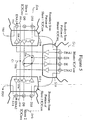
- Figure 5 shows one prior art technique for preventing the above mentioned two voltage contention situations. The technique is based on providing additional circuitry and control inputs to enable or disable the slave's output buffers during test mode entry and again during each test mode shift operation.
- a signal gating circuit 528 is inserted into signal path 518 of slave 504 and a signal gating circuit 530 is inserted into signal path 520 of slave 506.
- a control signal C1 532 is added as an input to circuits 528 and 530.
- C1 is in a first state, the ENA1 and ENA2 outputs from scan cells 522 and 524 are allowed to pass through circuits 528 and 530 to enable or disable the output buffers of slaves 504 and 506.
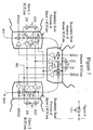
- Control for the multiplexers to select either the pathl's or path 2's between TDI and TDO come from a SEL signal which is connected to the select input of each multiplexer 636-640.
- the SEL signal 634 may come from an IEEE 1149.1 instruction register on the IC, another register or circuit on the IC, or from an input pin on the IC.
- the SEL signal may come from an IEEE 1149.1 instruction register on each of the ICs, another register or circuit on each of the ICs, or from an input pin on each of the ICs.
- the SEL signal will not be bussed to the same wire 634 as shown in Figure 6, but rather individual SEL signal wires will exist between the IEEE 1149.1 instruction register, or another register or circuit, and multiplexers 636-64 on each of the individual ICs.
- data is transferred from one of the slaves to the master via the 32-bit data bus (D0-31).
- the master enables data transfer from slave 1 or slave 2 via the ENA1 and ENA2 control signals, respectively. Since the data scan cells of the scan paths are shared and used functionally, they cannot be scanned from TDI to TDO without disturbing the functional mode of the circuits. However, since the control scan cells of the scan paths are not shared, they can be scanned from TDI to TDO without disturbing the functional mode of the circuit. By scanning the control scan cells by themselves, via path 1, it is possible to pre-load, while the master and slave circuits are functioning, a control test pattern into the control scan cells.
- This control test pattern can be advantageously used to establish the test mode state of the slave data busses to insure that no contention between the data busses occurs upon switching from functional mode to test mode.
- a control test pattern may be scanned into the control scan cells via path 1 to, upon entry into test mode, enable slave 1's data bus and disable slave 2's data bus or to disable slave 1's data bus and enable slave 2's data bus. So, by designing the control scan cells as dedicated scan cells, and by selectively grouping only the control scan cells onto pathl between TDI and TDO, it is possible to pre-load a control test pattern to safely transition into test mode without slave bus contention and without disabling both slave buses.
- the outputs of the data scan cells do ripple during shift operation since they use the scan cell design of Figure 4. However, this data ripple does not harm the circuit or cause bus contention since only one slave is enabled at a time to output data onto bus 626. While only two slave circuits 604 and 606, each with an associated boundary scan portions 608 and 612, were shown in Figure 6, any number of slave circuits and associated boundary scan portions could be similarly connected to the master circuit 602 and associated boundary scan portion 610.
- Figure 7 illustrates the boundary scan system of Figure 6 modified to include additional memories 702-712 in the path 1's.
- the wire runs between the scan inputs and outputs of the control scan cells in path 1 may become long when bypassing a large number of shared data scan cells. If the wiring becomes to long the setup and hold times of the control scan cells may be violated, resulting in shift operation failures through path 1.
- one or more resynchronization memories 702-712 may be located in path 1 between the scan outputs and scan inputs of the control scan cells.
- the resynchronization memories typically D flip flops as shown in Figure 8, would be located in scan path 1 such that the control data shifted through path 1 passes through a shorter length of wiring between the control scan cells and resynchronization memories, thus managing the setup and hold timing for reliably shifting data through path 1.
- the bit length of path 1 will grow by the number of resynchronization memories.
- each test pattern shifted into path 1 will need to be augmented to include appropriately positioned resynchronization data bits during shift operations.
- the resynchronization memories 702-712 are not necessary when shift operations occur through path 2, since the shared data scan cells are not being bypassed.
- scan path 2 does not include the resynchronization memories, and the test patterns shifted into scan path 2 advantageously do not need to be augmented to include the aforementioned resynchronization data bits.
- Figure 9 illustrates a boundary scan system consisting of master circuit 902 and slave circuits 904 and 906.
- Boundary scan portion 908 of slave 904 is similar to boundary scan portion 608 of Figure 6 with the exception that it includes an additional input (IN) to slave circuit 904 and an associated dedicated data scan cell 922.
- boundary scan portion 912 of slave 906 is similar to boundary scan portion 612 of Figure 6 with the exception that it includes an additional output (OUT) from slave circuit 906 and an associated dedicated data scan cell 924.
- Figure 9 is included to indicate that dedicated data scan cells 922 and 924 (i.e. a scan cell similar to that of Figure 2) can be included in both path 1 and path 2 shift operations.
- data can be shifted through the control scan cells (C) and the 922 and 924 data scan cells (D) of Figure 9 during functional mode.
- data can be shifted through all the scan cells of Figure 9, both shared and dedicated, during test mode.
- FIG. 6 and 9 and their accompanying descriptions have also described a process for safely transitioning circuits and their associated boundary scans paths from their functional mode to test mode.
- the process can be summarized as: (1) configuring the boundary scan path system to contain only dedicated scan cells between TDI and TDO, (2) performing a shift operation to load data into the dedicated scan cells, (3) entering the boundary scan test mode, (4) configuring the boundary scan path system to contain all scan cells, both shared and dedicated, between TDI and TDO, and (5) performing a shift operation to load data into all the scan cells.
Landscapes
- Engineering & Computer Science (AREA)
- General Engineering & Computer Science (AREA)
- Physics & Mathematics (AREA)
- General Physics & Mathematics (AREA)
- Tests Of Electronic Circuits (AREA)
- Test And Diagnosis Of Digital Computers (AREA)
- Semiconductor Integrated Circuits (AREA)
Abstract
Description
Claims (6)
- An integrated circuit comprising;a test data input terminal and a test data output terminal;a boundary scan path including one or more groups of serially connected dedicated boundary scan cells and one or more groups of serially connected shared boundary scan cells, said boundary scan path having an input and an output;a first connection formed between said test data input terminal and said boundary scan path input, and;a second connection formed between said test data output terminal and said boundary scan path output.
- The integrated circuit of Claim 1 further comprising;
a multiplexer circuitry associated with said boundary scan path for selectively bypassing said one or more shared boundary scan cell groups such that only the one or more dedicated boundary scan cell groups exist between said input and output. - The integrated circuit of Claim 1 or Claim 2 further comprising;
at least one resynchronization memory located in the serial path between at least two of said dedicated boundary scan cell groups. - A process of entering into a boundary scan test mode comprising the steps of;performing a first serial communication to load data into only a subset of the scan cells within the boundary scan path,entering the boundary scan test mode, and;performing a second serial communication to load data into all the scan cells within the boundary scan path.
- An integrated circuit comprising;
a boundary scan path having at least one resynchronization memory located in the serial path between two boundary scan cells. - An integrated circuit as claimed in any preceding claim and wherein said scan path or a portion thereof is realized as part of or interfaced with an embedded core.
Applications Claiming Priority (2)
| Application Number | Priority Date | Filing Date | Title |
|---|---|---|---|
| US17518800P | 2000-01-10 | 2000-01-10 | |
| US175188P | 2000-01-10 |
Publications (3)
| Publication Number | Publication Date |
|---|---|
| EP1130409A2 true EP1130409A2 (en) | 2001-09-05 |
| EP1130409A3 EP1130409A3 (en) | 2003-10-15 |
| EP1130409B1 EP1130409B1 (en) | 2005-11-09 |
Family
ID=22639305
Family Applications (1)
| Application Number | Title | Priority Date | Filing Date |
|---|---|---|---|
| EP20010200044 Expired - Lifetime EP1130409B1 (en) | 2000-01-10 | 2001-01-09 | Boundary scan path method and system |
Country Status (3)
| Country | Link |
|---|---|
| EP (1) | EP1130409B1 (en) |
| JP (1) | JP2001249168A (en) |
| DE (1) | DE60114681T2 (en) |
Cited By (1)
| Publication number | Priority date | Publication date | Assignee | Title |
|---|---|---|---|---|
| CN112462245A (en) * | 2019-09-09 | 2021-03-09 | 英业达科技有限公司 | Method and device for generating boundary scanning interconnection line |
Family Cites Families (2)
| Publication number | Priority date | Publication date | Assignee | Title |
|---|---|---|---|---|
| US5715254A (en) * | 1994-11-21 | 1998-02-03 | Texas Instruments Incorporated | Very low overhead shared resource boundary scan design |
| US5862152A (en) * | 1995-11-13 | 1999-01-19 | Motorola, Inc. | Hierarchically managed boundary-scan testable module and method |
-
2001
- 2001-01-09 DE DE2001614681 patent/DE60114681T2/en not_active Expired - Lifetime
- 2001-01-09 EP EP20010200044 patent/EP1130409B1/en not_active Expired - Lifetime
- 2001-01-10 JP JP2001002712A patent/JP2001249168A/en not_active Abandoned
Cited By (2)
| Publication number | Priority date | Publication date | Assignee | Title |
|---|---|---|---|---|
| CN112462245A (en) * | 2019-09-09 | 2021-03-09 | 英业达科技有限公司 | Method and device for generating boundary scanning interconnection line |
| CN112462245B (en) * | 2019-09-09 | 2022-08-19 | 英业达科技有限公司 | Method and device for generating boundary scanning interconnection line |
Also Published As
| Publication number | Publication date |
|---|---|
| EP1130409B1 (en) | 2005-11-09 |
| DE60114681D1 (en) | 2005-12-15 |
| DE60114681T2 (en) | 2006-07-20 |
| EP1130409A3 (en) | 2003-10-15 |
| JP2001249168A (en) | 2001-09-14 |
Similar Documents
| Publication | Publication Date | Title |
|---|---|---|
| US8667350B2 (en) | Multiplexers selectively coupling data scan cells in scan paths | |
| US10712387B2 (en) | First, second test domains and test mode select control circuitry | |
| US9121904B2 (en) | Tap linking module test access port controller with enable input | |
| US7694199B2 (en) | Three boundary scan cell switches controlling input to output buffer | |
| US7659741B2 (en) | Parallel scan distributors and collectors and process of testing integrated circuits | |
| US6728915B2 (en) | IC with shared scan cells selectively connected in scan path | |
| US7870449B2 (en) | IC testing methods and apparatus | |
| US8046649B2 (en) | Scan circuits formed peripheral of core circuits with control leads | |
| KR100469875B1 (en) | Real time data observation method and apparatus | |
| EP1130409B1 (en) | Boundary scan path method and system | |
| KR910007412B1 (en) | Integrated circuit of megacele method with a test ability |
Legal Events
| Date | Code | Title | Description |
|---|---|---|---|
| PUAI | Public reference made under article 153(3) epc to a published international application that has entered the european phase |
Free format text: ORIGINAL CODE: 0009012 |
|
| AK | Designated contracting states |
Kind code of ref document: A2 Designated state(s): AT BE CH CY DE DK ES FI FR GB GR IE IT LI LU MC NL PT SE TR |
|
| AX | Request for extension of the european patent |
Free format text: AL;LT;LV;MK;RO;SI |
|
| PUAL | Search report despatched |
Free format text: ORIGINAL CODE: 0009013 |
|
| AK | Designated contracting states |
Kind code of ref document: A3 Designated state(s): AT BE CH CY DE DK ES FI FR GB GR IE IT LI LU MC NL PT SE TR |
|
| AX | Request for extension of the european patent |
Extension state: AL LT LV MK RO SI |
|
| 17P | Request for examination filed |
Effective date: 20040415 |
|
| AKX | Designation fees paid |
Designated state(s): DE FR GB |
|
| 17Q | First examination report despatched |
Effective date: 20040601 |
|
| GRAP | Despatch of communication of intention to grant a patent |
Free format text: ORIGINAL CODE: EPIDOSNIGR1 |
|
| GRAS | Grant fee paid |
Free format text: ORIGINAL CODE: EPIDOSNIGR3 |
|
| GRAA | (expected) grant |
Free format text: ORIGINAL CODE: 0009210 |
|
| AK | Designated contracting states |
Kind code of ref document: B1 Designated state(s): DE FR GB |
|
| RAP1 | Party data changed (applicant data changed or rights of an application transferred) |
Owner name: TEXAS INSTRUMENTS INC. |
|
| REG | Reference to a national code |
Ref country code: GB Ref legal event code: FG4D |
|
| REF | Corresponds to: |
Ref document number: 60114681 Country of ref document: DE Date of ref document: 20051215 Kind code of ref document: P |
|
| ET | Fr: translation filed | ||
| PLBE | No opposition filed within time limit |
Free format text: ORIGINAL CODE: 0009261 |
|
| STAA | Information on the status of an ep patent application or granted ep patent |
Free format text: STATUS: NO OPPOSITION FILED WITHIN TIME LIMIT |
|
| 26N | No opposition filed |
Effective date: 20060810 |
|
| REG | Reference to a national code |
Ref country code: FR Ref legal event code: PLFP Year of fee payment: 16 |
|
| PGFP | Annual fee paid to national office [announced via postgrant information from national office to epo] |
Ref country code: GB Payment date: 20151230 Year of fee payment: 16 |
|
| PGFP | Annual fee paid to national office [announced via postgrant information from national office to epo] |
Ref country code: DE Payment date: 20160127 Year of fee payment: 16 |
|
| PGFP | Annual fee paid to national office [announced via postgrant information from national office to epo] |
Ref country code: FR Payment date: 20151230 Year of fee payment: 16 |
|
| REG | Reference to a national code |
Ref country code: DE Ref legal event code: R119 Ref document number: 60114681 Country of ref document: DE |
|
| GBPC | Gb: european patent ceased through non-payment of renewal fee |
Effective date: 20170109 |
|
| REG | Reference to a national code |
Ref country code: FR Ref legal event code: ST Effective date: 20170929 |
|
| PG25 | Lapsed in a contracting state [announced via postgrant information from national office to epo] |
Ref country code: FR Free format text: LAPSE BECAUSE OF NON-PAYMENT OF DUE FEES Effective date: 20170131 |
|
| PG25 | Lapsed in a contracting state [announced via postgrant information from national office to epo] |
Ref country code: GB Free format text: LAPSE BECAUSE OF NON-PAYMENT OF DUE FEES Effective date: 20170109 Ref country code: DE Free format text: LAPSE BECAUSE OF NON-PAYMENT OF DUE FEES Effective date: 20170801 |