Technical Field
The present invention relates to a mirror polishing
process for a semiconductor wafer (hereinafter, may be
simply referred to wafer), especially to a polishing pad
and polishing method used in a finish polishing as a
final step of polishing process for a semiconductor
wafer.
Background Art
Recently, with an ultra-miniaturization and higher
integration of semiconductor devices, it is desired that
a surface of a semiconductor wafer consisting of silicon
or the like is made flat with high precision.
Accordingly, a mirror polishing is performed as a
process means for answering the above-described desire.
By such a mirror polishing for a semiconductor wafer,
the wafer is processed to have a smooth and non-damage
mirror-polished surface.
As a conventional method for processing a
semiconductor wafer, there have been generally performed
a slicing step for slicing thin plates (wafers) from a
single crystal ingot, a chamfering step for preventing a
chipping in a peripheral portion of the wafer, a lapping
step or surface grinding step for reducing the
ununiformity of the thickness of a wafer, an etching
step for eliminating mechanical damages and contaminants,
a mirror-polishing step for mirror-surfacing a chamfered
portion and main surface of a wafer and the like
sequentially.
The mirror polishing for a silicon wafer is
performed by applying a constant load and relative speed
between the wafer and polishing pad while supplying a
polishing agent. For example, in the case where a
single-side polishing apparatus polishes a semiconductor
wafer, the polishing apparatus is mainly composed of a
turn table, wafer holder, and polishing agent supply
unit. The turn table, on which a polishing pad is
attached, is rotated at a predetermined rotation speed
via a rotary shaft. On the other hand, the structure of
the wafer holder is that it holds a wafer by means of
vacuum sucking, wax or the like, to face a polishing pad
attached on the turn table and presses the wafer against
the polishing pad with a predetermined load while
rotated via a rotating shaft. The polishing agent
supply unit supplies a polishing agent, which is made by
dispersing a calcined silica, colloidal silica or the
like in a alkaline solution, onto the polishing pad at a
predetermined flow rate, and during polishing, the wafer
is mirror-polished by supplying the polishing agent
between the wafer and the polishing pad.
As to mirror-polishing process, in addition to the
above-described single-side polishing apparatus, a
double-side polishing apparatus has also been employed,
which can make both sides of a wafer simultaneously like
a lapping process to be mirror-surface.
Further, as to wafer holding type, in addition to
the above-described types by means of vacuum sucking and
a wax type which holds a wafer with adhesive such as wax,
a wax free (waxless mount) type which holds a wafer with
a backing pad and template has been also employed. As
to the number of wafers to be processed, a so-called
batch processing type, which polishes multiple wafers
simultaneously, or a single wafer processing type, which
polishes wafers one by one, has been employed. As
described above, several processes and types for the
mirror polishing have been suggested from several
viewpoints.
Although any process or type as described above has
been employed, the mirror-polishing process is generally
performed under two or more steps. In a rough polishing
of the early step, called a first polishing, the
polishing is performed with a hard polishing pad at a
comparatively fast polishing rate so as to reduce the
ununiformity of the thickness of the wafer after
polishing.
However, in the polishing of the early step, there
are likely to remain the ununiformity of surface
roughness, a cloudiness so-called haze, for example, and
polishing damage, which becomes an issue on the
subsequent device fabrication process, on the wafer.
Accordingly, in general, a finish polishing process is
finally performed so that the ununiformity of surface
roughness which remains on the wafer surface is
eliminated to complete it as an entire mirror-polished
wafer.
In the early step of the polishing, that is, a
first polishing etc., a polishing pad which comprises a
foamed urethane sheet, or a polishing pad (velour type)
formed by impregnating urethane resin into a nonwoven
fabric such as polyester in order to harden it, is
generally used. Further, in a final finish polishing, a
suede-type polishing pad is used. This is as a sort of
artificial leather for industrial materials, and the
polishing pad, which comprises a base layer consisting
of a nonwoven fabric formed of a synthetic resin,
special synthetic rubber or the like, and a surface
layer consisting of a resin with high wear resistance
such as polyurethane and having minute pores formed
therein, is used. The back surface of the base layer is
bonded to a turn table with an adhesive double coated
tape or the like as a bond layer.
Incidentally, with a recent increase in the degree
of integration of semiconductor devices, the requirement
for the surface characteristic of wafers after mirror-polishing
process has became strict. For example, in
addition to the above-mentioned flatness of the wafer,
it has been required that even minute defects and
scratches on the wafer surface should not exist.
When the mirror-polishing process is performed,
minute damages or scratches may be generated on the
wafer surface, especially, in the early polishing step
such as a first polishing process, such polishing
damages or scratches are likely to be generated by using
a hard polishing pad or polishing agent having high
polishing performance. However, in the subsequent
finish polishing, the wafer is polished on the condition
to eliminate damages, scratches or the like, which
remain even after the first polishing as described above.
After the finish polishing, if there exist still
scratches or the like on the wafer surface, they are
detected by a common visual inspection under collimated
light, and the detected wafer is rejected as a defective
product. However, it is difficult to detect polishing
damages by the visual inspection under collimated light.
Therefore, after the finish polishing, even if such
damages exist on the wafer, they can not be detected on
the wafer surface, and thus the wafer has been regarded
as a non-defective product.
Further, even in a device fabrication stage, such a
wafer condition, that is, minute damage which exists
after finish polishing and can not be detected by a
visual inspection, has been disregarded as having no
harmful effects especially for quality (device
characteristic).
However, with a recent additional increase in the
degree of minuteness of devices, it has been suggested
that these damages may cause the problems in the device
fabrication process. In short, it has been observed
lowering yield and generating defects of unknown origin.
On the other hand, an evaluation technique for
wafer surface conditions has been improved, and as the
result, the polishing damages which could not be
detected in the past can be detected at present.
According to this evaluation method, it is found that
when the polishing is performed with a polishing pad for
a finish polishing, which has been used conventionally,
there are some cases where polishing damages generate on
the wafer surface. Judging from this, it is suggested
that these polishing damages may affect a device yield
for any reason. Its detailed action has not been
revealed, but it has been revealed that a minute damage
generated in a finish polishing process turns into some
defect nucleus, and it has a potential for causing a
failure of a semiconductor device.
The following results can also be obtained that the
polishing damages which remain on a wafer after a finish
polishing can not be reduced, even if polishing time or
the like is increased, and if anything, the finish
polishing time is longer, the generation of damages are
rather increased. Therefore, it was found that not so
much the polishing damages generated in the first
polishing process remain without being eliminated due to
insufficient polishing as new polishing damages generate
in the finish polishing process.
As described above, the polishing damages generated
in the finish polishing process to complete a high
quality wafer, which is suitable for a recent high-integrated
semiconductor device, are a particular
problem.
Disclosure of the Invention
The present invention has been accomplished in view
of the above-mentioned problems, and an object of the
present invention is to provide a polishing pad and
polishing method to obtain a mirror-polished wafer
without generating polishing damages in a mirror-polishing
process of a semiconductor wafer, especially
in a finish polishing.
In order to achieve the above object, the present
invention specifies the content of zinc compounds
included in a polishing pad so as not to generate
polishing damages in a mirror-polishing process. Zinc
weight relative to the weight of a polishing pad, used
in the present invention, means weight of zinc which
constitutes zinc compounds included in the polishing
pad/weight of the polishing pad, as long as it has no
particular notice.
The present invention provides a polishing pad used
for mirror-polishing a semiconductor wafer, wherein a
content of zinc compounds included in the polishing pad
is 200ppm or less at the ratio of zinc weight relative
to the weight of the polishing pad.
As described above, if the polishing pad, in which
the content of zinc compounds included is 200ppm or less
at the ratio of zinc weight relative to the weight of
the polishing pad, is used in a mirror-polishing, the
polishing damages generated in the mirror-polishing can
be suppressed, and accordingly the wafer having almost
no problem in the subsequent device fabrication process
can be manufactured.
Also, the present invention provides a polishing
pad used for mirror-polishing a semiconductor wafer in a
finish polishing process, wherein a content of zinc
compounds included in the polishing pad is 100ppm or
less at the ratio of zinc weight relative to the weight
of the polishing pad.
As described above, if the polishing pad, in which
the content of zinc compounds included is defined to a
less extent as 100ppm or less at the ratio of zinc
weight relative to the weight of the polishing pad, is
used to eliminate cloudiness and polishing damages in
the finish polishing, the polishing damages generated in
the finish polishing are further suppressed and
accordingly the wafer having almost no problem in the
subsequent device fabrication process can be
manufactured.
Further, the present invention provides a polishing
pad used for mirror-polishing a semiconductor wafer in a
finish polishing process, wherein the polishing pad does
not include zinc compounds.
As to the polishing pad used for the finish
polishing, it is preferable that the polishing pad
includes zinc compounds as little as possible, and
therefore, use of the polishing pad including no zinc
compounds as described above can suppress the generation
of polishing damages.
Furthermore, it is preferable that the polishing
pad according to the present invention in which the
content of zinc compounds is controlled comprises a base
layer consisting of a nonwoven fabric and a porous
surface layer.
As described above, by using the polishing pad
which comprises a base layer consisting of a nonwoven
fabric and a porous surface layer, in the case of a
polishing, the polishing can be preferably performed
without causing the polishing damages on a wafer surface
due to zinc compounds in the polishing pad.
In this case, the polishing pad is more preferred
such that the content of zinc compounds included in the
surface layer is 100ppm or less at the ratio of zinc
weight relative to the weight of the surface layer.
As described above, it is preferable that the
polishing pad includes zinc compounds as little as
possible. However, zinc compounds which actually cause
polishing damages are included in the portion where the
polishing pad is in contact with a wafer, that is, zinc
compounds included in the surface layer of the polishing
pad cause polishing damages. Therefore, it is important
that zinc compounds included in the surface layer of the
polishing pad should be less.
As described above, by using the polishing pad in
which the content of zinc compounds included in the
surface layer of the polishing pad is 100ppm or less at
the ratio of zinc weight relative to the weight of the
surface layer, zinc compounds which exist in the contact
portion with a wafer can be certainly reduced, and in
the case of polishing, the polishing can be performed
more preferably without causing the polishing damages on
a wafer surface.
As to the content of zinc compounds in the base
layer, it is not limited in particular as long as the
content of zinc compounds included in the surface layer
is 100ppm or less at the ratio of zinc weight relative
to the weight of the surface layer. However, it is
preferable that the content of zinc compounds in the
base layer as well as in the surface layer is as little
as possible. By the way, it is preferable in particular
that the surface layer does not include zinc.
Further, it is preferable in particular that the
surface layer is formed of foamed polyurethane. A
conventional polishing pad including urethane resin
suffers from a problem that it is likely to include zinc
compounds in particular. On the contrary, as described
above, by using the polishing pad which has a surface
layer formed of polyurethane and is controlled in terms
of the content of zinc compounds in the entire polishing
pad or the surface layer of the polishing pad, the wafer
having very little damages can be manufactured. Also,
since the surface layer is formed of foamed polyurethane,
the mirror polishing of high surface precision and the
finish polishing of high surface precision, such as
removal of cloudiness, can be preferably performed.
Furthermore, the present invention provides a
method for polishing a semiconductor wafer using the
aforementioned polishing pad. If the polishing pad
specified in terms of the content of zinc compounds as
aforementioned is applied to the mirror polishing of a
semiconductor wafer, especially to the finish polishing,
the semiconductor wafer which has almost no damages and
which is suitable for fabricating a high-integrated
semiconductor device can be manufactured.
Additionally, the present invention provides a
polishing method for a semiconductor wafer, wherein a
finish-polishing in a mirror-polishing of the
semiconductor wafer is performed on the condition that
the concentration of zinc compounds in the position
where the semiconductor wafer is in contact with the
polishing pad is 200ppm or less.
As aforementioned, the mirror polishing of a
semiconductor wafer is generally performed stepwise so
that a finish polishing is performed after a rough
polishing such as a first polishing. However, if zinc
compounds are included in the finish polishing, in what
way, for example, from a polishing agent, damages are
obliged to generate. That is, the problem lies in the
fact that zinc compounds exist between a polishing pad
and wafer. Therefore, as described above, if a finish-polishing
is performed on the condition that the
concentration of zinc compounds in the position where a
semiconductor wafer is in contact with the polishing pad
is 200ppm or less, the semiconductor wafer suitable for
fabricating high integrated semiconductor devices can be
produced without the generation of polishing damages.
That is, the content of zinc compounds present in
the polishing agent or polishing pad is reduced to the
utmost, in fact, the less content of zinc compounds is
more preferable. Specifically, when the concentration
of zinc compounds in the position where a semiconductor
wafer is in contact with the polishing pad is 200ppm or
less, the polishing damages, which may cause the
generation of defects or low yield in the subsequent
device fabrication step, can be suppressed.
It is clear from the above explanation that the
content of zinc compounds in the polishing pad or the
concentration of zinc compounds in the portion where the
polishing pad is in contact with a wafer during the
polishing is controlled at a certain amount or less, so
that a high quality wafer having very few polishing
damages can be manufactured.
Further, thus manufactured wafer having very few
polishing damages can be applied to fabrication of
recent high-integrated devices. By using this wafer,
the generation of defects and low yield in the
subsequent device fabrication step can be improved.
Furthermore, by reducing the content of zinc
compounds, a processing time of a polishing pad in
start-up can be reduced, and as the result, operating
efficiency can be increased.
Brief Description of the Drawings
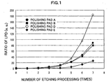
FIG. 1 is a graph representing the relation between
the number of etching and ratio of LPD in terms of each
polishing pad used in the examples and comparative
example.
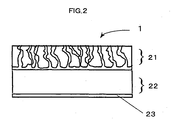
FIG. 2 is a schematic cross sectional view showing
one example of a polishing pad used in a finish
polishing.
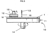
FIG. 3 is a schematic view showing a structure of
polishing portion of a single-side polishing apparatus
for mirror-polishing a surface of a semiconductor wafer.
Best Mode for Carrying out the Invention
An embodiment of the present invention will now be
described; however, the present invention is not limited
thereto.
The present inventors found that minute polishing
damages were generated by using a conventional finish
polishing pad in a mirror-polishing process of a
semiconductor wafer, examined the polishing damages
generated in the polishing process, and found that some
contaminants were included in the polishing pad. These
contaminants, were identified by Energy Dispersive X-ray
Spectroscopy (abbreviated name, EDX), as the result,
zinc (Zn) and oxygen (O) were detected, and it was found
that these contaminants were zinc compounds. Further,
it was revealed that a wafer polished by a polishing pad
having more zinc compounds was likely to generate more
surface defects than a wafer polished by a polishing pad
having less zinc compounds.
Consequently, the inventors investigated the
inclusion of zinc compounds, and found that zinc
compounds were added to a polishing pad for controlling
its characteristic in manufacturing thereof. For
example, zinc compounds are added to a polishing pad for
increasing hardness of a nonwoven fabric constituting
the polishing pad. Additionally, zinc compounds were
added to a polishing pad formed of urethane resin as a
stabilizer against light in a manufacturing step of
urethane resin, and it was found that not a little zinc
compound were included into the polishing pad
manufactured based on the above urethane resin.
Conventional polishing pads investigated this time
included zinc compounds of several hundred ppm.
This zinc compound is mainly composed of zinc oxide
(ZnO), and its grain diameter is about 500nm to 1000nm.
It was revealed that if such zinc compounds are included
in a polishing pad, the generation of surface defects on
a wafer is accelerated when the wafer surface is
polished by using the polishing pad.
A zinc compound is generally a softer substance than
silicon, which is used as a raw material of a
semiconductor wafer. That is, indicating by Mohs
hardness, the hardness of silicon (Si) as a polished
material is 7, silica (SiO2) of a polishing agent is 7,
and zinc compound (ZnO) is 4. Therefore, as to hardness,
since silicon is harder than zinc compound, it seemed
difficult to generate scratches due to the zinc compound,
so that it has not been studied the influence of zinc
compound in the polishing.
However, the present inventors devoted themselves
to investigation on the influence, and revealed for the
first time that although each wafer surface has no
visible scratches so far as the detection by a visual
inspection under collimated light or the like, each
wafer surface is differently damaged in accordance with
the difference of the content of zinc compounds in each
polishing pad.
Further, it is considered that this damage
functions as a defect nucleus in the subsequent step,
and leads to generation of defects which may lower
dielectric breakdown strength of oxide film or affect
yield.
Consequently, the present invention provides a
polishing pad for semiconductor wafer, wherein the
content of zinc compounds thereof is controlled.
First, with reference to the drawings, there will
be described one example of a mirror-polishing apparatus
to which a polishing pad for semiconductor wafer
according to the present invention can be applied.
FIG. 3 is a schematic view showing a structure of
polishing portion of a single-side polishing apparatus.
The single-side polishing apparatus as shown in FIG. 3
is constructed to polish a single side of a
semiconductor wafer, for example, and as shown in the
drawing, the polishing portion 10 of the polishing
apparatus generally comprises a turn table 11, wafer
holder 12 (sometimes called head), and polishing agent
supply unit 13. A polishing pad 1 is applied to the top
surface of the turn table 11, and the polishing pad 1
together with the turn table 11 is rotated by a rotary
shaft 14 at a predetermined rotating speed.
And, the wafer holder 12 holds a wafer W with vacuum
sucking, wax, or the like so that the wafer faces the
polishing pad on the turn table, and presses the wafer W
against the polishing pad 1 at a predetermined load in
parallel with the rotation of the rotating shaft 15.
The polishing agent supply unit 13 supplies a
polishing agent 16 onto the polishing pad 1 at a
predetermined flow rate, and the polishing agent 16 is
supplied between the wafer W and polishing pad 1, so
that the wafer W is polished smoothly.
Next, one example of a polishing pad used for mirror
polishing will now be described with reference to FIG. 2.
The polishing pad 1, which is used for mirror-polishing
the surface of a semiconductor wafer with
aforementioned single-side polishing apparatus, for
example, is a suede-type polishing pad for finish-polishing
comprising a base layer 22 formed of nonwoven
fabricand porous surface layer 21 (the surface layer 21
sometimes called a nap layer) formed on the base layer
22. This polishing pad is adhered to the turn table 11
as shown in FIG. 3 through a bond layer 23 such as
adhesive double coated tape. By the way, when the
polishing is performed, as aforementioned, the wafer W
held by the wafer holder 12 is polished by being pressed
onto the polishing pad 1 with a predetermined load while
the polishing agent 16 is supplied onto the polishing
pad 1 rotated at a predetermined rotation speed.
A polishing pad for semiconductor wafer according to
the present invention is characterized in that the
content of zinc compounds included in the polishing pad
is 200ppm or less at the ratio of zinc weight relative
to the weight of the polishing pad. Such a polishing
pad is used for mirror-polishing a semiconductor wafer,
so that polishing damages which may be generated in
mirror-polishing are suppressed, and therefore, the
wafer having almost no trouble for the subsequent device
fabrication step can be manufactured.
Besides, specifically, when mirror-polishing is
performed stepwise, that is, when a finish polishing is
performed after rough-polishing such as a first
polishing and second polishing, polishing damages can be
eliminated more certainly in the finish polishing by
using a polishing pad in which the content of zinc
compounds is 100ppm or less at the ratio of zinc weight
relative to the weight of the polishing pad, so that the
wafer having almost no problem in the subsequent device
fabrication step can be manufactured.
Further, it is preferable that the polishing pad
includes zinc compounds as little as possible, and if a
polishing pad having no zinc compounds is used for a
finish polishing, polishing damages due to zinc
compounds are not generated completely, and therefore,
the wafer can be suitable for high-integrated
semiconductor devices.
As to material and structure of the polishing pad,
any polishing pad used conventionally can be available,
however, considering elimination of cloudiness on the
wafer surface after polishing, it is preferable to use a
suede-type polishing pad comprising a base layer
consisting of nonwoven fabric and porous surface layer
as shown in FIG. 2. Such a polishing pad, which is
formed of the base layer and surface layer and is
controlled in terms of the content of zinc compounds, is
used for mirror-polishing of a semiconductor wafer,
specifically, finish polishing thereof, so that the
semiconductor wafer can be finished without cloudiness,
and besides without polishing damages which may become
defect nuclei. And thus obtained wafer can be
advantageously used in the subsequent device fabrication
process.
Furthermore, as described above, the content of zinc
compounds in the polishing pad comprising a base layer
consisting of nonwoven fabric and a porous surface layer
is preferably as little as possible in both the base
layer and surface layer, especially, rather preferably
as little as possible in the surface layer, and
specifically, the content of zinc compounds included in
the surface layer is 100ppm or less at the ratio of zinc
weight relative to the weight of the surface layer.
When a mirror polishing of a wafer is performed by
using the polishing pad according to the present
invention, only a surface layer of the polishing pad is
actually in contact with the wafer surface to polish it.
Therefore, the existence of polishing damages depends
largely on the content of zinc compounds in the portion
where the polishing pad is in contact with the wafer,
that is, in the surface layer. Therefore, for example,
even if the content of zinc compounds included in the
polishing pad is more than 100ppm at the ratio of zinc
weight relative to the weight of the polishing pad, but
if the content of zinc compounds in the surface layer
thereof is 100ppm or less, the very excellent wafer
having no polishing damages can be completed. In this
case, it needs an attention so that zinc compounds
should not be transferred from the base layer to the
surface layer.
The material of the surface layer is not limited as
far as it has been conventionally used as a polishing
pad, but foamed polyurethane is preferred in particular.
For example, if a nonwoven fabric, which has been
conventionally employed, is used as the base layer, and
the surface layer consists of foamed polyurethane,
coupled with the limitation of the content of zinc
compounds included in the polishing pad or surface layer
thereof, a mirror polishing of a semiconductor wafer,
especially a finish polishing of a silicon wafer can be
preferably performed, and thereby the wafer can be
finished without polishing damages.
The polishing pad according to the present invention
is controlled in terms of the content of zinc compounds
included in the polishing pad as aforementioned, and if
such a polishing pad is used for mirror-polishing,
especially for finish-polishing, the wafer having no
polishing damages can be obtained. And, it is
considered that thus effect comes from keeping the
concentration of zinc compounds to a certain rate or
less in the portion where the polishing pad is in
contact with a wafer. Therefore, if a mirror polishing,
especially a finish polishing is performed on the
condition that the concentration of zinc compounds in
the portion where the polishing pad is in contact with
the wafer is suppressed to a certain rate or less, the
wafer having no polishing damages can be obtained.
In a common finish polishing process, it is very
rare case that zinc compounds come from outside.
Therefore, if only the content of zinc compounds in the
polishing pad is limited, the concentration of zinc
compounds in the portion where the polishing pad is in
contact with the wafer can be suppressed to a certain
rate or less, and the wafer can be preferably polished.
In this case also, it is preferable that the polishing
pad includes zinc compounds as little as possible, but
even if there is a factor from outside except the
polishing pad, if a finish polishing is performed on the
condition that the concentration of zinc compounds in
the portion where the polishing pad is in contact with a
semiconductor wafer is collectively 200ppm or less, the
same effect as described above, that is, the wafer
having no polishing damages can be obtained.
As described above, the polishing pad and polishing
method according to the present invention are applied to
a mirror polishing of a semiconductor wafer, especially
to a finish polishing, so that the wafer can be finished
without polishing damages. Further, when the resultant
wafer is used, the generation of failure in the
subsequent device fabrication step can be suppressed.
Furthermore, since the polishing pad according to
the present invention is hyhrophilic because of low
content of zinc compounds, working effeciency can also
be improved in the beginning step of using the polishing
pad. Generally, in the beginning step of using a
polishing pad for a finish polishing or the like, first,
a start-up process (sometimes called a dummy polishing)
is performed to make the surface layer of the polishing
pad familiar with polishing agent or water and makes
better contactability between the wafer and polishing
pad in polishing, and thereby accuracy of a mirror-surface
process is improved. However, the polishing pad
according to the present invention, as mentioned above,
is hyhrophilic, so that it is easy to become familiar
with water, and the start-up process time can be reduced.
Therefore, working efficiency, especially in the
beginning step of polishing pad, is improved, and the
whole polishing operation time is also reduced.
By the way, the polishing pad and polishing method
according to the present invention are applicable to
apparatuses or manners, not limited in particular, as
far as they are used for mirror-polishing a
semiconductor wafer. For example, besides a single-side
polishing method, double-side polishing method can also
be used. Further, the present invention is not
especially limited to any wafer holding method, and thus
any types of a vacuum sucking type, wax type or wax free
type can be adopted, and a batch type process, by which
multiple wafers are polished at once, or a single wafer
processing method, by which a wafer is polished one by
one, can be also applied. As described above,
apparatuses of various methods and types performed in
mirror polishing can be applied.
Further, the present invention is not also limited
in a semiconductor wafer to be polished in particular,
but specifically can be applied to a silicon single
crystal wafer preferably.
Incidentally, the present invention is adapted to a
common wafer process, that is, a finish polishing in a
multi-step polishing process, however, as examples
except such a finish polishing, the present invention
can also be applied to a polishing for a wafer processed
by PACE (Plasma Assisted Chemical Etching) technique
which is a thinning method different from grinding and
polishing and has been developed in recent years, or by
hydrogen ion delaminating method (sometimes called a
smart cut method) which has been suggested as a thin SOI
(Silicon On Insulator) film manufacturing technique.
Since the mirror surface condition of a wafer is
slightly degraded after hydrogen ion delamination or by
performing PACE process, a light polishing called touch
polishing whose stock removal is about tens of nm is
performed. It is preferable that polishing damages are
not existed also in such processes, and therefore the
polishing pad of the present invention can be applied
thereto.
Hereinafter, the present invention will now be
specifically described, giving examples and comparative
example; however, the present invention is not limited
thereto.
It becomes a problem that damages remain on a wafer
surface especially before device fabrication step, that
is, after a finish polishing so as to attain the final
quality of a wafer.
Accordingly, in the following examples and
comparative example, a silicon single crystal wafer
(diameter/150mm and thickness/625µm) after a first
polishing was used as an example to be polished, and the
influence of zinc compounds in the finish polishing was
determined.
A polishing pad, in which a base layer consists of
a nonwoven fabric having a thickness of about 1000µm
and formed by impregnating a polyester felt with
polyurethane, a polyurethane was coated (laminated) on
the base layer, a foam layer was grown in the
polyurethane, and a surface portion of the foam layer
was eliminated to form openings in the foam layer
thereby forming a nap layer having a thickness of about
450µm, was used.
Example 1 and Example 2
The content of zinc compounds in polishing pads
were adjusted (reduced) by changing an additive amount
of zinc compounds to the surface layer in manufacturing
the polishing pad. According to such a method, the
polishing pads in which the content of zinc compounds
included in a surface layer of the polishing pad was 40-100ppm
at the ratio of zinc weight relative to the
weight of the surface layer in the polishing pad were
obtained. In the present examples, two kinds of
polishing pads that one was 99ppm at the ratio of zinc
weight relative to the weight of the surface layer of
the polishing pad (polishing pad A; Example 1), and the
other was 78ppm (polishing pad B; Example 2) were used,
and the influence of zinc compounds in a finish
polishing was determined.
As to zinc weight relative to the weight of the
surface layer of the polishing pad, the surface layer of
the polishing pad was decomposed with a microwave (MW),
and the weight was determined by an atomic absorption.
Specifically, a foamed polyurethane in a surface
layer of the polishing pad was cut off (sampling) by
10mg with a ceramic cutter, the sample was dissolved by
using a MW decomposing apparatus (made by Perkin-Elmer
Corporation) with HNO3 of 6mL used as a resolvent
solution, and after that, the content of zinc (Zn) was
determined by an atomic absorption apparatus (made by
Perkih-Elmer Corporation, SIMAA 6000).
The lower limit of detection in the atomic
absorption apparatus itself was about 10ppb, the lower
limit of detection under this evaluation method as a
whole (the lower limit value of reliable values obtained
by repeated measurements, for example), which varied
with the quantity of sampling, or the quantity of
dilution in analysis, is about 10ppm. By the way, the
content of Zn determined here was expressed in a formula
[zinc weight constituting zinc compounds included in the
sampled surface layer of the polishing pad/weight of the
sampled surface layer of the polishing pad].
Hereinafter, this may be merely called zinc content in a
surface layer.
Further, zinc weight relative to total weight of a
polishing pad including a base layer was determined by
the same method as aforementioned except a measurement
example which was obtained by cutting out, not only a
foamed polyurethane of its surface layer, but a
polishing pad as a whole including its base layer with a
ceramic cutter. That is, after dissolving the sample by
a microwave, its solution was determined by an atomic
absorption.
The zinc content in the polishing pad measured by
this method was 255ppm in the polishing pad A and 195ppm
in the polishing pad B.
As for polishing condition, a single-side polishing
apparatus as shown in FIG. 3 was used, and polishing was
performed at a polishing load of 100g/cm2, head rotation
number of 80rpm, and turn table rotation number of 80rpm
while supplying a colloidal silica (particle diameter/
about 80nm, silica concentration/ 2.5 weight %, and pH/
10.5) used as a polishing agent at 150cc/min. The
polishing time was 10 minutes, and the stock removal was
about 0.1µm.
Defects (polishing damages) on a wafer surface were
evaluated after polishing the wafer. The evaluation of
defects on a wafer surface was performed by processing
it with an ammonia-type processing liquid, and then
observing the number of LPD (Light Point Defect). This
is the evaluation method by utilizing a phenomenon that
when there are defects such as polishing damages on a
wafer surface, if the processing is performed by using
an ammonia hydrogen peroxide-type processing liquid for
a certain period of time, and as the result, the number
of LPD is rapidly increased (extraordinarily increased).
If polishing damages are large, the number of LPD is
extraordinarily increased in the early step of a
processing time.
Specifically, the evaluation was performed by
etching a wafer surface for a certain period of time (20
minutes in the present example) with a processing liquid
composed of ammonia, hydrogen peroxide and water, and
then counting the number of LPD of 0,12µm or more
formed on the wafer surface by a particle counter LS6000
(made by Hitachi Electronics Engineering Co., Ltd.). By
repeating such an operation of counting LPDs after
etching process for a certain period of time, the
alteration of the number of LPD based on the processing
time (processing number of times) was evaluated. In
this case, the processing liquid was composed of ammonia
whose concentration was 0.3 weight %, hydrogen peroxide
whose concentration was 0.15 weight %, and a purified
water used as the rest.
The results of the evaluation was as follows.
In the polishing pad A (Example 1), the number of
LPD was 13.5 particles/cm2 when the processing time was
120 minutes (20-minutes processing was repeated 6 times),
and after that, the number of LPD was about 25.7
particles/cm2 when the processing time was 140 minutes.
In the polishing pad B (Example 2), the number of LPD
nearly equal to the polishing pad A was detected,
however, the increase of the LPD in the case of the
polishing pad B having less content of zinc compounds in
the wafer surface was smaller than that of the LDP in
the case. of the polishing pad A.
Comparative example
Next, a polishing was performed by using a
conventionally used polishing pad. The content of zinc
compounds in a surface layer of conventionally used
polishing pads is generally about 300-800ppm at the
ratio of zinc weight relative to the weight of the
surface layer of the polishing pad, or 1000ppm or more
in the case of a plenty one.
The content of zinc compounds in a surface layer of
these polishing pads is approximately consistent in each
kind of polishing pads or each of production batches,
but the contents have not been controlled.
Consequently, a finish polishing was performed on
the same condition as Example 1 by using a conventional
polishing pad (zinc content in a surface layer of the
polishing pad was 1008pm, and zinc content in the
polishing pad was 2500ppm; polishing pad D; Comparative
example).
In the polishing pad D (Comparative Example), the
number of LPD after polishing the wafer was already
increased up to 27.6 particles/cm2 when the processing
time was 120 minutes, and after that, the number of LPD
was increased up to 53.5 particles/cm2 when the
processing time was 140 minutes.
The relation between the number of etching and the
ratio of LPD in each polishing pad used in Examples 1
and 2 and Comparative Example is shown in FIG. 1.
In this graph, an abscissa axis indicates the
number of etching process performed by using an ammonia-type
processing liquid (substantially corresponding to
processing time), and an ordinate axis indicates the
ratio of LPD (substantially corresponding to the number
of LPD) on the basis of a case of the polishing pad B
(wherein the number of LPD after round of 7 times
processes is regarded as 80). Incidentally, FIG. 1 also
includes the results of Example 3 (polishing pad E)
described later.
It is clear from the graph that as compared a
Comparative example (polishing pad D) with Examples 1
and 2 (polishing pads A and B), the content of zinc
compounds in the surface layer affects the increase of
the number of LPD. Namely, in the case of using the
polishing pad D, it is observed that LPDs are increased
about twice as many as the case of using the polishing
pad A or B. It is clear that the difference of damages
existing in the wafer surface is due to the difference
of the content of zinc compounds included in the
polishing pad, especially in the surface layer of the
polishing pad.
Also, it is expected that there are also defects
induced by these damages. Actually, wafers polished by
the same type polishing pad as the polishing pad D of
Comparative example had the higher probability of the
generation of defects or decrease of yield in a device
fabrication step.
Example 3
Next, on the same condition as Example 1, a
polishing was performed by using a polishing pad having
no zinc compounds, specifically a polishing pad having
zinc compounds of the lower limit of detection (10ppm)
or less detected by the aforementioned Zn content
evaluation method.
As to the content of zinc compounds in the
polishing pad, the concentration of zinc in a raw
material of the polishing pad was determined in a
production step of polyurethane, and the polishing pad,
which was produced on the condition that the
concentration of zinc was controlled to be the lower
limit of detection, was used. Also, the addition of
zinc compounds or the like was not performed. Thus
produced polishing pad has no problem of its physical
characteristics (such as hardness).
Although there exists a question of measurement
accuracy, the content of zinc in the surface layer and
the content of zinc in the polishing pad were determined,
and accordingly the content of zinc in the surface layer
was about 1ppm, and the content of zinc in the polishing
pad was about 2.5ppm (polishing pad E, Example 3).
As to damages on the wafer surface after polishing
by using the polishing pad E on the same condition as
the aforementioned Examples 1 and 2, as shown in FIG. 1,
the number of LPD in the case of the polishing pad E was
much smaller than that of LPD in the case of the
polishing pad B, and it was about 30 percent of the
latter when the processing was repeated seven times.
That is, it is found that the increase of the number of
LPD was very little, and therefore the wafer having
little polishing damages was manufactured.
(Test)
Further, in a finish polishing step commonly
performed at present, only a polishing pad has zinc
compounds, and accordingly it has little possibility
that zinc compounds come from the outside factor such as
a polishing agent.
Therefore, if a control of polishing pads is
performed, it will be sufficient, however, for example,
the influence where zinc compounds would come from the
outside was determined. That is, a polishing was
performed with a polishing agent intentionally including
zinc oxides. Specifically, the polishing was performed
with the polishing agent including zinc oxides (particle
diameter was 500nm or more) of about 3mg in the
polishing agent of 1 liter.
As the result of this, the considerable number of
polishing damages was observed. That is, it is clear
that the amount of zinc compounds in the portion where a
wafer is in contact with zinc compounds during polishing
is important. Namely, polishing damages are also
generated on the condition that zinc compounds come from
anywhere except a polishing pad, therefore, it is
important that the concentration of zinc compounds in
the portion with which the wafer is in contact is
controlled. Conversely, if a polishing is performed by
controlling the concentration of zinc compounds in that
portion, polishing damages can be suppressed.
The present invention is not limited to the above-described
embodiments. For example, in the abovedescribed
embodiments, a single-side polishing apparatus
is mainly used, but a double-side polishing apparatus
can be also used. That is, the polishing pad and
polishing method according to the present invention can
be applied to all of apparatuses for polishing a wafer.
Further, as to types of polishing, the present invention
is not limited to a single wafer processing which
polishes wafers one by one, and thus can be applied to
all processing types including batch processing which
polishes a plurality of wafers simultaneously.