EP1129473B1 - Conductive isostructural compounds - Google Patents
Conductive isostructural compounds Download PDFInfo
- Publication number
- EP1129473B1 EP1129473B1 EP99968846A EP99968846A EP1129473B1 EP 1129473 B1 EP1129473 B1 EP 1129473B1 EP 99968846 A EP99968846 A EP 99968846A EP 99968846 A EP99968846 A EP 99968846A EP 1129473 B1 EP1129473 B1 EP 1129473B1
- Authority
- EP
- European Patent Office
- Prior art keywords
- compounds
- kpb
- isostructural
- thermoelectric
- present
- Prior art date
- Legal status (The legal status is an assumption and is not a legal conclusion. Google has not performed a legal analysis and makes no representation as to the accuracy of the status listed.)
- Expired - Lifetime
Links
Images




Classifications
-
- H—ELECTRICITY
- H10—SEMICONDUCTOR DEVICES; ELECTRIC SOLID-STATE DEVICES NOT OTHERWISE PROVIDED FOR
- H10N—ELECTRIC SOLID-STATE DEVICES NOT OTHERWISE PROVIDED FOR
- H10N10/00—Thermoelectric devices comprising a junction of dissimilar materials, i.e. devices exhibiting Seebeck or Peltier effects
- H10N10/80—Constructional details
- H10N10/85—Thermoelectric active materials
- H10N10/851—Thermoelectric active materials comprising inorganic compositions
- H10N10/853—Thermoelectric active materials comprising inorganic compositions comprising arsenic, antimony or bismuth
-
- C—CHEMISTRY; METALLURGY
- C04—CEMENTS; CONCRETE; ARTIFICIAL STONE; CERAMICS; REFRACTORIES
- C04B—LIME, MAGNESIA; SLAG; CEMENTS; COMPOSITIONS THEREOF, e.g. MORTARS, CONCRETE OR LIKE BUILDING MATERIALS; ARTIFICIAL STONE; CERAMICS; REFRACTORIES; TREATMENT OF NATURAL STONE
- C04B35/00—Shaped ceramic products characterised by their composition; Ceramics compositions; Processing powders of inorganic compounds preparatory to the manufacturing of ceramic products
- C04B35/515—Shaped ceramic products characterised by their composition; Ceramics compositions; Processing powders of inorganic compounds preparatory to the manufacturing of ceramic products based on non-oxide ceramics
- C04B35/547—Shaped ceramic products characterised by their composition; Ceramics compositions; Processing powders of inorganic compounds preparatory to the manufacturing of ceramic products based on non-oxide ceramics based on sulfides or selenides or tellurides
-
- C—CHEMISTRY; METALLURGY
- C30—CRYSTAL GROWTH
- C30B—SINGLE-CRYSTAL GROWTH; UNIDIRECTIONAL SOLIDIFICATION OF EUTECTIC MATERIAL OR UNIDIRECTIONAL DEMIXING OF EUTECTOID MATERIAL; REFINING BY ZONE-MELTING OF MATERIAL; PRODUCTION OF A HOMOGENEOUS POLYCRYSTALLINE MATERIAL WITH DEFINED STRUCTURE; SINGLE CRYSTALS OR HOMOGENEOUS POLYCRYSTALLINE MATERIAL WITH DEFINED STRUCTURE; AFTER-TREATMENT OF SINGLE CRYSTALS OR A HOMOGENEOUS POLYCRYSTALLINE MATERIAL WITH DEFINED STRUCTURE; APPARATUS THEREFOR
- C30B11/00—Single-crystal growth by normal freezing or freezing under temperature gradient, e.g. Bridgman-Stockbarger method
-
- C—CHEMISTRY; METALLURGY
- C30—CRYSTAL GROWTH
- C30B—SINGLE-CRYSTAL GROWTH; UNIDIRECTIONAL SOLIDIFICATION OF EUTECTIC MATERIAL OR UNIDIRECTIONAL DEMIXING OF EUTECTOID MATERIAL; REFINING BY ZONE-MELTING OF MATERIAL; PRODUCTION OF A HOMOGENEOUS POLYCRYSTALLINE MATERIAL WITH DEFINED STRUCTURE; SINGLE CRYSTALS OR HOMOGENEOUS POLYCRYSTALLINE MATERIAL WITH DEFINED STRUCTURE; AFTER-TREATMENT OF SINGLE CRYSTALS OR A HOMOGENEOUS POLYCRYSTALLINE MATERIAL WITH DEFINED STRUCTURE; APPARATUS THEREFOR
- C30B29/00—Single crystals or homogeneous polycrystalline material with defined structure characterised by the material or by their shape
- C30B29/10—Inorganic compounds or compositions
- C30B29/46—Sulfur-, selenium- or tellurium-containing compounds
-
- H—ELECTRICITY
- H10—SEMICONDUCTOR DEVICES; ELECTRIC SOLID-STATE DEVICES NOT OTHERWISE PROVIDED FOR
- H10D—INORGANIC ELECTRIC SEMICONDUCTOR DEVICES
- H10D62/00—Semiconductor bodies, or regions thereof, of devices having potential barriers
- H10D62/80—Semiconductor bodies, or regions thereof, of devices having potential barriers characterised by the materials
-
- H—ELECTRICITY
- H10—SEMICONDUCTOR DEVICES; ELECTRIC SOLID-STATE DEVICES NOT OTHERWISE PROVIDED FOR
- H10F—INORGANIC SEMICONDUCTOR DEVICES SENSITIVE TO INFRARED RADIATION, LIGHT, ELECTROMAGNETIC RADIATION OF SHORTER WAVELENGTH OR CORPUSCULAR RADIATION
- H10F77/00—Constructional details of devices covered by this subclass
- H10F77/10—Semiconductor bodies
- H10F77/12—Active materials
-
- H—ELECTRICITY
- H10—SEMICONDUCTOR DEVICES; ELECTRIC SOLID-STATE DEVICES NOT OTHERWISE PROVIDED FOR
- H10N—ELECTRIC SOLID-STATE DEVICES NOT OTHERWISE PROVIDED FOR
- H10N10/00—Thermoelectric devices comprising a junction of dissimilar materials, i.e. devices exhibiting Seebeck or Peltier effects
- H10N10/80—Constructional details
- H10N10/85—Thermoelectric active materials
- H10N10/851—Thermoelectric active materials comprising inorganic compositions
- H10N10/852—Thermoelectric active materials comprising inorganic compositions comprising tellurium, selenium or sulfur
-
- C—CHEMISTRY; METALLURGY
- C04—CEMENTS; CONCRETE; ARTIFICIAL STONE; CERAMICS; REFRACTORIES
- C04B—LIME, MAGNESIA; SLAG; CEMENTS; COMPOSITIONS THEREOF, e.g. MORTARS, CONCRETE OR LIKE BUILDING MATERIALS; ARTIFICIAL STONE; CERAMICS; REFRACTORIES; TREATMENT OF NATURAL STONE
- C04B2235/00—Aspects relating to ceramic starting mixtures or sintered ceramic products
- C04B2235/70—Aspects relating to sintered or melt-casted ceramic products
- C04B2235/74—Physical characteristics
- C04B2235/76—Crystal structural characteristics, e.g. symmetry
- C04B2235/761—Unit-cell parameters, e.g. lattice constants
Definitions
- This invention relates generally to new compounds exhibiting crystal lattice morphologies and, more particularly, to conductive compounds having NaCl-type cubic crystal lattice structures.
- Si and Ge enable high speed computing
- GaAs, InSb and their derivatives enable optoelectronics and communication devices
- Si and GaAs are the vital components of solar energy converters
- GaN and GaAs alloys enable solid state lasers
- Bi 2 Te 3 alloys enable thermoelectric cooling
- PbS, PbSe and HgCdTe are used in medium and long wavelength radiation detection.
- Semiconductor materials used in solid state lasers, photovoltaic cells, optoelectronic devices and radiation detection, for example, must not only be excellent electronic conductors, but also have the appropriate energy band configuration or "band gap" for those applications. As more than one material is used in layers, the difference in the band gap between the various semiconductor materials used is also critical. For example, photovoltaic cells can use two semiconductor materials to produce a rectifying heterojunction.
- the advantages of utilizing this design include the ability to choose materials with properties appropriate for each component of the device and the reduced necessity for compromise with the property requirements of other components of the device. An example of this is the use of a wide band gap "window" semiconductor material as a barrier layer on a more narrow band gap "absorber” semiconductor material.
- the amount of radiation absorbed and therefore the electrical current generated in the device increases with the decreasing band gap width, while the diffusion potential obtainable within the device, and therefore the electrical voltage generated in the device, increases with band gap width.
- the absorber material is chosen to maximize the solar radiation absorbed and affords a reasonable diffusion potential
- window material is chosen to absorb a minimum amount of solar radiation. Therefore, the closer the actual band gap to the desired, theoretical band gap of the semiconductor materials, the more efficient the photovoltaic cell.
- Many current semiconductor materials are limited in that they do not allow for fine adjustment of the band gap. Furthermore, some semiconductor materials contain volatile elements causing changes in the composition of the materials and consequently unwanted changes in the band gap.
- thermoelectric devices it is also critical to have semiconductor materials that have specific properties. Such devices may be used for heating, cooling, temperature stabilization, power generation and temperature sensing. Modern thermoelectric coolers typically include an array of thermocouples.
- thermoelectric devices are essentially heat pumps and power generators which follow the laws of thermodynamics in the same manner as mechanical heat pumps, refrigerators, or any other apparatus used to transfer heat energy.
- the efficiency of a thermoelectric device is generally limited to its associated Carnot cycle efficiency reduced by a factor which is dependent upon the thermoelectric figure of merit (zT) of the materials used in fabrication of the thermoelectric device.
- the figure of merit represents the coupling between electrical and thermal effects in a material.
- the basic thermoelectric effects are the Seebeck and Peltier effects.
- the Seebeck effect is the phenomenon underlying the conversion of heat energy into electrical power and is used in thermoelectric power generation.
- the complementary effect, the Peltier effect is the phenomenon used in thermoelectric refrigeration and is related to heat absorption accompanying the passage of current through the junction of two dissimilar materials.
- thermoelectric materials such as alloys of Bi 2 Te 3 , PbTe and BiSb were developed thirty to forty years ago, the efficiency of such thermoelectric devices remains relatively low at approximately five to eight percent energy conversion efficiency.
- thermoelectric materials that have a high thermoelectric figure of merit. Use of such materials would produce thermoelectric devices with high efficiencies.
- These compounds possess an NaCl-type cubic lattice crystal structure where A, M and M' occupy the Na sites and Q occupies the Cl (chlorine) sites.
- This family of compounds combine isotropic morphology, an advantageous property for device processing, with low thermal conductivity and widely ranged electrical conductivity. Further, certain properties such as the electrical properties of the compounds can be controlled by varying the values for n and m.
- the isostructural compounds of the present invention are therefore good candidates for semiconductor applications in thermoelectronic devices, detectors, and photovoltaic cells, by way of non-limiting example.
- the present invention provides new isostructural compounds having the general formula A n M m M' n Q 2n+m where A is silver (Ag), M is selected from lead (Pb), tin (Sn), and mixtures thereof, M' is selected from bismuth (Bi), antimony (Sb) and mixtures thereof, and Q is selected from the group consisting essentially of sulfur (S), selenium (Se), or tellurium (Te) and mixtures thereof.
- n 1 and 10 ⁇ m ⁇ 20.
- n and m are integers.
- the compounds of the present invention can be synthesized utilizing at least two different groups of starting materials or from the pure elements themselves.
- the group of starting materials are A 2 Q, M, M' and Q and under another embodiment the group of starting materials are A 2 Q, M' 2 Q 3 .
- the pure elements, A, M, M' and Q, in the correct stoichiometric ratios can be used to synthesize the compounds of the present invention.
- a 2 Q can be prepared by reacting stoichiometric amounts of the elemental A (2 moles) with the elemental Q (1 mole) in liquid ammonia. When the reaction is complete, the ammonia is removed by evaporation at ambient temperature. The resulting product is dried and ground to give a fine homogeneous powder.
- M' 2 Q 3 can be generally prepared by reacting stoichiometric amounts of elemental Bi or Sb (2 moles) and elemental Q (3 moles) at 800 °C for about 1-3 days at ambient pressure or optionally under a vacuum to reduce reaction times.
- bismuth telluride Johnson Matthey/AESAR Group, Seabrook, NH
- bismuth selenide Cerac, Inc, Milwaukee, WI
- MQ can be synthesized, for example, by thoroughly mixing stoichiometric amounts (1 mole each) of elemental Pb or Sn, and Q and loading the mixture into a quartz tube at a residual pressure of less than 10 -4 Torr. The mixture is then heated to 800 °C over a 24 hour period and the temperature maintained for an additional 24 hours. The mixture is then cooled by quenching in water and the resulting ingot is crushed to a fine powder. The powder is then reloaded into a quartz tube and heated to 800 °C over a 24 hour period. The temperature of the mixture is maintained at 800 °C for an additional 24 hours and then slowly cooled to 300 °C at a rate of about 4 °C/hr and subsequently to 50 °C over about 6 hours. The resulting ingots are ground to a fine powder prior to synthesis of the compounds of the present invention.
- the isostructural compounds of the present invention are synthesized by thoroughly mixing and loading the chosen starting materials into a carbon coated quartz or capped graphite tube at a residual pressure less than 10 -4 Torr, i.e., either the group of A 2 Q, M metal, M' metal and elemental Q or the group A 2 Q, M' 2 Q 3 and MQ.
- the mixture is heated to 700 °C at a rate of about 30 °C/hr. After maintaining the temperature at 700 °C for approximately 3 days, the mixture is cooled to 300 °C at a rate of 5 °C/hr followed by cooling to 50 °C in about 12 hours.
- the resulting product is washed with degassed dimethylformamide and water in a nitrogen atmosphere. After further washing with diethyl ether and subsequent drying, the isostructural compounds of the present invention are obtained as shiny black chunks exhibiting the above described cubic phase.
- the compounds of the present invention can also be synthesized from the pure elements.
- the appropriate elements for the desired compound, A, M, M' and Q, are mixed together in the correct stoichiometric ratios and sealed in a quartz tube under vacuum, i.e., ⁇ 10 -3 Torr. The mixture is then heated in a direct flame until molten. Subsequent cooling of the melt yields the corresponding compound.
- KSnBiSe 3 To synthesize KSnBiSe 3 , by way of non-inventive example, 0.01 mole (0.39g) of potassium, 0.01 mole (1.18 g) tin, 0.01 mole (2.09g) bismuth and 0.03 mole (2.37g) of selenium were mixed, placed in a quartz tube and sealed under vacuum at ⁇ 10 -3 Torr. The mixture was heated in a direct flame until molten and subsequently cooled to yield the desired product, KSnBiSe 3 .
- the isostructural compounds of the present invention have a cubic crystal lattice structure of the same type as NaCl, wherein the cations (or metals) occupy the Na sites and the anions occupy the Cl sites.
- the cations although differing in charge, are similar in size and tend to become randomly dispersed throughout the structure as shown in Figure 1 .
- This cubic crystal structure is independent of the values for n and m and depends only on the elements selected to form the isostructural compounds.
- a property of this cubic structure of the compounds of the present invention is a morphology of low anisotropy which is desirable for fabricating electronic and optical devices, by way of non-limiting example.
- the cubic structure also gives rise to relatively high carrier mobilities and ease of crystal growth and processing.
- the compounds of the present invention also have relatively high melting point temperatures which are considered to be indicative of a high degree of structural stability. The melting temperatures of a significant number of the sample compounds of the present invention are greater than 850°C (Table 1).
- the isostructural compounds of the present invention include band gaps which are tunable.
- band gaps it is meant that there is an energy difference between the highest occupied electron state and the lowest unoccupied electron state in the isostructural compounds. Further, by “tunable” it is meant that this energy difference can be manipulated to obtain the desired band gap.
- Another way of tuning the band gaps of isostructural compounds is by selecting certain cations and anions for A and Q, respectively. For example, if Se is chosen for Q and K is chosen for A, the isostructural compound KPb 2 BiSe 4 has a band gap of 0.66 eV. If Q is changed from Se to Te, the corresponding compound KPb 2 BiTe 4 has a band gap of less than 0.4 eV (Table 1). Depending on the application, appropriate band gaps can be chosen which would correspond to certain members of each family. One member of the family may be more appropriate for long wavelength detection, while another may be appropriate for short wavelength detection such as is used by IR lasers.
- a so-called solid solution would be made up of at least two distinct chemical species such as A n Pb m Bi n Se 2n+m and A n Pb m Bi n Te 2n+m where Q represents two different anions (Se and Te), or K n Pb m Bi n Q 2n+m and Ag n Pb m Bi n Q 2n+m where A now represents two different cations (K, Ag), by way of non-limiting example.
- M and M' may be represented by more than one element to form a solid solution.
- Examples of such compounds are, but not limited to, AgPbBi 0.75 Sb 0.25 Te 3 , AgPbBi 0.5 Sb 0.5 Te 3 , AgPbBi 0.75 Sb 0.25 Te 3 , AgPb 0.75 Sn 0.25 BiTe 3 , AgPb 0.5 Sn 0.5 BiTe 3 , and AgPb 0.25 Sn 0.75 BiTe 3 . Additional non-limiting examples of solid solutions are given in Table 1.
- fractional numbers are used for the mole ratios, they can be combined to give the integer value for n or m.
- Pb + Sn represent M and their combined mole fractions are equal to 1, the value for m.
- KPb 2 BiSe 4 has a band gap of 0.66 eV while KPb 2 BiTe 4 has a band gap of less than 0.40 eV (Table 1). Therefore, solid solutions KPb 2 BiSe 3 Te, KPb 2 BiSe 2 Te 2 and KPb 2 BiSeTe 3 will all have band gaps that fall somewhere between 0.66 and 0.40 eV. The formation of solid solutions with these compositions provides yet another means for tuning the band gap.
- the isostructural compounds of the present invention can be used in optical applications including, for example, infrared and near infrared detectors, lasers and photovoltaic cells such as solar cells by way of non-limiting example.
- optical applications at least two materials having different band gaps are layered together to give the desired optical properties.
- the isostructural compounds of the present invention have a wide range of band gaps that can be finely tuned to give optimal performance in such optical applications.
- the lattice structures are identical, allowing for superior lattice matching of the layers compared to the layering of two compounds with varying structures.
- the isostructural compounds of the present invention can also be used in multi-spectral sensors.
- Multi-spectral sensors e.g. long wavelength and short wavelength
- the proper fusing of the information from each spectral band is key to the realization of these advantages.
- One such application is the two color, stacked, co-located, three terminal back-to-back diodes pixel.
- Two color, simultaneous integration HgCdTe back-to-back diodes staring IRFPAs have been produced. Love, P. et al., Proceedings of the IRIS Detectors Specialty Group Symposium, pp.169-186 (1995 ).
- the materials of the present invention are well suited for this multispectral configuration because they provide lattice matching over a wide range of n and m.
- Current approaches using HgCdTe solid solutions comprising HgTe and CdTe
- the lattice mismatch using the isostructural compounds of the present invention is significantly less than 4-6 %.
- KPb 2 BeSe 4 and KPb 8 BiSe 10 in a stacked structure the lattice mismatch is ⁇ 2% ( Figure 3 ).
- thermoelectric devices Such devices may be used for heating, cooling, temperature stabilization, power generation and temperature sensing. Recently, significant advances in the synthesis and design of new systems such as in filled skutterudites and quantum well structures provided new hope that high performance thermoelectric materials may be attainable. While the efficiency of thermoelectric coolers operating near room temperature is only about 10% of Carnot efficiency, the thermodynamics of thermoelectric cooling suggests that achieving close to 100% of Carnot efficiency is possible employing the isostructural compounds of the present invention.
- thermoelectric devices are essentially heat pumps and power generators which follow the laws of thermodynamics in the same manner as mechanical heat pumps, refrigerators, or any other apparatus used to transfer heat energy.
- thermoelectric devices function with solid state electrical components (thermocouples) as compared to more traditional mechanical/fluid heating and cooling components.
- the isostructural compounds of the present invention i.e. compounds 8-14 have a high thermoelectric performance resulting from large Seebeck coefficients, large electrical conductivities and small thermal conductivities (Table 1).
- the Seebeck coefficients of the compounds of the present invention range from about ⁇ 30 ⁇ V/k to about ⁇ 500 ⁇ V/k and the electrical conductivities from about 10 to about 7000 S/cm.
- Compounds 1-7, 15-75 are not part of the invention.
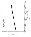
- Figure 4 shows the effect of Increasing temperature on the inverse of electrical conductivity (resistivity) while Figure 5 shows the effect of increasing temperature on the Seebeck coefficient of the compound KPb 8 BiTe 10 . Increasing the temperature results in a larger Seebeck coefficient.
- the isostructural compounds of the present invention may be doped with selected impurities to produce P-type and N-type conductors having improved thermoelectric properties such as enhanced Seebeck coefficients and figures of merit (zT).
- zT enhanced Seebeck coefficients and figures of merit
- an enhanced N-type conductor one atom is replaced by another atom having more valence electrons, wherein the extra electrons are not needed for bonding and are free to move throughout the crystal.
- a P-type conductor is formed when an atom in the isostructural compound is replaced by another atom with fewer electrons, leaving a bond vacant wherein this shortage is referred to as a hole.
- the compounds of the present invention always exhibit P-type conductivity when the compounds are prepared by high temperature reaction with stoichlometric amounts of the constituent components.
- Enhanced P-type semiconductors can be produced from the compounds of the present invention.
- doping with one electron deficient elements such as Group IV elements (Ge, Sn, Pb) and Group III elements (Al, Ga, In, Tl), respectively, may produce more hole carriers which give rise to improved electrical properties.
- the isostructural components of the present invention can be used to produce N-type semiconductor materials by doping with various impurities.
- Isovalent anionic dopants where S or Se is substituted for Te and S for Se may be used In about less than 1 atomic percent.
- Other examples of compounds that can be used for doping are the metal halides SbX 3 , BiX 3 , and Hg 2 Cl 2 , DX 2 where X is selected from the group consisting essentially of chlorine, bromine, iodine and mixtures thereof and D is selected from the group consisting essentially of chromium, manganese, iron, cobalt, nickel, copper, zinc, magnesium and mixtures thereof.
- SbX 3 , BiX 3 , and Hg 2 Cl 2 , DX 2 where X is selected from the group consisting essentially of chlorine, bromine, iodine and mixtures thereof and D is selected from the group consisting essentially of chromium, manganese, iron, cobalt, nickel, copper,
- Doping of the isostructural compounds of the present invention can be achieved by introducing the desired amount of dopant during synthesis. Stoichiometric amounts of the dopant can be added to the starting materials. Alternately, the compounds of the present invention can be doped by co-melting the desired compound and the dopant and recooling the new mixture. The amount of dopant preferably ranges from 0.0001 % to 4% by weight.
- the isostructural compounds of the present invention may be used in a thermoelectrical conversion process in a thermoelectric conversion device.
- the thermoelectric conversion process using the isostructural compounds of the present invention may take any appropriate form, such as any known device and/or structure, as long as thermoelectric conversion principles are met.
- Such devices may be, but are not limited to, electrical power generators, heater, coolers, thermocouples, temperature sensors and radioisotope thermoelectric generators.
- Other thermoelectric devices that can be manufactured using the compounds of the present invention may be used in waste heat recovery systems, automobiles, remote power generators, temperature sensors and coolers for advanced electronic components such as field effect transistors, as non-limiting examples.
- the isostructural compounds of the present invention may take any number of appropriate shapes.
- the compounds may be used in a lump shape or they may be formed in the shape of a thin film by a growth method, vapor deposition, or other techniques known to those skilled in the art. Regardless of the shape, the isostructural compounds of the present invention have excellent conductivity and thermoelectric properties. TABLE 1.
Landscapes
- Chemical & Material Sciences (AREA)
- Engineering & Computer Science (AREA)
- Inorganic Chemistry (AREA)
- Materials Engineering (AREA)
- Organic Chemistry (AREA)
- Crystallography & Structural Chemistry (AREA)
- Metallurgy (AREA)
- Ceramic Engineering (AREA)
- Manufacturing & Machinery (AREA)
- Structural Engineering (AREA)
- Inorganic Compounds Of Heavy Metals (AREA)
- Organic Low-Molecular-Weight Compounds And Preparation Thereof (AREA)
- Conductive Materials (AREA)
- Addition Polymer Or Copolymer, Post-Treatments, Or Chemical Modifications (AREA)
- Dental Preparations (AREA)
- Heterocyclic Carbon Compounds Containing A Hetero Ring Having Oxygen Or Sulfur (AREA)
Abstract
Description
- Work on this invention was sponsored in part by the Office of Naval Research, Grants N00014-94-1-0935 and N00014-98-1-0443 and Defense Advanced Research Projects Agency Grant DAAG55-97-1-0184. The Government may have certain rights to the invention.
- This invention relates generally to new compounds exhibiting crystal lattice morphologies and, more particularly, to conductive compounds having NaCl-type cubic crystal lattice structures.
- Semiconductor materials are at the core of current technological infrastructure and continuing advancements. Various semiconductors enable many technologies. For example, Si and Ge enable high speed computing, GaAs, InSb and their derivatives enable optoelectronics and communication devices, Si and GaAs are the vital components of solar energy converters, GaN and GaAs alloys enable solid state lasers, Bi2Te3 alloys enable thermoelectric cooling, and PbS, PbSe and HgCdTe are used in medium and long wavelength radiation detection.
- Semiconductor materials used in solid state lasers, photovoltaic cells, optoelectronic devices and radiation detection, for example, must not only be excellent electronic conductors, but also have the appropriate energy band configuration or "band gap" for those applications. As more than one material is used in layers, the difference in the band gap between the various semiconductor materials used is also critical. For example, photovoltaic cells can use two semiconductor materials to produce a rectifying heterojunction. The advantages of utilizing this design include the ability to choose materials with properties appropriate for each component of the device and the reduced necessity for compromise with the property requirements of other components of the device. An example of this is the use of a wide band gap "window" semiconductor material as a barrier layer on a more narrow band gap "absorber" semiconductor material. The amount of radiation absorbed and therefore the electrical current generated in the device, increases with the decreasing band gap width, while the diffusion potential obtainable within the device, and therefore the electrical voltage generated in the device, increases with band gap width. Thus, the absorber material is chosen to maximize the solar radiation absorbed and affords a reasonable diffusion potential, while window material is chosen to absorb a minimum amount of solar radiation. Therefore, the closer the actual band gap to the desired, theoretical band gap of the semiconductor materials, the more efficient the photovoltaic cell. Many current semiconductor materials are limited in that they do not allow for fine adjustment of the band gap. Furthermore, some semiconductor materials contain volatile elements causing changes in the composition of the materials and consequently unwanted changes in the band gap.
- In thermoelectric devices, it is also critical to have semiconductor materials that have specific properties. Such devices may be used for heating, cooling, temperature stabilization, power generation and temperature sensing. Modern thermoelectric coolers typically include an array of thermocouples.
- Thermoelectric devices are essentially heat pumps and power generators which follow the laws of thermodynamics in the same manner as mechanical heat pumps, refrigerators, or any other apparatus used to transfer heat energy. The efficiency of a thermoelectric device is generally limited to its associated Carnot cycle efficiency reduced by a factor which is dependent upon the thermoelectric figure of merit (zT) of the materials used in fabrication of the thermoelectric device. The figure of merit represents the coupling between electrical and thermal effects in a material. The basic thermoelectric effects are the Seebeck and Peltier effects. The Seebeck effect is the phenomenon underlying the conversion of heat energy into electrical power and is used in thermoelectric power generation. The complementary effect, the Peltier effect, is the phenomenon used in thermoelectric refrigeration and is related to heat absorption accompanying the passage of current through the junction of two dissimilar materials.
- While thermoelectric materials such as alloys of Bi2Te3, PbTe and BiSb were developed thirty to forty years ago, the efficiency of such thermoelectric devices remains relatively low at approximately five to eight percent energy conversion efficiency.
- Therefore it would be desirable to have semiconductor materials that are not only good conductors but have a range of band gaps to fit a wide number of applications. It would be further desirable to have materials in which the band gaps could be adjusted to give the desired band gap for the appropriate application. These materials should also be thermal and chemically stable.
- Furthermore, it would be desirable to have thermoelectric materials that have a high thermoelectric figure of merit. Use of such materials would produce thermoelectric devices with high efficiencies.
- The present invention relates to new isostructural compounds having the general formula AnMmM'nQ2n+m where A is silver (Ag), M is selected from lead (Pb), tin (Sn), and mixtures thereof, M' is selected from bismuth (Bi), antimony (Sb) and mixtures thereof, and Q is selected from the group consisting essentially of sulfur (S), selenium (Se), or tellurium (Te) and mixtures thereof and where n = 1 and 10 ≤ m ≤ 20. These compounds possess an NaCl-type cubic lattice crystal structure where A, M and M' occupy the Na sites and Q occupies the Cl (chlorine) sites. This family of compounds combine isotropic morphology, an advantageous property for device processing, with low thermal conductivity and widely ranged electrical conductivity. Further, certain properties such as the electrical properties of the compounds can be controlled by varying the values for n and m. The isostructural compounds of the present invention are therefore good candidates for semiconductor applications in thermoelectronic devices, detectors, and photovoltaic cells, by way of non-limiting example.
- Additional objects, advantages, and features of the present invention will become apparent from the following description and appended claims, taken in conjunction with the accompanying drawings.
-
-
Figure 1 is an illustration of the crystal structure of AnPbmBinQ2n+m; -
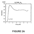
Figure 2A is a graph showing the infrared absorption spectrum of K2PbBi2Se5; -
Figure 2B is a graph showing the infrared absorption spectrum of KPb4BiSe6; -
Figure 2C is a graph showing the infrared absorption spectrum of KPb8BiSe10; -
Figure 2D is a graph showing the infrared absorption spectrum of PbSe; -
Figure 3 is an illustration showing a multispectral sensor with a two-materials stacked structure; -
Figure 4 is a graph showing the effect of increasing temperature on the resistivity of KPb8BiTe10; and -
Figure 5 is a graph showing the effect of increasing temperature on the Seebeck coefficient of KPb8BiTe10. - The present invention provides new isostructural compounds having the general formula AnMmM'nQ2n+m where A is silver (Ag), M is selected from lead (Pb), tin (Sn), and mixtures thereof, M' is selected from bismuth (Bi), antimony (Sb) and mixtures thereof, and Q is selected from the group consisting essentially of sulfur (S), selenium (Se), or tellurium (Te) and mixtures thereof.
- The variables n = 1 and 10 ≤ m ≤ 20. Preferably, n and m are integers.
- The compounds of the present invention can be synthesized utilizing at least two different groups of starting materials or from the pure elements themselves. According to one embodiment, the group of starting materials are A2Q, M, M' and Q and under another embodiment the group of starting materials are A2Q, M'2Q3. M and Q, wherein M and Q can be in the form of MQ as will be described below. In yet another embodiment, the pure elements, A, M, M' and Q, in the correct stoichiometric ratios can be used to synthesize the compounds of the present invention.
- A2Q can be prepared by reacting stoichiometric amounts of the elemental A (2 moles) with the elemental Q (1 mole) in liquid ammonia. When the reaction is complete, the ammonia is removed by evaporation at ambient temperature. The resulting product is dried and ground to give a fine homogeneous powder.
- M'2Q3 can be generally prepared by reacting stoichiometric amounts of elemental Bi or Sb (2 moles) and elemental Q (3 moles) at 800 °C for about 1-3 days at ambient pressure or optionally under a vacuum to reduce reaction times. Alternatively, bismuth telluride (Johnson Matthey/AESAR Group, Seabrook, NH) and bismuth selenide (Cerac, Inc, Milwaukee, WI) can be obtained commercially.
- MQ can be synthesized, for example, by thoroughly mixing stoichiometric amounts (1 mole each) of elemental Pb or Sn, and Q and loading the mixture into a quartz tube at a residual pressure of less than 10-4 Torr. The mixture is then heated to 800 °C over a 24 hour period and the temperature maintained for an additional 24 hours. The mixture is then cooled by quenching in water and the resulting ingot is crushed to a fine powder. The powder is then reloaded into a quartz tube and heated to 800 °C over a 24 hour period. The temperature of the mixture is maintained at 800 °C for an additional 24 hours and then slowly cooled to 300 °C at a rate of about 4 °C/hr and subsequently to 50 °C over about 6 hours. The resulting ingots are ground to a fine powder prior to synthesis of the compounds of the present invention.
- Upon forming each of the compounds included in the groups of starting materials, the isostructural compounds of the present invention are synthesized by thoroughly mixing and loading the chosen starting materials into a carbon coated quartz or capped graphite tube at a residual pressure less than 10-4 Torr, i.e., either the group of A2Q, M metal, M' metal and elemental Q or the group A2Q, M'2Q3 and MQ. The mixture is heated to 700 °C at a rate of about 30 °C/hr. After maintaining the temperature at 700 °C for approximately 3 days, the mixture is cooled to 300 °C at a rate of 5 °C/hr followed by cooling to 50 °C in about 12 hours. The resulting product is washed with degassed dimethylformamide and water in a nitrogen atmosphere. After further washing with diethyl ether and subsequent drying, the isostructural compounds of the present invention are obtained as shiny black chunks exhibiting the above described cubic phase.
- The compounds of the present invention can also be synthesized from the pure elements. The appropriate elements for the desired compound, A, M, M' and Q, are mixed together in the correct stoichiometric ratios and sealed in a quartz tube under vacuum, i.e., < 10-3 Torr. The mixture is then heated in a direct flame until molten. Subsequent cooling of the melt yields the corresponding compound. To synthesize KSnBiSe3, by way of non-inventive example, 0.01 mole (0.39g) of potassium, 0.01 mole (1.18 g) tin, 0.01 mole (2.09g) bismuth and 0.03 mole (2.37g) of selenium were mixed, placed in a quartz tube and sealed under vacuum at <10-3 Torr. The mixture was heated in a direct flame until molten and subsequently cooled to yield the desired product, KSnBiSe3.
- As noted above, the isostructural compounds of the present invention have a cubic crystal lattice structure of the same type as NaCl, wherein the cations (or metals) occupy the Na sites and the anions occupy the Cl sites. The cations, although differing in charge, are similar in size and tend to become randomly dispersed throughout the structure as shown in
Figure 1 . This cubic crystal structure is independent of the values for n and m and depends only on the elements selected to form the isostructural compounds. A property of this cubic structure of the compounds of the present invention is a morphology of low anisotropy which is desirable for fabricating electronic and optical devices, by way of non-limiting example. The cubic structure also gives rise to relatively high carrier mobilities and ease of crystal growth and processing. The compounds of the present invention also have relatively high melting point temperatures which are considered to be indicative of a high degree of structural stability. The melting temperatures of a significant number of the sample compounds of the present invention are greater than 850°C (Table 1). - The isostructural compounds of the present invention include band gaps which are tunable. By "band gaps" it is meant that there is an energy difference between the highest occupied electron state and the lowest unoccupied electron state in the isostructural compounds. Further, by "tunable" it is meant that this energy difference can be manipulated to obtain the desired band gap. One way of tuning the band gaps of isostructural compounds is by varying the values of n and m (Table 1). For example, the band gap of KPbBiSe3 (n=1, m=1) was measured at -0.60 eV which is in the desirable range for IR radiation detection. The compounds K2PbBizS5 (n=2, m=1) and KPb2BiS4 (n=1, m=2) have optical band gaps of 1.1 and 0.76 eV respectively- Depending on the values for n and m in AnMmM'nQ2n+m a relatively wide range of band-gaps is possible, i.e., from about 0.05 eV to 1.55 eV. Band gap values for other representative isostructural compounds are given in Table 1. Infrared spectra showing the band-gap transition are shown in
Figures 2A-C . For comparison purposes, the infrared spectrum for PbSe, which is commonly used as an IR detector and has an NaCl-type cubic crystal lattice structure, is shown inFigure 2D . - Another way of tuning the band gaps of isostructural compounds is by selecting certain cations and anions for A and Q, respectively. For example, if Se is chosen for Q and K is chosen for A, the isostructural compound KPb2BiSe4 has a band gap of 0.66 eV. If Q is changed from Se to Te, the corresponding compound KPb2BiTe4 has a band gap of less than 0.4 eV (Table 1). Depending on the application, appropriate band gaps can be chosen which would correspond to certain members of each family. One member of the family may be more appropriate for long wavelength detection, while another may be appropriate for short wavelength detection such as is used by IR lasers.
- Yet another way of controlling the band gaps for the overall composition is by combining various individual isostructural compounds to form solid solutions of the type (Li,Na,K,Rb,Cs,Ag,Tl)n(Sn, Pb, Ge, Ca, Sr, Ba)m(Bi,Sb)n(S,Se,Te)2n+m. By "solid solutions" what is meant is a single, solid, homogenous crystalline phase containing two or more chemical species. A so-called solid solution would be made up of at least two distinct chemical species such as AnPbmBinSe2n+m and AnPbmBinTe2n+m where Q represents two different anions (Se and Te), or KnPbmBinQ2n+m and AgnPbmBinQ2n+m where A now represents two different cations (K, Ag), by way of non-limiting example. Alternatively, M and M' may be represented by more than one element to form a solid solution. Examples of such compounds are, but not limited to, AgPbBi0.75Sb0.25Te3, AgPbBi0.5Sb0.5Te3, AgPbBi0.75Sb0.25Te3, AgPb0.75Sn0.25BiTe3, AgPb0.5Sn0.5BiTe3, and AgPb0.25Sn0.75BiTe3. Additional non-limiting examples of solid solutions are given in Table 1.
- It will be appreciated that although fractional numbers are used for the mole ratios, they can be combined to give the integer value for n or m. For example, in AgPb0.75Sn0.25BiTe3, Pb + Sn represent M and their combined mole fractions are equal to 1, the value for m.
- While the n and m values in the pure isostructural compounds provide a coarse dial to control band-gap, the solid solutions give a fine dial for band gap engineering. For example, KPb2BiSe4 has a band gap of 0.66 eV while KPb2BiTe4 has a band gap of less than 0.40 eV (Table 1). Therefore, solid solutions KPb2BiSe3Te, KPb2BiSe2Te2 and KPb2BiSeTe3 will all have band gaps that fall somewhere between 0.66 and 0.40 eV. The formation of solid solutions with these compositions provides yet another means for tuning the band gap.
- The isostructural compounds of the present invention can be used in optical applications including, for example, infrared and near infrared detectors, lasers and photovoltaic cells such as solar cells by way of non-limiting example. In optical applications, at least two materials having different band gaps are layered together to give the desired optical properties. The isostructural compounds of the present invention have a wide range of band gaps that can be finely tuned to give optimal performance in such optical applications. In addition, the lattice structures are identical, allowing for superior lattice matching of the layers compared to the layering of two compounds with varying structures.
- The isostructural compounds of the present invention can also be used in multi-spectral sensors. Multi-spectral sensors (e.g. long wavelength and short wavelength) offer the possibility of improved clutter rejection and improved recognition range. The proper fusing of the information from each spectral band is key to the realization of these advantages. One such application is the two color, stacked, co-located, three terminal back-to-back diodes pixel. Two color, simultaneous integration HgCdTe back-to-back diodes staring IRFPAs have been produced. Love, P. et al., Proceedings of the IRIS Detectors Specialty Group Symposium, pp.169-186 (1995). The materials of the present invention are well suited for this multispectral configuration because they provide lattice matching over a wide range of n and m. For example, a non-inventive two-material stacked structure with KPb2BiSe4 (Eg=0.66 eV) and KPb8BiSe10 (Eg=0.35 eV) can be built either by vapor deposition techniques or by fusion bonding of two individual crystals as illustrated in
Figure 3 along with the respective lattice constants, a. Current approaches using HgCdTe solid solutions (comprising HgTe and CdTe) require the growth of heterojunctions, which then requires precise lattice matching. Current techniques result in a lattice mismatch as great as 4-6%, compromising the performance of the multispectral sensor. In contrast, the isostructural compounds of the present invention can be utilized as individual compounds and therefore should not require precise compositional control at the junction. The lattice mismatch using the isostructural compounds of the present invention is significantly less than 4-6 %. With KPb2BeSe4 and KPb8BiSe10 in a stacked structure the lattice mismatch is < 2% (Figure 3 ). - Another application for isostructural compounds of the present invention is in thermoelectric devices. Such devices may be used for heating, cooling, temperature stabilization, power generation and temperature sensing. Recently, significant advances in the synthesis and design of new systems such as in filled skutterudites and quantum well structures provided new hope that high performance thermoelectric materials may be attainable. While the efficiency of thermoelectric coolers operating near room temperature is only about 10% of Carnot efficiency, the thermodynamics of thermoelectric cooling suggests that achieving close to 100% of Carnot efficiency is possible employing the isostructural compounds of the present invention.
- Thermoelectric devices are essentially heat pumps and power generators which follow the laws of thermodynamics in the same manner as mechanical heat pumps, refrigerators, or any other apparatus used to transfer heat energy. The principal difference is that thermoelectric devices function with solid state electrical components (thermocouples) as compared to more traditional mechanical/fluid heating and cooling components. An efficient thermoelectric device is fabricated from two materials, one N-type and the other a P-type conductor. Each material is separately chosen to optimize the figure of merit, zT, where zT = (S2σ/κ)T; S is the thermopower or Seebeck coefficient (µV/K), σ the electrical conductivity (S/cm), κ the thermal conductivity (W/m-K) and T the temperature (K). Therefore, to obtain a thermoelectric material having a high thermoelectric performance, It Is desirable to select a material having a large Seebeck coefficient, S, a large electrical conductivity, σ, and a small thermal conductivity, κ.
- The isostructural compounds of the present invention i.e. compounds 8-14 have a high thermoelectric performance resulting from large Seebeck coefficients, large electrical conductivities and small thermal conductivities (Table 1). The Seebeck coefficients of the compounds of the present invention range from about ±30 µV/k to about ±500 µV/k and the electrical conductivities from about 10 to about 7000 S/cm. Compounds 1-7, 15-75 are not part of the invention.
-
Figure 4 shows the effect of Increasing temperature on the inverse of electrical conductivity (resistivity) whileFigure 5 shows the effect of increasing temperature on the Seebeck coefficient of the compound KPb8BiTe10. Increasing the temperature results in a larger Seebeck coefficient. - The isostructural compounds of the present invention may be doped with selected impurities to produce P-type and N-type conductors having improved thermoelectric properties such as enhanced Seebeck coefficients and figures of merit (zT). In an enhanced N-type conductor, one atom is replaced by another atom having more valence electrons, wherein the extra electrons are not needed for bonding and are free to move throughout the crystal. Alternatively, a P-type conductor is formed when an atom in the isostructural compound is replaced by another atom with fewer electrons, leaving a bond vacant wherein this shortage is referred to as a hole.
- The compounds of the present invention always exhibit P-type conductivity when the compounds are prepared by high temperature reaction with stoichlometric amounts of the constituent components. Enhanced P-type semiconductors can be produced from the compounds of the present invention. For the cationic sites of Bi or Sb (Group V) and Pb or Sn (Group IV), doping with one electron deficient elements such as Group IV elements (Ge, Sn, Pb) and Group III elements (Al, Ga, In, Tl), respectively, may produce more hole carriers which give rise to improved electrical properties.
- The isostructural components of the present invention can be used to produce N-type semiconductor materials by doping with various impurities. Isovalent anionic dopants, where S or Se is substituted for Te and S for Se may be used In about less than 1 atomic percent. Other examples of compounds that can be used for doping are the metal halides SbX3, BiX3, and Hg2Cl2, DX2 where X is selected from the group consisting essentially of chlorine, bromine, iodine and mixtures thereof and D is selected from the group consisting essentially of chromium, manganese, iron, cobalt, nickel, copper, zinc, magnesium and mixtures thereof. These are examples of compounds that can be used for doping and are in no way meant to be limiting. It should be appreciated by those skilled in the art that any dopant can be used to dope the isostructural compounds of the present invention to form enhanced P-type and N-type semiconductors.
- Doping of the isostructural compounds of the present invention can be achieved by introducing the desired amount of dopant during synthesis. Stoichiometric amounts of the dopant can be added to the starting materials. Alternately, the compounds of the present invention can be doped by co-melting the desired compound and the dopant and recooling the new mixture. The amount of dopant preferably ranges from 0.0001 % to 4% by weight.
- The isostructural compounds of the present invention may be used in a thermoelectrical conversion process in a thermoelectric conversion device. The thermoelectric conversion process using the isostructural compounds of the present invention may take any appropriate form, such as any known device and/or structure, as long as thermoelectric conversion principles are met. Such devices may be, but are not limited to, electrical power generators, heater, coolers, thermocouples, temperature sensors and radioisotope thermoelectric generators. Other thermoelectric devices that can be manufactured using the compounds of the present invention may be used in waste heat recovery systems, automobiles, remote power generators, temperature sensors and coolers for advanced electronic components such as field effect transistors, as non-limiting examples.
- The isostructural compounds of the present invention may take any number of appropriate shapes. The compounds may be used in a lump shape or they may be formed in the shape of a thin film by a growth method, vapor deposition, or other techniques known to those skilled in the art. Regardless of the shape, the isostructural compounds of the present invention have excellent conductivity and thermoelectric properties.
TABLE 1. Compound Number n m Lattice Parameter (Å) Band Gap (eV) Melting Point (°C) κ a
(W/m-K)σ b
(S/cm)Sc
(µV/K)AgPbSIS3 1 1 1 5.753 0.54 >910 1.3 25 -160 AgPbBISe3 2 1 1 5.955 0.48 >920 1.0 67 -130 AgPbBiTe3 3 1 1 6.28 0.28 >900 1.15 300 -40 AgPbSbTe3 4 1 1 AgSnBiTe3 5 1 1 6.1639 AgPb2BiTe4 6 1 2 6.323 0.29 >850 1.2 180 -165 AgSn8BiSe10 7 1 8 5.926 >900 1.2 AgPb10BiS12 8 1 10 6.117 0.31 >900 1.1 AgPb10BiTe12 9 1 10 6.452 0.29 >850 1.1 AgPb10SbTe12 10 1 10 6.441 0.29 >850 1.0 AgPb10BiSe12 11 1 10 6.118 AgSn10BiS12 12 1 10 6.259 6700 AgPb10SbS12 13 1 10 5.905 300 AgPb13BiTe15 14 1 13 6.44 0.23 >800 1.6 AgPbBiTe2Se 15 1 1 6.185 1.3 400 -58 AgPbBiTe2.25Se0.75 16 1 1 6.19 1.1 150 -40 AgPbBiTe2.5Se0.5 17 1 1 1 6.247 1.6 77 -80 AgPbBiTe2.75Se0.25 18 1 1 6.274 1.15 133 -105 AgPbBi0.1Sb0.9Te3 19 1 1 AgPbBi0.05Sb0.05Te3 20 1 1 AgPbBi0.75Sb0.25Te3 21 1 1 6.261 0.268 29 -68 AgPbBi0.5Sb0.5Te3 22 1 1 6.261 0.27 3.91 250 AgPbBi0.25Sb0.75Te3 23 1 1 10 370 AgPb0.75Sn0.25BiTe3 24 1 1 0.18 59 -33 AgPb0.5Sn0.5BiTe3 25 1 1 310 AgPb0.25Sn0.75BiTe3 26 1 1 685 35 AgPbBiTe1.5Se1.5 27 1 1 6.13 AgPbBiTeSe2 28 1 1 6.078 AgPbBiTe0.5Se2.5 29 1 1 6.036 AgPbBie2.95Se0.05 30 1 1 6.223 -64 AgPbBiTe2.75Se0.25 31 1 1 6.245 666 -60 AgPbSb0.05Bi0.05Te3 32 1 1 0.37 430 KPb3BiS5 33 1 3 5.949 0.71 >850 K5Pb16Bi5S26 34 5 16 5.947 0.69 >850 KPb7BiS9 35 1 7 5.937 0.63 >850 KPb9BiS11 36 1 9 5.947 0.53 >850 K7PbBi7S16 37 7 1 5.975 1.02 >850 K5PbBi3S17 38 8 1 6.006 1.24 >850 K11PbBi11S23 39 1 1 6.009 1.30 >850 KPbBiSe3 40 1 1 6.182 0.6 1004 KPb2BiSe4 41 1 2 6.185 0.66 958 -515 KPb3BiSe5 42 1 3 6.175 0.64 977 40 KPb4BiSe6 43 1 4 6.154 0.56 1015 210 KPb5BiSe7 44 1 5 6.142 0.45 1035 500 KPb10BiSe12 45 1 10 6.112 0.32 >850 K2Pb23Bi2Se27 46 2 23 6.111 >850 K2PbBi2Se3 47 2 1 6.007 0.62 >900 K3PbBi3Se7 48 3 1 6.196 0.67 >900 KpbBiTe3 49 1 1 0.45 >900 <1.5 -125 KPb2BiTe4 50 1 2 6.469 <0.40 >900 1.7 700 -115 KPb3BiTe5 51 1 3 6.467 <0.38 >900 1.5 800 KPb4BiTe6 52 1 4 6.479 <0.37 >900 1.7 1000 -155 KPb5BiTe10 53 1 8 6.458 <0.36 >900 2.1 1100 -150 KPb10BiTe12 54 1 10 6.472 <0.36 >900 2.2 960 -145 KPb10BiSeS11 55 1 10 5.9815 KPb10BiSe3S9 56 1 10 6.0199 KPb10BiSe8S6 57 1 10 6.0635 KPb10BiSe9S3 58 1 10 6.1055 KPb10BiSe11S 59 1 10 6.1336 KPb10Bi0.75Sb0.25Te3Se5 60 1 10 6.3284 935 990 KPb10Bi0.5Sb0.5Te6Se6 61 1 10 6.3073 935 595 KPb10Bi0.75Sb0.25Te6Se6 62 1 10 6.2846 935 380 KPb6Sn2BiTe6Se6 63 1 10 6.2948 860 450 KPb6Sn4BiTe5Se6 64 1 10 6.27 860 40 KPb4Sn6BiTe6Se6 65 1 10 6.2544 860 100 KPb2Sn8BiTe6Se8 66 1 10 6.2094 860 360 KPbSbTe3 67 1 1 KPb5SbTe7 68 1 5 6.448 13 KPb10SbTe7 69 1 5 6.459 215 KsnBiTe3 70 1 1 150 KSn5BiTe7 71 1 5 230 KSn10BiTe12 72 1 10 6.292 990 KSnSbTe3 73 1 1 210 KSn5SbTe7 74 1 5 6.278 2630 KSn10SbTe12 75 1 10 6.363 4250 a Thermal conductivity
b Electrical conductivity at room temperature.
c Seebeck Coefficient at room temperature. - Although the present invention has been described in detail, it should be understood that various changes, substitutions and alterations can be made herein without departing from the scope to the invention.
Claims (14)
- A conductive material having the general formula AgnMmM'nQ2n+m, wherein:(a) M is at least one element selected from the group consisting of Pb and Sn,(b) M' is at least one element selected from the group consisting of Bi and Sb;(c) Q is at least one element selected from the group consisting of Se, Te and S; and(d) n = 1 , and 10 ≤ m ≤ 20.
- A conductive material according to Claim 1, wherein M is Pb, M' is Sb, and Q is Te.
- A conductive material according to Claim 2 additionally comprising a dopant.
- A semiconductor device comprising the conductive material of to any one of the claims 1 to 3.
- An infrared detector comprising the conductive material of to any one of the claims 1 to 3.
- A photovoltaic element comprising the conductive material of to any one of the claims I to 3.
- A thermoelectric device comprising the conductive material of to any one of the claims I to 3.
- A N-type conductive material comprising the conductive material according to claim 1 and a dopant.
- A conductive material according to Claim 8, wherein M is Pb, M' is Sb, and Q is Te.
- A P-type conductive material according to any of Claims 1-3.
- A semiconductor device comprising the conductive material of any one of the claims 8 to 10.
- An infrared detector comprising the conductive material of any one of the claims 8 to 10.
- A photovoltaic cell comprising the conductive material of any one of the claims 8 to 10.
- A thermoelectric device comprising the conductive material of any one of the claims 8 to 10.
Priority Applications (2)
| Application Number | Priority Date | Filing Date | Title |
|---|---|---|---|
| EP08012925A EP2009672A1 (en) | 1998-10-13 | 1999-10-13 | Conductive isostructural compounds |
| EP09003807A EP2068348B1 (en) | 1998-10-13 | 1999-10-13 | Conductive isostructural compounds |
Applications Claiming Priority (3)
| Application Number | Priority Date | Filing Date | Title |
|---|---|---|---|
| US10396198P | 1998-10-13 | 1998-10-13 | |
| US103961P | 1998-10-13 | ||
| PCT/US1999/023849 WO2000024040A2 (en) | 1998-10-13 | 1999-10-13 | Conductive isostructural compounds |
Related Child Applications (4)
| Application Number | Title | Priority Date | Filing Date |
|---|---|---|---|
| EP08012925A Division EP2009672A1 (en) | 1998-10-13 | 1999-10-13 | Conductive isostructural compounds |
| EP09003807A Division EP2068348B1 (en) | 1998-10-13 | 1999-10-13 | Conductive isostructural compounds |
| EP08012925.7 Division-Into | 2008-07-17 | ||
| EP09003807.6 Division-Into | 2009-03-17 |
Publications (3)
| Publication Number | Publication Date |
|---|---|
| EP1129473A2 EP1129473A2 (en) | 2001-09-05 |
| EP1129473A4 EP1129473A4 (en) | 2004-03-17 |
| EP1129473B1 true EP1129473B1 (en) | 2010-06-09 |
Family
ID=22297936
Family Applications (3)
| Application Number | Title | Priority Date | Filing Date |
|---|---|---|---|
| EP99968846A Expired - Lifetime EP1129473B1 (en) | 1998-10-13 | 1999-10-13 | Conductive isostructural compounds |
| EP09003807A Expired - Lifetime EP2068348B1 (en) | 1998-10-13 | 1999-10-13 | Conductive isostructural compounds |
| EP08012925A Withdrawn EP2009672A1 (en) | 1998-10-13 | 1999-10-13 | Conductive isostructural compounds |
Family Applications After (2)
| Application Number | Title | Priority Date | Filing Date |
|---|---|---|---|
| EP09003807A Expired - Lifetime EP2068348B1 (en) | 1998-10-13 | 1999-10-13 | Conductive isostructural compounds |
| EP08012925A Withdrawn EP2009672A1 (en) | 1998-10-13 | 1999-10-13 | Conductive isostructural compounds |
Country Status (7)
| Country | Link |
|---|---|
| US (2) | US6312617B1 (en) |
| EP (3) | EP1129473B1 (en) |
| AT (2) | ATE546826T1 (en) |
| AU (1) | AU2705800A (en) |
| CA (1) | CA2347429C (en) |
| DE (1) | DE69942491D1 (en) |
| WO (1) | WO2000024040A2 (en) |
Families Citing this family (51)
| Publication number | Priority date | Publication date | Assignee | Title |
|---|---|---|---|---|
| JP2003179243A (en) * | 2001-08-31 | 2003-06-27 | Basf Ag | Photovoltaic active material and battery containing the same |
| US6812395B2 (en) * | 2001-10-24 | 2004-11-02 | Bsst Llc | Thermoelectric heterostructure assemblies element |
| CN100452466C (en) * | 2003-09-12 | 2009-01-14 | 密歇根州州立大学托管委员会 | Thermoelectric material and its preparation method, thermoelectric element and method of generating electric current from thermal energy |
| US8481843B2 (en) * | 2003-09-12 | 2013-07-09 | Board Of Trustees Operating Michigan State University | Silver-containing p-type semiconductor |
| US8455751B2 (en) * | 2003-12-02 | 2013-06-04 | Battelle Memorial Institute | Thermoelectric devices and applications for the same |
| US20050139250A1 (en) * | 2003-12-02 | 2005-06-30 | Battelle Memorial Institute | Thermoelectric devices and applications for the same |
| CA2549826C (en) * | 2003-12-02 | 2014-04-08 | Battelle Memorial Institute | Thermoelectric devices and applications for the same |
| EP1721067B1 (en) | 2004-03-02 | 2010-01-06 | Rosemount, Inc. | Process device with improved power generation |
| US7591913B2 (en) * | 2004-04-06 | 2009-09-22 | Massachusetts Institute Of Technology | Thermoelectric properties by high temperature annealing |
| US8538560B2 (en) | 2004-04-29 | 2013-09-17 | Rosemount Inc. | Wireless power and communication unit for process field devices |
| US8145180B2 (en) | 2004-05-21 | 2012-03-27 | Rosemount Inc. | Power generation for process devices |
| US7465871B2 (en) | 2004-10-29 | 2008-12-16 | Massachusetts Institute Of Technology | Nanocomposites with high thermoelectric figures of merit |
| US8865995B2 (en) * | 2004-10-29 | 2014-10-21 | Trustees Of Boston College | Methods for high figure-of-merit in nanostructured thermoelectric materials |
| US9184364B2 (en) | 2005-03-02 | 2015-11-10 | Rosemount Inc. | Pipeline thermoelectric generator assembly |
| US7586033B2 (en) * | 2005-05-03 | 2009-09-08 | Massachusetts Institute Of Technology | Metal-doped semiconductor nanoparticles and methods of synthesis thereof |
| US7255846B2 (en) * | 2005-05-03 | 2007-08-14 | Massachusetts Institute Of Technology | Methods for synthesis of semiconductor nanocrystals and thermoelectric compositions |
| US7847179B2 (en) | 2005-06-06 | 2010-12-07 | Board Of Trustees Of Michigan State University | Thermoelectric compositions and process |
| US7952015B2 (en) * | 2006-03-30 | 2011-05-31 | Board Of Trustees Of Michigan State University | Pb-Te-compounds doped with tin-antimony-tellurides for thermoelectric generators or peltier arrangements |
| US20100111754A1 (en) * | 2006-07-12 | 2010-05-06 | Gm Global Technology Operations, Inc. | Potassium and Sodium Filled Skutterudites |
| US8188359B2 (en) | 2006-09-28 | 2012-05-29 | Rosemount Inc. | Thermoelectric generator assembly for field process devices |
| US20080289677A1 (en) * | 2007-05-25 | 2008-11-27 | Bsst Llc | Composite thermoelectric materials and method of manufacture |
| US20090084421A1 (en) * | 2007-09-28 | 2009-04-02 | Battelle Memorial Institute | Thermoelectric devices |
| BRPI0906885A2 (en) * | 2008-01-14 | 2019-09-24 | The Ohio State University Research Foundation | thermoelectric materials and devices and methods of manufacture and use of thermoelectric devices |
| WO2009132314A2 (en) * | 2008-04-24 | 2009-10-29 | Bsst Llc | Improved thermoelectric materials combining increased power factor and reduced thermal conductivity |
| JP5554328B2 (en) | 2008-06-17 | 2014-07-23 | ローズマウント インコーポレイテッド | RF adapter for field devices with intrinsically safe low voltage clamp circuit |
| EP2310918B1 (en) | 2008-06-17 | 2014-10-08 | Rosemount, Inc. | Rf adapter for field device with variable voltage drop |
| US8694060B2 (en) | 2008-06-17 | 2014-04-08 | Rosemount Inc. | Form factor and electromagnetic interference protection for process device wireless adapters |
| US8929948B2 (en) | 2008-06-17 | 2015-01-06 | Rosemount Inc. | Wireless communication adapter for field devices |
| WO2010120697A1 (en) * | 2009-04-13 | 2010-10-21 | The Ohio State University | Thermoelectric alloys with improved thermoelectric power factor |
| US8626087B2 (en) | 2009-06-16 | 2014-01-07 | Rosemount Inc. | Wire harness for field devices used in a hazardous locations |
| US9674976B2 (en) | 2009-06-16 | 2017-06-06 | Rosemount Inc. | Wireless process communication adapter with improved encapsulation |
| US10761524B2 (en) | 2010-08-12 | 2020-09-01 | Rosemount Inc. | Wireless adapter with process diagnostics |
| US8795545B2 (en) | 2011-04-01 | 2014-08-05 | Zt Plus | Thermoelectric materials having porosity |
| US9310794B2 (en) | 2011-10-27 | 2016-04-12 | Rosemount Inc. | Power supply for industrial process field device |
| US9362429B2 (en) | 2013-04-30 | 2016-06-07 | Alliance For Sustainable Energy, Llc | Photovoltaic semiconductor materials based on alloys of tin sulfide, and methods of production |
| CN103579486B (en) * | 2013-11-20 | 2016-08-10 | 遵义师范学院 | Potassium mixes bismuth-antimony system i.e. Bi85Sb15-xKx low-temperature thermoelectric material and preparation method thereof |
| WO2018080085A1 (en) * | 2016-10-31 | 2018-05-03 | 주식회사 엘지화학 | Chalcogenide compound, production method thereof and thermoelectric element comprising same |
| KR102094451B1 (en) * | 2016-10-31 | 2020-03-27 | 주식회사 엘지화학 | Chalcogen-containing compound, its preparation method and thermoelectric element comprising the same |
| KR102121434B1 (en) * | 2017-05-15 | 2020-06-10 | 주식회사 엘지화학 | Chalcogen-containing compound, its preparation method and thermoelectric element comprising the same |
| KR102123041B1 (en) * | 2017-06-07 | 2020-06-15 | 주식회사 엘지화학 | Chalcogen-containing compound, its preparation method and thermoelectric element comprising the same |
| KR102121436B1 (en) * | 2017-06-27 | 2020-06-10 | 주식회사 엘지화학 | Chalcogen-containing compound, its preparation method and thermoelectric element comprising the same |
| WO2019004613A1 (en) * | 2017-06-30 | 2019-01-03 | 주식회사 엘지화학 | Chalcogen compound, method for preparing same, and thermoelectric device comprising same |
| US11508865B2 (en) | 2017-07-17 | 2022-11-22 | Northwestern University | Copper halide chalcogenide semiconductor compounds for photonic devices |
| KR102138937B1 (en) * | 2017-09-29 | 2020-07-28 | 주식회사 엘지화학 | Chalcogen-containing compound, its preparation method and thermoelectric element comprising the same |
| WO2019066580A2 (en) * | 2017-09-29 | 2019-04-04 | 주식회사 엘지화학 | Chalcogen compound, method for preparing same, and thermoelectric element comprising same |
| JP7523027B2 (en) * | 2018-07-23 | 2024-07-26 | パナソニックIpマネジメント株式会社 | Thermoelectric conversion material and method for obtaining electric power using the thermoelectric conversion material |
| KR102573731B1 (en) | 2018-08-24 | 2023-08-31 | 주식회사 엘지화학 | Chalcogen-containing compound, its preparation method and thermoelectric element comprising the same |
| WO2020079872A1 (en) * | 2018-10-17 | 2020-04-23 | パナソニックIpマネジメント株式会社 | Thermoelectric conversion material and method for obtaining electrical power by using thermoelectric conversion material |
| WO2020079873A1 (en) * | 2018-10-17 | 2020-04-23 | パナソニックIpマネジメント株式会社 | Thermoelectric conversion material and method for obtaining electrical power by using thermoelectric conversion material |
| CN110106554A (en) * | 2019-06-14 | 2019-08-09 | 中国科学院新疆理化技术研究所 | Bromine selenium barium aluminium birefringece crystal and its preparation method and application |
| CN116281881B (en) * | 2023-03-24 | 2024-04-05 | 西安交通大学 | Bismuth telluride-based thermoelectric material, preparation method and application thereof |
Family Cites Families (27)
| Publication number | Priority date | Publication date | Assignee | Title |
|---|---|---|---|---|
| US2602095A (en) | 1950-06-03 | 1952-07-01 | Gen Electric | Thermoelectric device |
| US2728637A (en) | 1953-07-27 | 1955-12-27 | Du Pont | Ternary alkaline earth metal sulfides of titanium and their preparation |
| US2770528A (en) | 1954-03-15 | 1956-11-13 | Du Pont | Barium ferrous group metal ternary sulfides and their preparation |
| US2882468A (en) | 1957-05-10 | 1959-04-14 | Bell Telephone Labor Inc | Semiconducting materials and devices made therefrom |
| US2882467A (en) | 1957-05-10 | 1959-04-14 | Bell Telephone Labor Inc | Semiconducting materials and devices made therefrom |
| US3008797A (en) | 1957-10-10 | 1961-11-14 | Du Pont | Ternary selenides and tellurides of silver and antimony and their preparation |
| CH441507A (en) * | 1958-11-28 | 1968-01-15 | Siemens Ag | Semiconductor device with a mixed crystal as the semiconductor body |
| NL253488A (en) * | 1959-07-13 | |||
| NL265338A (en) * | 1960-06-03 | 1900-01-01 | ||
| NL278300A (en) * | 1961-06-16 | |||
| US3945855A (en) * | 1965-11-24 | 1976-03-23 | Teledyne, Inc. | Thermoelectric device including an alloy of GeTe and AgSbTe as the P-type element |
| JPS63251290A (en) * | 1987-04-08 | 1988-10-18 | Hitachi Ltd | Optical recording media, recording/playback methods, and their applications |
| US5368701A (en) * | 1993-06-11 | 1994-11-29 | Nec Research Institute, Inc. | Process for forming Zintl phases and the products thereof |
| US5610366A (en) | 1993-08-03 | 1997-03-11 | California Institute Of Technology | High performance thermoelectric materials and methods of preparation |
| US6069312A (en) | 1994-01-28 | 2000-05-30 | California Institute Of Technology | Thermoelectric materials with filled skutterudite structure for thermoelectric devices |
| US5708233A (en) | 1994-02-22 | 1998-01-13 | Kabushiki Kaisha Ohara | Thermoelectric semiconductor material |
| US5448109B1 (en) | 1994-03-08 | 1997-10-07 | Tellurex Corp | Thermoelectric module |
| JP3455588B2 (en) * | 1994-06-29 | 2003-10-14 | 浜松ホトニクス株式会社 | Photoelectric detector with cooling device and method of manufacturing the same |
| JP3092463B2 (en) | 1994-10-11 | 2000-09-25 | ヤマハ株式会社 | Thermoelectric material and thermoelectric conversion element |
| US5773829A (en) * | 1996-11-05 | 1998-06-30 | Iwanczyk; Jan S. | Radiation imaging detector |
| WO1998037587A1 (en) | 1997-02-21 | 1998-08-27 | Volvo Aero Corporation | A thermoelectric generator unit |
| US5936193A (en) * | 1997-05-09 | 1999-08-10 | Parise; Ronald J. | Nighttime solar cell |
| US6129673A (en) * | 1998-06-08 | 2000-10-10 | Advanced Monitors, Corp. | Infrared thermometer |
| US6103967A (en) | 1998-06-29 | 2000-08-15 | Tellurex Corporation | Thermoelectric module and method of manufacturing the same |
| US6313393B1 (en) | 1999-10-21 | 2001-11-06 | Battelle Memorial Institute | Heat transfer and electric-power-generating component containing a thermoelectric device |
| DE19955788A1 (en) | 1999-11-19 | 2001-05-23 | Basf Ag | Thermoelectrically active materials and generators containing them |
| US8481843B2 (en) * | 2003-09-12 | 2013-07-09 | Board Of Trustees Operating Michigan State University | Silver-containing p-type semiconductor |
-
1999
- 1999-10-11 US US09/416,165 patent/US6312617B1/en not_active Ceased
- 1999-10-13 CA CA002347429A patent/CA2347429C/en not_active Expired - Fee Related
- 1999-10-13 EP EP99968846A patent/EP1129473B1/en not_active Expired - Lifetime
- 1999-10-13 DE DE69942491T patent/DE69942491D1/en not_active Expired - Lifetime
- 1999-10-13 EP EP09003807A patent/EP2068348B1/en not_active Expired - Lifetime
- 1999-10-13 EP EP08012925A patent/EP2009672A1/en not_active Withdrawn
- 1999-10-13 AT AT09003807T patent/ATE546826T1/en active
- 1999-10-13 AT AT99968846T patent/ATE470951T1/en not_active IP Right Cessation
- 1999-10-13 AU AU27058/00A patent/AU2705800A/en not_active Abandoned
- 1999-10-13 WO PCT/US1999/023849 patent/WO2000024040A2/en not_active Ceased
-
2003
- 2003-11-06 US US10/703,026 patent/USRE39640E1/en not_active Expired - Lifetime
Also Published As
| Publication number | Publication date |
|---|---|
| CA2347429A1 (en) | 2000-04-27 |
| CA2347429C (en) | 2004-02-24 |
| ATE470951T1 (en) | 2010-06-15 |
| EP1129473A4 (en) | 2004-03-17 |
| ATE546826T1 (en) | 2012-03-15 |
| EP2068348B1 (en) | 2012-02-22 |
| EP2009672A1 (en) | 2008-12-31 |
| EP1129473A2 (en) | 2001-09-05 |
| DE69942491D1 (en) | 2010-07-22 |
| US6312617B1 (en) | 2001-11-06 |
| USRE39640E1 (en) | 2007-05-22 |
| WO2000024040A2 (en) | 2000-04-27 |
| WO2000024040A3 (en) | 2000-07-20 |
| EP2068348A1 (en) | 2009-06-10 |
| AU2705800A (en) | 2000-05-08 |
Similar Documents
| Publication | Publication Date | Title |
|---|---|---|
| EP2068348B1 (en) | Conductive isostructural compounds | |
| US7592535B2 (en) | Silver-containing thermoelectric compounds | |
| US8481843B2 (en) | Silver-containing p-type semiconductor | |
| US5900071A (en) | Superlattice structures particularly suitable for use as thermoelectric materials | |
| JP6164627B2 (en) | New compound semiconductors and their utilization | |
| US5747728A (en) | Advanced thermoelectric materials with enhanced crystal lattice structure and methods of preparation | |
| JP2011516370A (en) | NOVEL THERMOELECTRIC CONVERSION MATERIAL, MANUFACTURING METHOD THEREOF, AND THERMOELECTRIC CONVERSION DEVICE USING THE SAME | |
| US4491679A (en) | Thermoelectric materials and devices made therewith | |
| US5769943A (en) | Semiconductor apparatus utilizing gradient freeze and liquid-solid techniques | |
| KR20200027754A (en) | SnSe2 BASED THERMOELECTRIC MATERIAL AND PRODUCING METHOD OF THE SAME | |
| KR102113260B1 (en) | Compound semiconductors having high performance and preparation method thereof | |
| US3310493A (en) | Halogen doped bi2te3-bi2se3-as2se3 thermoelectric composition | |
| EP3416204B1 (en) | Novel compound semiconductor and use thereof | |
| Oosawa et al. | PbBi/sub 2/Te/sub 4/and PbBi/sub 4/Te/sub 7/, thermoelectric materials in the system of Pb-Bi-Te | |
| Shah et al. | Effects of Pb doping on the thermoelectric properties of Tl8. 67PbxSb1. 33-xTe6 materials | |
| Kim | Exploratory synthesis and characterization of new multinary bismuth chalcogenides related by phase homologies |
Legal Events
| Date | Code | Title | Description |
|---|---|---|---|
| PUAI | Public reference made under article 153(3) epc to a published international application that has entered the european phase |
Free format text: ORIGINAL CODE: 0009012 |
|
| 17P | Request for examination filed |
Effective date: 20010514 |
|
| AK | Designated contracting states |
Kind code of ref document: A2 Designated state(s): AT BE CH CY DE DK ES FI FR GB GR IE IT LI LU MC NL PT SE |
|
| AX | Request for extension of the european patent |
Free format text: AL;LT;LV;MK PAYMENT 20010514;RO;SI |
|
| A4 | Supplementary search report drawn up and despatched |
Effective date: 20040203 |
|
| RIC1 | Information provided on ipc code assigned before grant |
Ipc: 7C 01G 29/00 B Ipc: 7C 01G 30/00 B Ipc: 7C 30B 29/46 B Ipc: 7C 30B 11/00 B Ipc: 7H 01L 35/18 B Ipc: 7H 01L 35/16 B Ipc: 7H 01L 31/032 B Ipc: 7H 01L 29/24 B Ipc: 7H 01L 21/00 A |
|
| 17Q | First examination report despatched |
Effective date: 20040422 |
|
| GRAP | Despatch of communication of intention to grant a patent |
Free format text: ORIGINAL CODE: EPIDOSNIGR1 |
|
| GRAS | Grant fee paid |
Free format text: ORIGINAL CODE: EPIDOSNIGR3 |
|
| GRAA | (expected) grant |
Free format text: ORIGINAL CODE: 0009210 |
|
| AK | Designated contracting states |
Kind code of ref document: B1 Designated state(s): AT BE CH CY DE DK ES FI FR GB GR IE IT LI LU MC NL PT SE |
|
| AX | Request for extension of the european patent |
Extension state: MK |
|
| REG | Reference to a national code |
Ref country code: CH Ref legal event code: EP |
|
| REG | Reference to a national code |
Ref country code: IE Ref legal event code: FG4D |
|
| REF | Corresponds to: |
Ref document number: 69942491 Country of ref document: DE Date of ref document: 20100722 Kind code of ref document: P |
|
| REG | Reference to a national code |
Ref country code: NL Ref legal event code: VDEP Effective date: 20100609 |
|
| PG25 | Lapsed in a contracting state [announced via postgrant information from national office to epo] |
Ref country code: SE Free format text: LAPSE BECAUSE OF FAILURE TO SUBMIT A TRANSLATION OF THE DESCRIPTION OR TO PAY THE FEE WITHIN THE PRESCRIBED TIME-LIMIT Effective date: 20100609 |
|
| PG25 | Lapsed in a contracting state [announced via postgrant information from national office to epo] |
Ref country code: FI Free format text: LAPSE BECAUSE OF FAILURE TO SUBMIT A TRANSLATION OF THE DESCRIPTION OR TO PAY THE FEE WITHIN THE PRESCRIBED TIME-LIMIT Effective date: 20100609 Ref country code: AT Free format text: LAPSE BECAUSE OF FAILURE TO SUBMIT A TRANSLATION OF THE DESCRIPTION OR TO PAY THE FEE WITHIN THE PRESCRIBED TIME-LIMIT Effective date: 20100609 |
|
| PG25 | Lapsed in a contracting state [announced via postgrant information from national office to epo] |
Ref country code: CY Free format text: LAPSE BECAUSE OF NON-PAYMENT OF DUE FEES Effective date: 20100609 |
|
| PG25 | Lapsed in a contracting state [announced via postgrant information from national office to epo] |
Ref country code: NL Free format text: LAPSE BECAUSE OF FAILURE TO SUBMIT A TRANSLATION OF THE DESCRIPTION OR TO PAY THE FEE WITHIN THE PRESCRIBED TIME-LIMIT Effective date: 20100609 |
|
| PG25 | Lapsed in a contracting state [announced via postgrant information from national office to epo] |
Ref country code: PT Free format text: LAPSE BECAUSE OF FAILURE TO SUBMIT A TRANSLATION OF THE DESCRIPTION OR TO PAY THE FEE WITHIN THE PRESCRIBED TIME-LIMIT Effective date: 20101011 Ref country code: BE Free format text: LAPSE BECAUSE OF FAILURE TO SUBMIT A TRANSLATION OF THE DESCRIPTION OR TO PAY THE FEE WITHIN THE PRESCRIBED TIME-LIMIT Effective date: 20100609 |
|
| PG25 | Lapsed in a contracting state [announced via postgrant information from national office to epo] |
Ref country code: IT Free format text: LAPSE BECAUSE OF FAILURE TO SUBMIT A TRANSLATION OF THE DESCRIPTION OR TO PAY THE FEE WITHIN THE PRESCRIBED TIME-LIMIT Effective date: 20100609 |
|
| PLBE | No opposition filed within time limit |
Free format text: ORIGINAL CODE: 0009261 |
|
| STAA | Information on the status of an ep patent application or granted ep patent |
Free format text: STATUS: NO OPPOSITION FILED WITHIN TIME LIMIT |
|
| PG25 | Lapsed in a contracting state [announced via postgrant information from national office to epo] |
Ref country code: DK Free format text: LAPSE BECAUSE OF FAILURE TO SUBMIT A TRANSLATION OF THE DESCRIPTION OR TO PAY THE FEE WITHIN THE PRESCRIBED TIME-LIMIT Effective date: 20100609 |
|
| PG25 | Lapsed in a contracting state [announced via postgrant information from national office to epo] |
Ref country code: GR Free format text: LAPSE BECAUSE OF FAILURE TO SUBMIT A TRANSLATION OF THE DESCRIPTION OR TO PAY THE FEE WITHIN THE PRESCRIBED TIME-LIMIT Effective date: 20100910 Ref country code: MC Free format text: LAPSE BECAUSE OF NON-PAYMENT OF DUE FEES Effective date: 20101031 |
|
| REG | Reference to a national code |
Ref country code: CH Ref legal event code: PL |
|
| GBPC | Gb: european patent ceased through non-payment of renewal fee |
Effective date: 20101013 |
|
| REG | Reference to a national code |
Ref country code: DE Ref legal event code: R097 Ref document number: 69942491 Country of ref document: DE Effective date: 20110309 |
|
| PG25 | Lapsed in a contracting state [announced via postgrant information from national office to epo] |
Ref country code: CH Free format text: LAPSE BECAUSE OF NON-PAYMENT OF DUE FEES Effective date: 20101031 Ref country code: FR Free format text: LAPSE BECAUSE OF NON-PAYMENT OF DUE FEES Effective date: 20101102 Ref country code: LI Free format text: LAPSE BECAUSE OF NON-PAYMENT OF DUE FEES Effective date: 20101031 |
|
| REG | Reference to a national code |
Ref country code: FR Ref legal event code: ST Effective date: 20110630 |
|
| PG25 | Lapsed in a contracting state [announced via postgrant information from national office to epo] |
Ref country code: GB Free format text: LAPSE BECAUSE OF NON-PAYMENT OF DUE FEES Effective date: 20101013 |
|
| PG25 | Lapsed in a contracting state [announced via postgrant information from national office to epo] |
Ref country code: IE Free format text: LAPSE BECAUSE OF NON-PAYMENT OF DUE FEES Effective date: 20101013 |
|
| PG25 | Lapsed in a contracting state [announced via postgrant information from national office to epo] |
Ref country code: LU Free format text: LAPSE BECAUSE OF NON-PAYMENT OF DUE FEES Effective date: 20101013 |
|
| PG25 | Lapsed in a contracting state [announced via postgrant information from national office to epo] |
Ref country code: ES Free format text: LAPSE BECAUSE OF FAILURE TO SUBMIT A TRANSLATION OF THE DESCRIPTION OR TO PAY THE FEE WITHIN THE PRESCRIBED TIME-LIMIT Effective date: 20100920 |
|
| PGFP | Annual fee paid to national office [announced via postgrant information from national office to epo] |
Ref country code: DE Payment date: 20131029 Year of fee payment: 15 |
|
| REG | Reference to a national code |
Ref country code: DE Ref legal event code: R119 Ref document number: 69942491 Country of ref document: DE |
|
| PG25 | Lapsed in a contracting state [announced via postgrant information from national office to epo] |
Ref country code: DE Free format text: LAPSE BECAUSE OF NON-PAYMENT OF DUE FEES Effective date: 20150501 |