EP1128460B1 - Dual mode band-pass filter - Google Patents
Dual mode band-pass filter Download PDFInfo
- Publication number
- EP1128460B1 EP1128460B1 EP01101079A EP01101079A EP1128460B1 EP 1128460 B1 EP1128460 B1 EP 1128460B1 EP 01101079 A EP01101079 A EP 01101079A EP 01101079 A EP01101079 A EP 01101079A EP 1128460 B1 EP1128460 B1 EP 1128460B1
- Authority
- EP
- European Patent Office
- Prior art keywords
- pass filter
- dual mode
- metallic film
- band
- mode band
- Prior art date
- Legal status (The legal status is an assumption and is not a legal conclusion. Google has not performed a legal analysis and makes no representation as to the accuracy of the status listed.)
- Expired - Lifetime
Links
Images


Classifications
-
- H—ELECTRICITY
- H01—ELECTRIC ELEMENTS
- H01P—WAVEGUIDES; RESONATORS, LINES, OR OTHER DEVICES OF THE WAVEGUIDE TYPE
- H01P7/00—Resonators of the waveguide type
- H01P7/08—Strip line resonators
-
- H—ELECTRICITY
- H01—ELECTRIC ELEMENTS
- H01P—WAVEGUIDES; RESONATORS, LINES, OR OTHER DEVICES OF THE WAVEGUIDE TYPE
- H01P7/00—Resonators of the waveguide type
- H01P7/08—Strip line resonators
- H01P7/082—Microstripline resonators
-
- H—ELECTRICITY
- H01—ELECTRIC ELEMENTS
- H01P—WAVEGUIDES; RESONATORS, LINES, OR OTHER DEVICES OF THE WAVEGUIDE TYPE
- H01P1/00—Auxiliary devices
- H01P1/20—Frequency-selective devices, e.g. filters
- H01P1/201—Filters for transverse electromagnetic waves
- H01P1/203—Strip line filters
- H01P1/20327—Electromagnetic interstage coupling
- H01P1/20354—Non-comb or non-interdigital filters
- H01P1/20381—Special shape resonators
-
- H—ELECTRICITY
- H01—ELECTRIC ELEMENTS
- H01P—WAVEGUIDES; RESONATORS, LINES, OR OTHER DEVICES OF THE WAVEGUIDE TYPE
- H01P7/00—Resonators of the waveguide type
- H01P7/08—Strip line resonators
- H01P7/084—Triplate line resonators
Definitions
- the present invention relates to a dual mode band-pass filter for use in, e.g., a communication equipment operating in the range of the microwave band to the milliwave band.
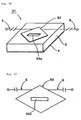
- FIGS. 48 and 49 are schematic plan views illustrating conventional dual mode band-pass filters, respectively.
- a circular conductive film 201 is formed on a dielectric substrate (not shown).
- Input-output coupling circuits 202 and 203 are coupled to the conductive film 201 so as to form an angle of 90° to each other.
- a tip-open stub 204 is formed on the conductive film 201 at the position thereof forming a central angle of 45° to the input-output coupling circuit 203.
- the band-pass filter 200 is configured so as to operate as a dual mode band-pass filter.
- a substantially square conductive film 211 is formed on a dielectric substrate.
- Input-output coupling circuits 212 and 213 are connected to the conductive film 211 so as to form an angle of 90° to each other.
- the corner of the conductive film 211 in the position thereof forming an angle of 135° with respect to the input-output coupling circuit 213 is cut away.
- the resonance frequencies in two resonance modes are made different from each other by the formed the cut portion 211a, so that the two resonance modes are coupled to each other.
- the band-pass filter 210 can be operated as a dual mode band-pass filter.
- a dual mode band-pass filter which contains a ring-shape conductive film instead of the circular conductive film (Japanese Unexamined Patent Application Publication No. 9-139612 and No. 9-162610, and so forth).
- a dual mode filter is disclosed, in which a ring-shaped ring transmission line is used, input-output coupling circuits are arranged so as to form a central angle of 90° similarly to the dual mode band-pass filter 200 shown in FIG. 48, and a tip-open stub is provided in a part of the ring transmission line.
- Japanese Unexamined Patent Application Publication No. 6-112701 discloses a dual mode band-pass filter which uses a ring transmission line similar to the above-mentioned transmission line.
- a ring resonator is formed in which a ring conductive film 222 is formed on a dielectric substrate.
- four terminals 223 to 226 are formed on the ring conductive film 222 so as to form an angle of 90° to each other with respect to the center of the ring conductive film 222.
- Two of the four terminals arranged at the positions forming an angle of 90° to each other with respect to the center of the ring conductive film are connected to input-output coupling circuits 227 and 228, respectively.
- the remaining two terminals 225 and 226 are connected to each other via a feedback circuit 230.
- a two step band-pass filter can be formed by forming one conductive film pattern. Accordingly, the band-pass filter can be miniaturized.
- the dual mode band-pass filters each have the configuration in which the input-output coupling circuits, separated from each other by an particular angle, are coupled to each other in the circular or square conductive film pattern. Therefore, the dual mode band-pass filters have the disadvantage that the coupling degree cannot be increased, and a wide pass band can not be attained.
- the conductive film 201 is restricted substantially onto a circular shape.
- the conductive film 211 is also limited to a substantially square shape. There is the problem that the design flexibility is low.
- Dual mode band-pass filters 221 using such a ring resonator as described in Japanese Unexamined Patent Application Publication Nos. 9-139612 and 9-162610 have the problem that it is difficult to enhance the coupling degree, and the shape and size of the ring resonator are restricted.
- the coupling degree is controlled, and the band-width can be widened by use of the feedback circuit 230.
- the feedback circuit 230 is required.
- the shape and size of the ring resonator is limited to a ring-shape, so that the design flexibility becomes low.
- EP 0 571 777 A1 describes a strip dual mode loop resonator having a loop-shaped strip line with a pair of straight strip lines arranged in parallel. Microwaves transferred from an input strip line to the loop-shaped strip line results in a reflection of the microwave in the straight strip lines of the loop-shaped strip line to produce reflected microwaves circulated in opposite directions. Thereafter, the reflected waves are resonated and filtered in dual mode in the loop-shaped strip line and provided to an outer strip line.
- EP-A-0 509 636 discloses a dual mode microstrip resonator usable in the design of microwave communication filters.
- the substantially square resonator provides paths for a pair of orthogonal signals which are coupled together using a perturbation located in at least one corner of the resonator.
- the present invention provides a dual mode band-pass filter which comprises a dielectric substrate having first and second main faces, a metallic film having an opening for coupling two resonance modes and formed in the first main face of the dielectric substrate or inside of the dielectric substrate, at least one ground electrode formed on the second main face of the dielectric substrate or inside of the dielectric substrate, so as to be opposed to the metallic film through a dielectric layer, and a pair of input-output coupling circuits connected to different parts of the metallic film.
- one of the two resonance modes that is, one propagated in parallel to the imaginary straight line passing through the connection points at which a pair of the input-output coupling circuits are connected to the metallic film, and the other propagated perpendicularly to the imaginary line, is affected by the opening so that the resonance frequency is varied.
- the opening is formed so as to exert an influence over the resonance current of one of the resonance modes whereby the one resonance mode can be coupled to the other resonance mode.
- the opening causes the two resonance modes to be coupled to each other, and the filter can be operated as a dual mode band-pass filter.
- the opening has a shape containing a long-size direction and a short-size direction.
- the plan shape of the opening is a rectangle, an ellipse, or a shape comprising a rectangle or ellipse having a bent part thereof elongating in a direction intersecting the long-size direction.
- the plan shape of the opening is a rectangle, a rhombus, a regular polygon, a circle, or an ellipse.
- Plural openings may be formed.
- the metallic film is formed on the first main face of the dielectric substrate, and the ground electrode is formed on the second main face.
- the metallic film is formed on a height level inside of the dielectric substrate, and the ground electrodes are formed on the first and second main faces of the dielectric substrate, whereby the band-pass filter has a tri-plate structure.
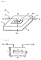
- FIG. 1 is a perspective view of a dual mode band-pass filter according to a first embodiment of the present invention.
- FIG. 2 is a schematic plan view of the dual mode band-pass filter;
- a dual mode band-pass filter 1 contains a rectangular sheet dielectric substrate 2.
- the dielectric substrate 2 is made of a fluororesin having a dielectric constant ⁇ r of 2.58.
- dielectric materials for forming the dielectric substrate appropriate dielectric materials such as BaO-Al 2 O 3 -SiO 2 type ceramics or the like can be used, in addition to the fluororesin.
- the thickness of the above-described dielectric substrate 2 has no particular limitations. In this embodiment, the thickness is set at 350 ⁇ m.
- a metallic film 3 is formed on the upper face 2a of the dielectric substrate 2 to produce a resonator.
- the metallic film 3 is formed in a partial area on the dielectric substrate 2, and takes a rectangular shape with long and short sides in this embodiment.
- An opening 3a is formed in the metallic film 3.
- the opening 3a has a rectangular plane shape similar to that of the metallic film 3a.
- the lengthwise direction (long-side direction) of the opening 3a is parallel to the longitudinal direction, namely, the long-side direction, of the metallic film 3.
- the length W of each long side of the metallic film 3 is 15 mm, and the length L of each short side is 7 mm.
- the length w of each long side is 13.5 mm, and the length 1 of each short side is 0.2 mm.
- the sizes of the metallic film 3 and the opening 3a are not limited to the above values.
- the shapes of the metallic film 3 and the opening 3a can be modified, correspondingly to desired center frequency and bandwidth.
- a ground electrode 4 is formed on the whole of the under face of the dielectric substrate 2.
- Input-output coupling circuits 5 and 6 are connected to one of the long sides 3b of the metallic film 3, respectively.
- the dual mode band-pass filter of this embodiment an input voltage is applied between one of the input-output coupling circuits 5 and 6 and the ground electrode 4, whereby a predetermined output power between the other circuit of the input-output coupling circuits 5 and 6 and the ground electrode 4 is output.
- the two resonance modes are coupled to each other, since the metallic film 3 has a rectangular shape, and the opening 3a is formed.
- this filter operates as a dual mode band-pass filter.
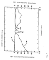
- FIG. 3 shows the frequency characteristics of the dual mode band-pass filter 1 of this embodiment.
- the reflection characteristic is represented by solid line A
- the transmission characteristic is done by broken line B (hereinafter, these characteristics will be represented in the same manner).
- a band-pass filter is formed in which the band indicated by arrow C is used as a transmission band.
- the two resonance modes are coupled to each other, due to the opening 3a formed in the metallic film 3, whereby characteristics suitable for the dual mode band-pass filter can be obtained.
- reference character W represents the length of a long side of the metallic film 3
- reference character L represents the length of a short side thereof.
- a first resonance mode is ⁇ /2 resonance mode (resonance frequency fr 1 ) of which the resonator length is the length in the long-side direction of the metallic film 3.
- a second resonance mode is a ⁇ /2 resonance mode (resonance frequency fr 2 ) of which the resonator length is the length in short-side direction of the metallic film 3.
- the measurements and the calculation values are substantially coincident with each other.
- the resonator formed by use of the rectangular metallic film 3 has two resonance modes, that is, one resonance mode is ⁇ /2 resonance in which the resonator length is the length W of a long side of the metallic film 3, and the other resonance mode is ⁇ /2 resonance in which the resonator length is the length of a short side of the metallic film 3.
- resonators Five types of resonators were prepared in which openings 3a with a width 1 of 0.2 mm and lengths W of 6, 8, 10, 12, and 13.5 mm were formed in a resonator containing the rectangular metallic film 3 with a size W ⁇ L of 15 ⁇ 7 mm prepared in the above experimental example.
- FIGS. 5 to 9 show the frequency characteristics of the five types of the resonators.
- the resonance current in the resonance mode propagated in the short-side direction is partially interrupted in the opening 3a, so that the resonance current acts as if an inductance were added, and therefore, the resonance frequency fr 2 in the resonance mode propagated in the short-side direction is reduced.
- the respective resonance currents flow differently from each other in the two resonance modes in the rectangular metallic film. Accordingly, for the purpose of coupling the two resonance modes as described above, the opening 3a is formed in such a manner that the resonance frequency in one of the resonance modes approaches the resonance frequency in the other resonance mode.
- the opening 3a is formed in such a manner that the two resonance modes can be coupled together. That is, when the resonator comprising the rectangular metallic film 3 is used, the lengthwise direction of the opening 3a is provided along the long side direction of the metallic film 3, and moreover, the size in the widthwise direction of the opening 3a is selected so that the resonance frequency in the resonance mode propagated in the short side direction of the metallic film 3 is reduced to approach the resonance frequency in the resonance mode propagated in the long side direction of the opening 3a.
- the filter can be operated as a dual mode band-pass filter, and moreover, the coupling degree can be controlled freely and significantly by adjusting the size of the opening 3a.
- FIG. 10A is a cross sectional view of a first modification example of the dual mode band-pass filter according to a first embodiment of the present invention.
- the metallic film 3 is formed on the upper face of the dielectric substrate 2.
- the metallic film 3 having the opening 3a is formed inside of the dielectric substrate 2.
- the plane shape of the metallic film 3 is similar to that of the first embodiment.
- ground electrodes 4 and 4 are formed on the whole of the upper and under faces of the dielectric substrate 1. Accordingly, the dual mode band-pass filter of this modification example has a tri-plate structure. Thus, the dual mode band-pass filter of the present invention may have the tri-plate structure.
- ground electrodes 4 may be formed in the form of internal electrodes at the middle in height of the dielectric substrate 2.
- FIG. 10B is a schematic plan view of a second modification example of the dual mode band-pass filter according to the first embodiment of the present invention.
- the input-output coupling circuits 5 and 6 are connected to one of the long sides of the rectangular metallic film 3. However, as shown in FIG. 10B, the input-output coupling circuits 5 and 6 are connected to the first and second long sides 3b and 3c, respectively.
- the other configuration is the same as that of the first embodiment.
- FIG. 11 shows the frequency characteristics of the dual mode band-pass filter of this modification example having the same configuration as the dual mode band-pass filter 1 of the first embodiment excepting that the connection points of the input-output coupling circuits 5 and 6 of this modification example are different from those of the first embodiment.
- characteristics suitable for a band-pass filter to be operated in a high frequency band can be obtained.
- the band-width can be considerably varied by changing the connection-point positions of the input-output coupling circuits 5 and 6. That is, the adjustment amount of the band-width and the design flexibility can be enhanced.
- FIG. 12 is a schematic plan view of a third modification example of the dual mode band-pass filter of the first embodiment.
- the metallic film 3 the length of a long side is set at 15 mm, and that of a short side is set at 13 mm.
- the band-pass filter of this modification example is configured similarly to that of the first embodiment.
- FIG. 13 shows the frequency characteristics of the dual mode band-pass filter of the second modification example. As seen in the comparison of FIG. 3 with FIG. 13, the bandwidth can be varied by changing the length of the short side of the metallic film 3.
- FIG. 14 is a perspective view of a dual mode band-pass filter according to a second embodiment of the present invention.
- FIG. 15 is a schematic plan view showing the main part of the dual mode band-pass filter.
- the dual mode band-pass filter 11 of the second embodiment is configured similarly in the same manner as that of the first embodiment excepting that the shape of a metallic film 13 formed on the upper face of the dielectric substrate 2 is different from that of the metallic film 3 of the first embodiment. Accordingly, similar parts are designated by the same reference numerals, and the repeated description is omitted.
- the shape of the metallic film constituting a resonator is not limited to a rectangle. That is, as shown in FIG. 14, the peripheral edge may have a random contour, that is, may have an optional contour. Also in this case, by forming an opening 13a in the metallic film 13 having an optional shape, and connecting the input-output coupling circuits 5 and 6 to two parts of the metallic film 13, a dual mode band-pass filter can be formed.
- the dielectric substrate 2 made of the same material and having the same thickness as that of the first embodiment.
- the metallic film 13 made of a copper film with a thickness of 18 ⁇ m and having an optional shape with a maximum diameter of 15 mm was prepared.
- a ground electrode was formed on the under face of the dielectric substrate 2 similarly to that of the first embodiment.
- connection points of the input-output coupling circuits 5 and 6 two optional points in the periphery of the metallic film 13 are selected as shown in FIGS. 14 and 15.
- the opening 13a is formed so as to be in parallel to the straight line passing through the two points.
- FIG. 16 shows the frequency characteristics of the dual mode band-pass filter of the second embodiment.
- the filter can be operated as a dual mode band-pass filter similarly to that of the first embodiment, by adjusting the length of the rectangular opening 13a.
- the shape of the metallic film 13 is optional, and moreover, the positional relations of the input-output coupling circuits 5 and 6 to the metallic film 13 are optional. That is, it is not necessary that the connection points of the input-output coupling circuits 5 and 6 are arranged so as to form an angle of 90° to each other with respect to the center of the metallic film 13.
- the opening 13a has a rectangular shape of which the length of a long side 11.5 mm and the length of a short side is 0.2 mm.
- the shape and size of the opening 13a are not limited to the above shape and values.
- the opening in the dual mode band-pass filter of the present invention is formed so as to couple two resonance modes. In this case, the resonance frequencies of the two resonance modes are different from each other, depending on the shape of the metallic film and the positions of the connection points of the input-output coupling circuits 5 and 6. Therefore, the shape and size of the opening 13a for coupling the two modes are changed correspondingly to the above-mentioned shape and the positions.
- the shape and size of the opening 13a in the second embodiment are varied, depending on the shape and size of the metallic film 14 and the positions of the connection points of the input-output coupling circuits 5 and 6. Therefore, the shape and size of the opening 13a can be concretely determined, correspondingly to the above-mentioned shape and positions.
- the opening 13a is formed so as to be in parallel to the imaginary straight line passing through the connection points of the input-output coupling circuits 5 and 6.
- the opening 13a interferes the resonance current caused by the resonance propagating in the perpendicular direction to the imaginary straight line passing through the above-mentioned connection points, whereby the two resonance modes are coupled.
- the two resonance modes can be securely coupled by adjusting the size in the lengthwise direction of the opening 13a, provided that two optional points in the periphery of the metallic film 13 are selected as the connection points, and the opening 13a is formed in parallel to the straight line passing through the two points.
- the opening 13a is formed so that the lengthwise direction of the opening 13a is in parallel to the imaginary straight line passing through the connection points of the input-output coupling circuits. Moreover, the length of the opening 13a is selected so that the two resonance modes, caused by the shape of the metallic film 13, can be coupled.
- FIG. 17 is a schematic plan view of a first modification example of the dual mode band-pass filter 11 of the second embodiment.
- the metallic film 13 and the opening 13a having the same shape and size of the second embodiment is formed.
- the connection points of the input-output coupling circuits 5. and 6 of this modification example are different from those of the second embodiment. That is, the connection points of the input-output coupling circuits 5 and 6 are arranged in the positions opposed to each other on the outer side of the part of the metallic film 13 where the opening 13a is formed, in the perpendicular direction to the lengthwise direction of the opening 13a.
- the other configuration is similar to that of the second embodiment.
- FIG. 18 shows the frequency characteristic of the dual mode band-pass filter of the above-described modification example.
- the bandwidth of the band-pass filter of the second embodiment is 1390 MHz
- the bandwidth of the band-pass filter of the first modification example is 490 MHz. That is, the bandwidths are equal to 20 % and 6.5 % of the center frequencies of the band-pass filters, respectively, are obtained.
- the bandwidth can be varied, and the coupling degree can be changed.
- FIG. 19 is a schematic plan view of a dual mode band-pass filter according to a third embodiment of the present invention.
- a metallic film 23 constituting a resonator takes a circular shape.
- a rectangular opening 23a is formed in the metallic film 23. It is not necessary that the connection points of the input-output coupling circuits 5 and 6 are provided in such positions as to form an center angle of 90° with respect to the circular metallic film 23.
- FIG. 20 shows the frequency characteristic of the band-pass filter of the third embodiment shown in FIG. 19.
- the characteristic shown in FIG. 20 is obtained when the circular metallic film 23 has a diameter of 15 mm, and a rectangular opening 23a with the length of a long side of 5 mm and the length of a short side of 0.2 mm is formed at a position shifted from the center of the metallic film 23.
- the other sizes are the same as those of the first embodiment.
- a dual mode band-pass filter can be also formed by using the circular metallic film 23a, and forming the opening 23a.
- the metallic film is circular
- the rectangular opening 23a is formed so that the lengthwise direction of a long side of the opening 23a is substantially in parallel to the imaginary line passing through the connection points of the input-output coupling circuits 5 and 6, the resonance current in the resonance mode propagated in the perpendicular direction to the imaginary line, not the resonance current in the resonance mode propagated substantially in parallel to the imaginary line, is affected by the opening 23a, though a circle has an isotropic shape, whereby the two resonance modes are coupled to form a dual mode band-pass filter.
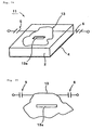
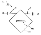
- FIG. 21 is a schematic plan view of a dual mode band-pass filter according to a fourth embodiment of the present invention.
- a metallic film 33 constituting a resonator has a square shape.
- a rectangular opening 33a is formed in the metallic film 33.
- the input-output coupling circuits 5 and 6 are connected to two points in the periphery of the metallic film 33. It is not necessary that the connection points of the input-output coupling circuits 5 and 6 are positioned so as to form a center angle of 90° with respect to the center of the square metallic film 33.
- FIG. 22 shows the frequency characteristics of the band-pass filter of the fourth embodiment shown in FIG. 21.
- the characteristics shown in FIG. 22 are obtained when the side length of the square metallic film 33 is 15 mm, and the opening 33a of with the length of a long side of 6 mm and that of a short side of 0.2 mm is formed in the square metallic film 33 at a position shifted from the center of the rectangular metallic film 33.
- the other sizes are the same as those of the first embodiment.
- a dual mode band-pass filter can be formed by use of the square metallic film 33, attributed to the formation of the opening 33a.
- FIG. 23 is a schematic plan view of a first modification example of the dual mode band-pass filter of the fourth embodiment.
- one opening 33a is formed.
- plural openings 33a and 33b may be formed, as shown in FIG. 23.
- FIG. 24 shows the frequency characteristic of a modification example of the band-pass filter shown in FIG. 23.
- the opening 33b has the same size as the opening 33a.
- the openings 33a and 33b are arranged in parallel to each other at an interval of 2 mm. The other sizes are the same as those of the fourth embodiment.
- FIG. 25 is a schematic plan view of a second modification example of the band-pass filter of the fourth embodiment.
- FIG. 26 shows the frequency characteristic.
- an opening 33c is formed in a metallic film 33.
- the opening 33c has bent parts 33c 1 and 33c 1 which are bent in the perpendicular direction to the lengthwise direction of the opening 33a (fourth embodiment) at both ends thereof.
- FIG. 26 shows the frequency characteristics obtained where the length of each bent part is set at 0.7 mm.
- the opening 33a is not limited to a rectangular shape and may take the shape in which the above-mentioned bent parts 33c 1 and 33c 1 are provided at both ends of a rectangle.
- FIG. 27 is a schematic plan view of a third modification example of the dual mode band-pass filter of the fourth embodiment.
- FIG. 28 shows the frequency characteristics thereof.
- a cross-shaped opening 33d is formed in the metallic film 33.
- the shape of the cross-shaped opening 33d corresponds to two rectangular openings crossed at a right angle, one rectangular opening thereof having a long-side length of 7 mm and a short-side length of 0.2 mm, the other rectangular opening having a long-side length of 4 mm and a short-side length of 0.2 mm.
- a dual mode band-pass filter can be also formed similarly to the fourth embodiment.
- plural openings may be provided, and not only a rectangular opening but also an opening having bend parts, and moreover, a cross-shaped opening may be employed. That is, the shape of the opening has no especial limitations.
- shapes such as rectangles and deformed rectangles, ellipses, circles, and so forth can be optionally used.
- shapes such as ellipses or the like, excluding rectangles, which have bent parts connected thereto as described above are available.
- a filter containing any of the above openings can be operated as a dual mode band-pass filter by adjusting the shape and size of the opening, similarly to the filter of each of the first to fourth embodiments.
- the opening has a symmetric shape in the resonance direction of at least one of the two resonance modes.
- FIG. 29 is a perspective view of a dual mode band-pass filter according to the fifth embodiment of the present invention.
- FIG. 30 is a schematic plan view showing the major part of the band-pass filter.
- FIG. 31 shows the frequency characteristics of the band-pass filter.
- a metallic film 43 constituting a resonator is formed so as to have a triangular shape.
- the dual mode band-pass filter 41 is similar to that of the first embodiment.
- a ground electrode 4 is formed on the same dielectric substrate 2 as that of the first embodiment.
- the equilaterally triangular metallic film 43 with the length of one side of 21 mm is formed.
- An opening 43a with the length of a long side of 10 mm and that of a short side of 0.2 mm is formed.
- the input-output coupling circuits 5 and 6 are connected to the different sides of the metallic film 43 at the positions thereof which are shifted from the opening 43a.
- the input-output coupling circuits 5 is not limited to the connection points shown in FIGS. 29 and 30. That is, it is not necessary that the input-output coupling circuits 5 and 6 are arranged so that the connection points form a center angle of 90° with respect to the center of the metallic film 43. Thus, the design flexibility can be enhanced.
- the filter can be also operated as a dual mode band-pass filter similarly to the band-pass filter of each of the first to fourth embodiments.
- the metallic film 43 has an equilateral triangle. It is not necessary that the shape of the metallic film 43 is an equilateral triangle.
- the metallic film 43 may be formed in an optional isosceles triangle.
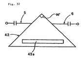
- FIG. 32 is a schematic plan view of a first modification example of the dual mode band-pass filter of the fifth example.
- FIG. 33 shows the frequency characteristics of the modification example.
- the dual mode band-pass filter of the first modification example is formed in the same manner as that of the fifth embodiment excepting that the plan shape of the metallic film 43 is the right isosceles triangle of which the vertical angle is 90°, and the length of the base is 21 mm.
- the band-pass filter can be operated as a dual mode band-pass filter by forming an opening 43a, and connecting the input-output coupling circuits 5 and 6 to two parts of the metallic film 43.
- FIG. 34 is a schematic plan view showing a second modification example of the dual mode band-pass filter of the fifth embodiment.
- FIG. 35 is a graph showing the frequency characteristics of the band-pass filter.
- the metallic film 43 having an isosceles triangular shape of which the vertical angle is 120° and the base length is 21 mm is formed.
- the band-pass filter is the same as that of the fifth embodiment.
- the filter can be also operated as a dual mode band-pass filter.
- two resonance modes can be coupled to form dual mode band-pass filters by forming the above-described openings in different types of isosceles triangles, adjusting the sizes of the openings, and connecting the input-output coupling circuits to different parts of the triangles, as seen in the fifth embodiment, and the first and second modification examples of the fifth embodiment.
- FIG. 36 is a perspective view showing the appearance of a dual mode band-pass filter 51 according to a sixth embodiment of the present invention.
- FIG. 37 is a schematic plan view of the band-pass filter.
- FIG. 38 is a graph showing the frequency characteristics of the band-pass filter.
- a metallic film 52 has a rhomboid shape.
- the band-pass filter 1 is the same as that of the first embodiment.
- a dielectric substrate and a ground electrode similar to those of the first embodiment were used, and a metal films 53 having a rhomboid shape with diagonal line lengths of 21 mm and 8 mm was formed.
- an opening 53a having a long-side length of 14 mm and a short-side length of 0.2 mm was formed in the metallic film 53.
- the input-output coupling circuits 5 and 6 were connected to the two different sides of the metallic film 53.
- the two resonance modes can be also coupled to each other, and a characteristic suitable for the dual mode band-pass filter can be obtained, attributed to the above-described configuration.
- the metallic film constituting a resonator may take a rhomboid shape as seen in the sixth embodiment.
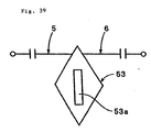
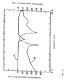
- FIG. 39 is a schematic plan view showing a first modification example of the dual mode band-pass filter of the sixth embodiment
- FIG. 40 is a graph showing the frequency characteristics thereof.
- the connection points of the input-output coupling circuits 5 and 6 are different from those in the sixth embodiment. That is, the input-output coupling circuits 5 and 6 are connected to a metallic film 53 so as to be opposed to each other, in the perpendicular direction to the long diagonal line of the metallic film.
- the pass-band filter is the same as that of the sixth embodiment.
- the two resonance modes can be coupled to each other. Furthermore, by comparing the frequency characteristics shown in FIGS. 39 and 40, it is seen that the bandwidth can be considerably varied by changing the connection points of the input-output coupling circuits 5 and 6.
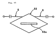
- FIG. 41 is a schematic plan view of a second modification example of the dual mode band-pass filter of the sixth embodiment
- FIG. 42 is a graph showing the frequency characteristic of the pass-band filter.
- the metallic film 53 has a rhomboid shape different from that in the sixth embodiment.
- the rhomboid shape of the metallic film 53 is different from that in the sixth embodiment. That is, the metallic film 53 is formed so as to have a rhomboid shape having diagonal line lengths of 21 mm and 12 mm.
- the band-pass filter is the same as that of the sixth embodiment.
- the bandwidth can be considerably varied by changing the rhomboid shape.
- FIG. 43 is a perspective view showing the appearance of a dual mode band-pass filter according to a seventh embodiment of the present invention
- FIG. 44 is a schematic plan view thereof.
- a metallic film 63 constituting a resonator takes a regular pentagonal shape.
- the configuration of the band-pass filter is the same as that in the first embodiment.
- FIG. 45 shows the frequency characteristics of the dual mode band-pass filter formed in the same manner as the experimental example of the first embodiment, excepting that a regular pentagon with a side-length of 9.5 mm is formed as the above-mentioned metallic film 63.
- the two resonance modes can be also coupled by adjusting the size of an opening 63a, whereby the band-pass filter can be operated as a dual mode band-pass filter.
- FIG. 46 is a schematic plan view showing the major part of a first modification example of the dual mode band-pass filter according to the seventh embodiment of the present invention, and FIG. 47 is the frequency characteristics thereof.
- the metallic film 63 takes a regular pentagonal shape.
- the shape of the metallic film is not limited to a regular pentagon.
- the metallic film may take a regular-hexagonal shape as presented in this modification example.
- the metallic film 63A was formed so that it took a regular hexagon with a side-length of 7.5 mm, and the other sizes of the band-pass filter were the same as those in the seventh embodiment. The frequency characteristic was measured.
- FIG. 47 shows the results.
- the two resonance modes can be coupled to each other, and the device can be operated as a dual mode band-pass filter, as seen in FIG. 47.
- the metallic film for constituting a resonator is formed on the dielectric substrate, and the size of the opening is adjusted, whereby the two resonance modes can be coupled to each other without the positions of the connection points of the input-output coupling circuits having no especial limitations, and a characteristic suitable for a dual mode band-pass filter can be obtained.
- the shape of the metallic film for constituting a resonator has a limitation, and the positions of the connection points of the input-output coupling circuits have a limitation.
- the dual mode band-pass filter of the present invention eliminates such limitations. Thus, the design flexibility can be considerably enhanced.
- the band-width can be significantly adjusted by changing the size of the metallic film, the size of the opening, and the positions of the connection points of the input-output coupling circuits.
- a dual mode band-pass filter having a desired band-width can be easily provided.
- the opening has such a plan shape as to contain a long-size direction and a short-size direction.
- the resonance current produced perpendicularly to the long-size direction is interrupted by the opening.
- the resonance frequency of the resonance propagated perpendicularly to the long-size direction of the opening can be easily changed. Thereby, the two resonance modes can be securely coupled to each other.
- the opening and the plan shape of the metallic film have no especial limitations, respectively.
- Dual mode band-pass filters having different shapes of openings and metallic films can be provided.
- a rectangle, an ellipse, a shape comprising a rectangle or ellipse having a bent part thereof elongating in a direction intersecting the long-size direction, or a cross shape can be optionally employed.
- plural openings may be formed.
- the band-width can be adjusted by changing the number of the openings.
- the metallic film and the ground electrode may be formed either on the surface of the dielectric substrate or inside thereof.
- the dual mode band-pass filter of the present invention can be simply formed by forming conductive films on both surfaces of a dielectric substrate, respectively.
Description
- The present invention relates to a dual mode band-pass filter for use in, e.g., a communication equipment operating in the range of the microwave band to the milliwave band.
- Conventionally, different types of dual mode band-pass filters have been proposed as a band-pass filter for use in a high frequency band as described in MINIATURE DUAL MODE MICROSTRIP FILTERS, J. A. Curtis and S.J. Fiedziuszko, 1991 IEE MTT-S Digest, and so forth.
- FIGS. 48 and 49 are schematic plan views illustrating conventional dual mode band-pass filters, respectively.
- In a band-
pass filter 200 shown in FIG. 48, a circularconductive film 201 is formed on a dielectric substrate (not shown). Input-output coupling circuits conductive film 201 so as to form an angle of 90° to each other. A tip-open stub 204 is formed on theconductive film 201 at the position thereof forming a central angle of 45° to the input-output coupling circuit 203. Thereby, two resonance modes with different resonance frequencies are coupled. Thus, the band-pass filter 200 is configured so as to operate as a dual mode band-pass filter. - In a dual mode band-
pass filter 210 shown in FIG. 49, a substantially squareconductive film 211 is formed on a dielectric substrate. Input-output coupling circuits conductive film 211 so as to form an angle of 90° to each other. The corner of theconductive film 211 in the position thereof forming an angle of 135° with respect to the input-output coupling circuit 213 is cut away. The resonance frequencies in two resonance modes are made different from each other by the formed thecut portion 211a, so that the two resonance modes are coupled to each other. Thus, the band-pass filter 210 can be operated as a dual mode band-pass filter. - On the other hand, there has been proposed a dual mode band-pass filter which contains a ring-shape conductive film instead of the circular conductive film (Japanese Unexamined Patent Application Publication No. 9-139612 and No. 9-162610, and so forth). In particular, a dual mode filter is disclosed, in which a ring-shaped ring transmission line is used, input-output coupling circuits are arranged so as to form a central angle of 90° similarly to the dual mode band-
pass filter 200 shown in FIG. 48, and a tip-open stub is provided in a part of the ring transmission line. - Moreover, Japanese Unexamined Patent Application Publication No. 6-112701 discloses a dual mode band-pass filter which uses a ring transmission line similar to the above-mentioned transmission line. As shown in FIG. 50, in the
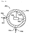
dual mode filter 221, a ring resonator is formed in which a ringconductive film 222 is formed on a dielectric substrate. In this case, fourterminals 223 to 226 are formed on the ringconductive film 222 so as to form an angle of 90° to each other with respect to the center of the ringconductive film 222. Two of the four terminals arranged at the positions forming an angle of 90° to each other with respect to the center of the ring conductive film are connected to input-output coupling circuits terminals feedback circuit 230. - Moreover, it is described that in the ring resonator comprising one strip line and having the above-described configuration, orthogonal resonance modes, not coupled to each other, are generated, and the coupling degree is controlled by means of the above-mentioned
feedback circuit 230. - In the conventional dual mode band-pass filters shown in FIGS. 48 and 49, a two step band-pass filter can be formed by forming one conductive film pattern. Accordingly, the band-pass filter can be miniaturized.
- However, the dual mode band-pass filters each have the configuration in which the input-output coupling circuits, separated from each other by an particular angle, are coupled to each other in the circular or square conductive film pattern. Therefore, the dual mode band-pass filters have the disadvantage that the coupling degree cannot be increased, and a wide pass band can not be attained.
- In the band-pass filter shown in FIG. 48, the
conductive film 201 is restricted substantially onto a circular shape. In the band-pass filter shown in FIG. 49, theconductive film 211 is also limited to a substantially square shape. There is the problem that the design flexibility is low. - Dual mode band-
pass filters 221 using such a ring resonator as described in Japanese Unexamined Patent Application Publication Nos. 9-139612 and 9-162610 have the problem that it is difficult to enhance the coupling degree, and the shape and size of the ring resonator are restricted. - On the other hand, in the dual mode band-
pass filter 221 described in Japanese Unexamined Patent Application Publication No. 6-112701, the coupling degree is controlled, and the band-width can be widened by use of thefeedback circuit 230. However, in the dual mode filter described as the conventional technique, thefeedback circuit 230 is required. Thus, there is caused the problem that the circuit configuration becomes complicated. Furthermore, problematically, the shape and size of the ring resonator is limited to a ring-shape, so that the design flexibility becomes low. -
EP 0 571 777 A1 describes a strip dual mode loop resonator having a loop-shaped strip line with a pair of straight strip lines arranged in parallel. Microwaves transferred from an input strip line to the loop-shaped strip line results in a reflection of the microwave in the straight strip lines of the loop-shaped strip line to produce reflected microwaves circulated in opposite directions. Thereafter, the reflected waves are resonated and filtered in dual mode in the loop-shaped strip line and provided to an outer strip line. - EP-A-0 509 636 discloses a dual mode microstrip resonator usable in the design of microwave communication filters. The substantially square resonator provides paths for a pair of orthogonal signals which are coupled together using a perturbation located in at least one corner of the resonator.
- It is the object of the present invention to provide a method for designing a dual mode band-pass filter providing for a miniaturization of the device, an enhancement of the coupling degree, an easy adjustment of the coupling degree providing for the realization of a wide pass band and providing for a high design flexibility.
- This object is achieved by a method according to claim 1.
- The present invention provides a dual mode band-pass filter which comprises a dielectric substrate having first and second main faces, a metallic film having an opening for coupling two resonance modes and formed in the first main face of the dielectric substrate or inside of the dielectric substrate, at least one ground electrode formed on the second main face of the dielectric substrate or inside of the dielectric substrate, so as to be opposed to the metallic film through a dielectric layer, and a pair of input-output coupling circuits connected to different parts of the metallic film. With the above-described configuration, one of the two resonance modes, that is, one propagated in parallel to the imaginary straight line passing through the connection points at which a pair of the input-output coupling circuits are connected to the metallic film, and the other propagated perpendicularly to the imaginary line, is affected by the opening so that the resonance frequency is varied. In other words, the opening is formed so as to exert an influence over the resonance current of one of the resonance modes whereby the one resonance mode can be coupled to the other resonance mode. Thus, the opening causes the two resonance modes to be coupled to each other, and the filter can be operated as a dual mode band-pass filter.
- Preferably, the opening has a shape containing a long-size direction and a short-size direction.
- Also preferably, the plan shape of the opening is a rectangle, an ellipse, or a shape comprising a rectangle or ellipse having a bent part thereof elongating in a direction intersecting the long-size direction.
- Yet preferably, the plan shape of the opening is a rectangle, a rhombus, a regular polygon, a circle, or an ellipse.
- Plural openings may be formed.
- Preferably, the metallic film is formed on the first main face of the dielectric substrate, and the ground electrode is formed on the second main face.
- Also preferably, the metallic film is formed on a height level inside of the dielectric substrate, and the ground electrodes are formed on the first and second main faces of the dielectric substrate, whereby the band-pass filter has a tri-plate structure.
-
- FIG. 1 is a perspective view of a dual mode band-pass filter according to a first embodiment of the present invention;
- FIG. 2 is a schematic plan view showing the major part of the dual mode band-pass filter of the first embodiment;
- FIG. 3 is a graph showing the frequency characteristics of the dual mode band-pass filter of the first embodiment;
- FIG. 4 is a graph showing the frequency characteristics of a resonator produced by forming a rectangular metallic film having no opening on a dielectric substrate;
- FIG. 5 is a graph showing the frequency characteristics of a dual mode band-pass filter formed in a concrete experimental example of the first embodiment, in which the size of the metallic film is 15 x 7 mm, the length of an opening is 6 mm, and the width of the opening is 0.2 mm;
- FIG. 6 is a graph showing the frequency characteristics of the dual mode band-pass filter formed in the concrete experimental example of the first embodiment, in which the size of the metallic film is 15 x 7 mm, the length of the opening is 8 mm, and the width of the opening is 0.2 mm;
- FIG. 7 is a graph showing the frequency characteristics of the dual mode band-pass filter formed in the concrete experimental example of the first embodiment, in which the size of the metallic film is 15 x 7 mm, the length of the opening is 10 mm, and the width of the opening is 0.2 mm;
- FIG. 8 is a graph showing the frequency characteristics of the dual mode band-pass filter formed in the concrete experimental example of the first embodiment, in which the size of the metallic film is 15 x 7 mm, the length of the opening is 12 mm, and the width of the opening is 0.2 mm;
- FIG. 9 is a graph showing the frequency characteristics of the dual mode band-pass filter formed in a concrete experimental example of the first embodiment, in which the size of the metallic film is 15 x 7 mm, the length of the opening is 13.5 mm, and the width of the opening is 0.2 mm;
- FIG. 10A is a cross sectional view of a dual mode band-pass filter according to a first modification example of the first embodiment;
- FIG. 10B is a schematic plan view showing the main part of a dual mode band-pass filter according to a second modification example of the first embodiment;
- FIG. 11 is a graph showing the frequency characteristics of the dual mode band-pass filter of the second example of the first embodiment;
- FIG. 12 is a schematic plan view of a dual mode band-pass filter according to a third modification example of the first embodiment;
- FIG. 13 is a graph showing the frequency characteristic of the dual mode band-pass filter of the third modification example of the first embodiment;
- FIG. 14 is a perspective view showing the appearance of a dual mode band-pass filter according to a second embodiment of the present invention;
- FIG. 15 is a schematic plan view showing the main part of the dual mode band-pass filter of the second embodiment;
- FIG. 16 is a graph showing the frequency characteristics of the dual mode band-pass filter of the second embodiment;
- FIG. 17 is a schematic plan view of a dual mode band-pass filter according to a first modification example of the second example;
- FIG. 18 is a graph showing the frequency characteristics of the dual mode band-pass filter of the first modification example of the second embodiment;
- FIG. 19 is a schematic plan view of a dual mode band-pass filter according to a third embodiment of the present invention;
- FIG. 20 is a graph showing the frequency characteristics of the dual mode band-pass filter of the third embodiment;
- FIG. 21 is a schematic plan view of a dual mode band-pass filter according to a fourth embodiment of the present invention;
- FIG. 22 is the frequency characteristics of the dual mode band-pass filter of the fourth embodiment;
- FIG. 23 is a schematic plan view of a dual mode band-pass filter according to a first modification example of the fourth embodiment;
- FIG. 24 is a graph showing the frequency characteristics of the dual mode band-pass filter of the first modification example of the fourth embodiment;
- FIG. 25 is a schematic plan view of a dual mode band-pass filter according to a second modification example of the fourth embodiment;
- FIG. 26 is a graph showing the frequency characteristics of the dual mode band-pass filter of the second modification example of the fourth embodiment;
- FIG. 27 is a schematic plan view of a dual mode band-pass filter according to a third modification example of the fourth embodiment;
- FIG. 28 is the frequency characteristics of the dual mode band-pass filter of the third modification example of the fourth embodiment;
- FIG. 29 is a perspective view of a dual mode band-pass filter according to a fifth embodiment of the present invention;
- FIG. 30 is a schematic plan view showing the main part of the dual of the fifth embodiment;
- FIG. 31 is a graph showing the frequency characteristics of the dual mode band-pass filter of the fifth embodiment;
- FIG. 32 is a schematic plan view showing a dual mode band-pass filter according to a first modification example of the fifth embodiment;
- FIG. 33 is a graph showing the frequency characteristics of the dual mode band-pass filter of the first modification example of the fifth embodiment;
- FIG. 34 is a schematic plan view of a dual mode band-pass filter according to a second modification example of the fifth embodiment;
- FIG. 35 is a graph showing the frequency characteristics of the dual mode band-pass filter of the second modification example of the fifth embodiment;
- FIG. 36 is a perspective view of a dual mode band-pass filter according to a sixth embodiment of the present invention;
- FIG. 37 is a schematic plan view showing the main part of the dual mode band-pass filter of the sixth embodiment;
- FIG. 38 is a graph showing the frequency characteristics of the dual mode band-pass filter of the sixth embodiment;
- FIG. 39 is a schematic plan view of a dual mode band-pass filter according to a first modification example of the sixth embodiment;
- FIG. 40 is a graph showing the frequency characteristics of the dual mode band-pass filter of the first modification example of the sixth embodiment;
- FIG. 41 is a schematic plan view of a dual mode band-pass filter according to a second modification example of the sixth embodiment;
- FIG. 42 is a graph showing the frequency characteristics of the dual mode band-pass filter of the second modification example of the sixth embodiment;
- FIG. 43 is a perspective view of a dual mode band-pass filter according to a seventh embodiment of the present invention;
- FIG. 44 is a schematic plan view showing the main part of the dual mode band-pass filter of the seventh embodiment;
- FIG. 45 is the frequency characteristics of the dual mode band-pass filter of the seventh embodiment;
- FIG. 46 is a schematic plan view of a dual mode band-pass filter according to a first modification example of the seventh embodiment;
- FIG. 47 is a graph showing the frequency characteristics of the dual mode band-pass filter of the first modification example of the seventh embodiment;
- FIG. 48 is a schematic plan view showing an example of a conventional dual mode band-pass filter;
- FIG. 49 is a schematic plan view showing another example of the conventional dual mode band-pass filter; and
- FIG. 50 is a schematic plan view showing yet another example of the conventional dual mode band-pass filter.
- Hereinafter, concrete embodiments of the present invention will be described to make more apparent the present invention.
- FIG. 1 is a perspective view of a dual mode band-pass filter according to a first embodiment of the present invention. FIG. 2 is a schematic plan view of the dual mode band-pass filter;
- A dual mode band-pass filter 1 contains a rectangular sheet
dielectric substrate 2. In this embodiment, thedielectric substrate 2 is made of a fluororesin having a dielectric constant εr of 2.58. However, in this and below-described embodiments, as dielectric materials for forming the dielectric substrate, appropriate dielectric materials such as BaO-Al2O3-SiO2 type ceramics or the like can be used, in addition to the fluororesin. - The thickness of the above-described
dielectric substrate 2 has no particular limitations. In this embodiment, the thickness is set at 350 µm. - A
metallic film 3 is formed on the upper face 2a of thedielectric substrate 2 to produce a resonator. Themetallic film 3 is formed in a partial area on thedielectric substrate 2, and takes a rectangular shape with long and short sides in this embodiment. Anopening 3a is formed in themetallic film 3. Theopening 3a has a rectangular plane shape similar to that of themetallic film 3a. The lengthwise direction (long-side direction) of theopening 3a is parallel to the longitudinal direction, namely, the long-side direction, of themetallic film 3. - In this embodiment, the length W of each long side of the
metallic film 3 is 15 mm, and the length L of each short side is 7 mm. For theopening 3a, the length w of each long side is 13.5 mm, and the length 1 of each short side is 0.2 mm. However, the sizes of themetallic film 3 and theopening 3a are not limited to the above values. The shapes of themetallic film 3 and theopening 3a can be modified, correspondingly to desired center frequency and bandwidth. - On the other hand, a
ground electrode 4 is formed on the whole of the under face of thedielectric substrate 2. - Input-
output coupling circuits long sides 3b of themetallic film 3, respectively. The input-output coupling circuits metallic film 3, provided that the positions are different from each other on themetallic film 3. - In the dual mode band-pass filter of this embodiment, an input voltage is applied between one of the input-
output coupling circuits ground electrode 4, whereby a predetermined output power between the other circuit of the input-output coupling circuits ground electrode 4 is output. In this case, the two resonance modes are coupled to each other, since themetallic film 3 has a rectangular shape, and theopening 3a is formed. Thus, this filter operates as a dual mode band-pass filter. FIG. 3 shows the frequency characteristics of the dual mode band-pass filter 1 of this embodiment. - In FIG. 3, the reflection characteristic is represented by solid line A, and the transmission characteristic is done by broken line B (hereinafter, these characteristics will be represented in the same manner). As seen in FIG. 3, a band-pass filter is formed in which the band indicated by arrow C is used as a transmission band.
- In particular, it is seen that in the dual mode band-pass filter of this embodiment, the two resonance modes are coupled to each other, due to the
opening 3a formed in themetallic film 3, whereby characteristics suitable for the dual mode band-pass filter can be obtained. - By changing the shape of the
metallic film 3 in the above-described configuration, various resonance characteristics of the two modes can be obtained. This will be described in reference to a concrete experimental example. -
Metallic films 3 made of copper, having a rectangular plane shape, and eliminating theopening 3a, which had different sizes as listed in TABLE 1, were formed on the dielectric substrate. Thereby, four types of resonators were prepared. In TABLE 1, reference character W represents the length of a long side of themetallic film 3, and reference character L represents the length of a short side thereof. - As resonance modes based on the resonators comprising these metallic films, the following two modes are probable. A first resonance mode is λ/2 resonance mode (resonance frequency fr1) of which the resonator length is the length in the long-side direction of the
metallic film 3. A second resonance mode is a λ/2 resonance mode (resonance frequency fr2) of which the resonator length is the length in short-side direction of themetallic film 3. - The measurements and calculation values of the resonance frequencies fr1 and fr2 are listed in the following TABLE 1.
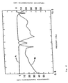
- The frequency characteristic of the
metallic film 3 with W × L = 15 × 13 mm, eliminating the opening, is illustrated as a typical example in FIG. 4.[TABLE 1] W × L (mm) measurements calculation values fr1(GHz) fr2(GHz) fr1(GHz) fr2(GHz) 15 × 13 6.29 7.13 6.22 7.18 15 × 11 6.22 8.63 6.22 8.48 15 × 9 6.16 10.51 6.22 10.37 15 × 7 6.22 13.24 6.22 13.33 - As seen in TABLE 1, the measurements and the calculation values are substantially coincident with each other. In the above-described results, it is seen that the resonator formed by use of the rectangular
metallic film 3 has two resonance modes, that is, one resonance mode is λ/2 resonance in which the resonator length is the length W of a long side of themetallic film 3, and the other resonance mode is λ/2 resonance in which the resonator length is the length of a short side of themetallic film 3. - Hereinafter, it will be described that by forming the
opening 3a in the rectangularmetallic film 3, the above-mentioned two resonance modes can be coupled, whereby a dual mode band-pass filter can be obtained. - Five types of resonators were prepared in which
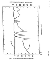
openings 3a with a width 1 of 0.2 mm and lengths W of 6, 8, 10, 12, and 13.5 mm were formed in a resonator containing the rectangularmetallic film 3 with a size W × L of 15 × 7 mm prepared in the above experimental example. - FIGS. 5 to 9 show the frequency characteristics of the five types of the resonators.
- As seen in FIGS. 5 to 9, the larger the length W of the
opening 3a becomes, the more the resonance frequency fr2 of the second resonance mode shifts to the low frequency side. Furthermore, as seen in FIG. 9, when the resonance frequency fr2 becomes lower than the resonance frequency fr1, the resonance frequencies fr1 and fr2 couple together, whereby a band-pass filter is formed. - Presumably, in the dual mode band-pass filter of this embodiment, the resonance current in the resonance mode propagated in the short-side direction is partially interrupted in the
opening 3a, so that the resonance current acts as if an inductance were added, and therefore, the resonance frequency fr2 in the resonance mode propagated in the short-side direction is reduced. In other words, in the dual mode band-pass filter of this embodiment, the respective resonance currents flow differently from each other in the two resonance modes in the rectangular metallic film. Accordingly, for the purpose of coupling the two resonance modes as described above, theopening 3a is formed in such a manner that the resonance frequency in one of the resonance modes approaches the resonance frequency in the other resonance mode. - As described above, the
opening 3a is formed in such a manner that the two resonance modes can be coupled together. That is, when the resonator comprising the rectangularmetallic film 3 is used, the lengthwise direction of theopening 3a is provided along the long side direction of themetallic film 3, and moreover, the size in the widthwise direction of theopening 3a is selected so that the resonance frequency in the resonance mode propagated in the short side direction of themetallic film 3 is reduced to approach the resonance frequency in the resonance mode propagated in the long side direction of theopening 3a. - Accordingly, as described above, the filter can be operated as a dual mode band-pass filter, and moreover, the coupling degree can be controlled freely and significantly by adjusting the size of the
opening 3a. - FIG. 10A is a cross sectional view of a first modification example of the dual mode band-pass filter according to a first embodiment of the present invention.
- In the first embodiment, the
metallic film 3 is formed on the upper face of thedielectric substrate 2. In the dual mode band-pass filter of the first modification example shown in FIG. 10A, themetallic film 3 having theopening 3a is formed inside of thedielectric substrate 2. The plane shape of themetallic film 3 is similar to that of the first embodiment. - Furthermore,
ground electrodes - It is not necessary to form the
ground electrodes 4 on the whole of the faces of thedielectric substrate 2, provided that theground electrodes 4 are opposed to each other through themetallic film 3 and thedielectric substrate 2 or through a part of the layers of thedielectric substrate 2. In addition, theground electrodes 4 may be formed in the form of internal electrodes at the middle in height of thedielectric substrate 2. - FIG. 10B is a schematic plan view of a second modification example of the dual mode band-pass filter according to the first embodiment of the present invention.
- In the dual mode band-pass filter 1 of the first embodiment, the input-
output coupling circuits metallic film 3. However, as shown in FIG. 10B, the input-output coupling circuits long sides - FIG. 11 shows the frequency characteristics of the dual mode band-pass filter of this modification example having the same configuration as the dual mode band-pass filter 1 of the first embodiment excepting that the connection points of the input-
output coupling circuits output coupling circuits - FIG. 12 is a schematic plan view of a third modification example of the dual mode band-pass filter of the first embodiment. In this modification example, regarding the
metallic film 3, the length of a long side is set at 15 mm, and that of a short side is set at 13 mm. In other respects, the band-pass filter of this modification example is configured similarly to that of the first embodiment. - FIG. 13 shows the frequency characteristics of the dual mode band-pass filter of the second modification example. As seen in the comparison of FIG. 3 with FIG. 13, the bandwidth can be varied by changing the length of the short side of the
metallic film 3. - FIG. 14 is a perspective view of a dual mode band-pass filter according to a second embodiment of the present invention. FIG. 15 is a schematic plan view showing the main part of the dual mode band-pass filter.
- The dual mode band-
pass filter 11 of the second embodiment is configured similarly in the same manner as that of the first embodiment excepting that the shape of ametallic film 13 formed on the upper face of thedielectric substrate 2 is different from that of themetallic film 3 of the first embodiment. Accordingly, similar parts are designated by the same reference numerals, and the repeated description is omitted. - In the dual mode band-pass filter of the present invention, the shape of the metallic film constituting a resonator is not limited to a rectangle. That is, as shown in FIG. 14, the peripheral edge may have a random contour, that is, may have an optional contour. Also in this case, by forming an
opening 13a in themetallic film 13 having an optional shape, and connecting the input-output coupling circuits metallic film 13, a dual mode band-pass filter can be formed. - A concrete experimental example and the frequency characteristic of the dual mode band-
pass filter 11 will be described. Thedielectric substrate 2 made of the same material and having the same thickness as that of the first embodiment. Moreover, themetallic film 13 made of a copper film with a thickness of 18 µm and having an optional shape with a maximum diameter of 15 mm was prepared. A ground electrode was formed on the under face of thedielectric substrate 2 similarly to that of the first embodiment. - Referring to the connection points of the input-
output coupling circuits metallic film 13 are selected as shown in FIGS. 14 and 15. Theopening 13a is formed so as to be in parallel to the straight line passing through the two points. - FIG. 16 shows the frequency characteristics of the dual mode band-pass filter of the second embodiment.
- As seen in FIG. 16, two resonance modes are coupled to each other, whereby a frequency characteristic suitable for a dual mode band-pass filter can be obtained. That is, even if the shape of the
metallic film 13 is optional, the filter can be operated as a dual mode band-pass filter similarly to that of the first embodiment, by adjusting the length of therectangular opening 13a. - In the second embodiment, the shape of the
metallic film 13 is optional, and moreover, the positional relations of the input-output coupling circuits metallic film 13 are optional. That is, it is not necessary that the connection points of the input-output coupling circuits metallic film 13. - In the dual mode band-
pass filter 11 of the second embodiment, theopening 13a has a rectangular shape of which the length of a long side 11.5 mm and the length of a short side is 0.2 mm. The shape and size of theopening 13a are not limited to the above shape and values. As seen in the description of the first example, the opening in the dual mode band-pass filter of the present invention is formed so as to couple two resonance modes. In this case, the resonance frequencies of the two resonance modes are different from each other, depending on the shape of the metallic film and the positions of the connection points of the input-output coupling circuits opening 13a for coupling the two modes are changed correspondingly to the above-mentioned shape and the positions. - That is, the shape and size of the
opening 13a in the second embodiment are varied, depending on the shape and size of the metallic film 14 and the positions of the connection points of the input-output coupling circuits opening 13a can be concretely determined, correspondingly to the above-mentioned shape and positions. - However, as seen in the description of the first embodiment, the
opening 13a is formed so as to be in parallel to the imaginary straight line passing through the connection points of the input-output coupling circuits opening 13a interferes the resonance current caused by the resonance propagating in the perpendicular direction to the imaginary straight line passing through the above-mentioned connection points, whereby the two resonance modes are coupled. Accordingly, as seen in the experimental example of the first embodiment, the two resonance modes can be securely coupled by adjusting the size in the lengthwise direction of theopening 13a, provided that two optional points in the periphery of themetallic film 13 are selected as the connection points, and theopening 13a is formed in parallel to the straight line passing through the two points. In other words, theopening 13a is formed so that the lengthwise direction of theopening 13a is in parallel to the imaginary straight line passing through the connection points of the input-output coupling circuits. Moreover, the length of theopening 13a is selected so that the two resonance modes, caused by the shape of themetallic film 13, can be coupled. - FIG. 17 is a schematic plan view of a first modification example of the dual mode band-
pass filter 11 of the second embodiment. In this modification example, themetallic film 13 and theopening 13a having the same shape and size of the second embodiment is formed. However, the connection points of the input-output coupling circuits 5. and 6 of this modification example are different from those of the second embodiment. That is, the connection points of the input-output coupling circuits metallic film 13 where theopening 13a is formed, in the perpendicular direction to the lengthwise direction of theopening 13a. The other configuration is similar to that of the second embodiment. - FIG. 18 shows the frequency characteristic of the dual mode band-pass filter of the above-described modification example.
- By comparing FIG. 16 with FIG. 18, it is seen that the bandwidth of the band-pass filter of the second embodiment is 1390 MHz, and the bandwidth of the band-pass filter of the first modification example is 490 MHz. That is, the bandwidths are equal to 20 % and 6.5 % of the center frequencies of the band-pass filters, respectively, are obtained. Thus, it is seen that by changing the positions of the connection points of the input-
output coupling circuits - FIG. 19 is a schematic plan view of a dual mode band-pass filter according to a third embodiment of the present invention. In a dual mode band-
pass filter 21 of the third embodiment, ametallic film 23 constituting a resonator takes a circular shape. A rectangular opening 23a is formed in themetallic film 23. It is not necessary that the connection points of the input-output coupling circuits metallic film 23. - FIG. 20 shows the frequency characteristic of the band-pass filter of the third embodiment shown in FIG. 19. The characteristic shown in FIG. 20 is obtained when the circular
metallic film 23 has a diameter of 15 mm, and a rectangular opening 23a with the length of a long side of 5 mm and the length of a short side of 0.2 mm is formed at a position shifted from the center of themetallic film 23. The other sizes are the same as those of the first embodiment. - As seen in FIG. 20, in the third embodiment, a dual mode band-pass filter can be also formed by using the circular metallic film 23a, and forming the opening 23a. In particular, in the case of the metallic film is circular, and the rectangular opening 23a is formed so that the lengthwise direction of a long side of the opening 23a is substantially in parallel to the imaginary line passing through the connection points of the input-
output coupling circuits - FIG. 21 is a schematic plan view of a dual mode band-pass filter according to a fourth embodiment of the present invention. In the dual mode band-pass filter of the fourth embodiment, a
metallic film 33 constituting a resonator has a square shape. Arectangular opening 33a is formed in themetallic film 33. The input-output coupling circuits metallic film 33. It is not necessary that the connection points of the input-output coupling circuits metallic film 33. - FIG. 22 shows the frequency characteristics of the band-pass filter of the fourth embodiment shown in FIG. 21. The characteristics shown in FIG. 22 are obtained when the side length of the square
metallic film 33 is 15 mm, and theopening 33a of with the length of a long side of 6 mm and that of a short side of 0.2 mm is formed in the squaremetallic film 33 at a position shifted from the center of the rectangularmetallic film 33. The other sizes are the same as those of the first embodiment. - As seen in FIG. 22, also in the third embodiment, a dual mode band-pass filter can be formed by use of the square
metallic film 33, attributed to the formation of theopening 33a. - FIG. 23 is a schematic plan view of a first modification example of the dual mode band-pass filter of the fourth embodiment. In the fourth embodiment, one
opening 33a is formed. However,plural openings opening 33b has the same size as theopening 33a. Theopenings - FIG. 25 is a schematic plan view of a second modification example of the band-pass filter of the fourth embodiment. FIG. 26 shows the frequency characteristic. In the dual mode band-pass filter of the second modification example, an
opening 33c is formed in ametallic film 33. Theopening 33c has bentparts opening 33a (fourth embodiment) at both ends thereof. FIG. 26 shows the frequency characteristics obtained where the length of each bent part is set at 0.7 mm. - As seen in FIGS. 25 and 26, the
opening 33a is not limited to a rectangular shape and may take the shape in which the above-mentionedbent parts - FIG. 27 is a schematic plan view of a third modification example of the dual mode band-pass filter of the fourth embodiment. FIG. 28 shows the frequency characteristics thereof. In the dual mode band-pass filter of the third modification example, a
cross-shaped opening 33d is formed in themetallic film 33. The shape of thecross-shaped opening 33d corresponds to two rectangular openings crossed at a right angle, one rectangular opening thereof having a long-side length of 7 mm and a short-side length of 0.2 mm, the other rectangular opening having a long-side length of 4 mm and a short-side length of 0.2 mm. As seen in FIGS. 27 and 28, in the case in which thecross-shaped opening 33d is formed, a dual mode band-pass filter can be also formed similarly to the fourth embodiment. - As seen in the first to the third modification examples of the fourth embodiment, in the dual mode band-pass filter of the present invention, plural openings may be provided, and not only a rectangular opening but also an opening having bend parts, and moreover, a cross-shaped opening may be employed. That is, the shape of the opening has no especial limitations. In addition to the above-mentioned different types of shapes such as rectangles and deformed rectangles, ellipses, circles, and so forth can be optionally used. Furthermore, shapes such as ellipses or the like, excluding rectangles, which have bent parts connected thereto as described above are available. A filter containing any of the above openings can be operated as a dual mode band-pass filter by adjusting the shape and size of the opening, similarly to the filter of each of the first to fourth embodiments. Desirably, the opening has a symmetric shape in the resonance direction of at least one of the two resonance modes.
- FIG. 29 is a perspective view of a dual mode band-pass filter according to the fifth embodiment of the present invention. FIG. 30 is a schematic plan view showing the major part of the band-pass filter. FIG. 31 shows the frequency characteristics of the band-pass filter.
- In the dual mode band-
pass filter 41 of the fifth embodiment, ametallic film 43 constituting a resonator is formed so as to have a triangular shape. In the other respects, the dual mode band-pass filter 41 is similar to that of the first embodiment. - A
ground electrode 4 is formed on the samedielectric substrate 2 as that of the first embodiment. The equilaterally triangularmetallic film 43 with the length of one side of 21 mm is formed. Anopening 43a with the length of a long side of 10 mm and that of a short side of 0.2 mm is formed. The input-output coupling circuits metallic film 43 at the positions thereof which are shifted from theopening 43a. The input-output coupling circuits 5 is not limited to the connection points shown in FIGS. 29 and 30. That is, it is not necessary that the input-output coupling circuits metallic film 43. Thus, the design flexibility can be enhanced. - As shown in FIG. 31, in the case of the
metallic film 43 having the equilaterally triangular shape, the filter can be also operated as a dual mode band-pass filter similarly to the band-pass filter of each of the first to fourth embodiments. - In the fifth embodiment, the
metallic film 43 has an equilateral triangle. It is not necessary that the shape of themetallic film 43 is an equilateral triangle. Themetallic film 43 may be formed in an optional isosceles triangle. - FIG. 32 is a schematic plan view of a first modification example of the dual mode band-pass filter of the fifth example. FIG. 33 shows the frequency characteristics of the modification example. The dual mode band-pass filter of the first modification example is formed in the same manner as that of the fifth embodiment excepting that the plan shape of the
metallic film 43 is the right isosceles triangle of which the vertical angle is 90°, and the length of the base is 21 mm. As seen in FIGS. 32 and 33, in the use of themetallic film 43 having the right triangle, the band-pass filter can be operated as a dual mode band-pass filter by forming anopening 43a, and connecting the input-output coupling circuits metallic film 43. - FIG. 34 is a schematic plan view showing a second modification example of the dual mode band-pass filter of the fifth embodiment. FIG. 35 is a graph showing the frequency characteristics of the band-pass filter.
- In the second modification example, the
metallic film 43 having an isosceles triangular shape of which the vertical angle is 120° and the base length is 21 mm is formed. In the other respects, the band-pass filter is the same as that of the fifth embodiment. As seen in FIGS. 34 and 35, in the second modification example, the filter can be also operated as a dual mode band-pass filter. - According to the present invention, two resonance modes can be coupled to form dual mode band-pass filters by forming the above-described openings in different types of isosceles triangles, adjusting the sizes of the openings, and connecting the input-output coupling circuits to different parts of the triangles, as seen in the fifth embodiment, and the first and second modification examples of the fifth embodiment.
- FIG. 36 is a perspective view showing the appearance of a dual mode band-
pass filter 51 according to a sixth embodiment of the present invention. FIG. 37 is a schematic plan view of the band-pass filter. FIG. 38 is a graph showing the frequency characteristics of the band-pass filter. - In a dual mode band-
pass filter 51 of the sixth embodiment, a metallic film 52 has a rhomboid shape. In the other respects, the band-pass filter 1 is the same as that of the first embodiment. A dielectric substrate and a ground electrode similar to those of the first embodiment were used, and ametal films 53 having a rhomboid shape with diagonal line lengths of 21 mm and 8 mm was formed. Furthermore, anopening 53a having a long-side length of 14 mm and a short-side length of 0.2 mm was formed in themetallic film 53. The input-output coupling circuits metallic film 53. As seen in FIG. 38, in this dual mode band-pass filter, the two resonance modes can be also coupled to each other, and a characteristic suitable for the dual mode band-pass filter can be obtained, attributed to the above-described configuration. - In the dual mode band-pass filter of the present invention, the metallic film constituting a resonator may take a rhomboid shape as seen in the sixth embodiment.
- FIG. 39 is a schematic plan view showing a first modification example of the dual mode band-pass filter of the sixth embodiment, and FIG. 40 is a graph showing the frequency characteristics thereof. In the dual mode band-pass filter of the first modification example, the connection points of the input-
output coupling circuits output coupling circuits metallic film 53 so as to be opposed to each other, in the perpendicular direction to the long diagonal line of the metallic film. In the other respects, the pass-band filter is the same as that of the sixth embodiment. - As seen in FIGS. 39 and 40, in the dual mode band-pass filter of the first modification example, the two resonance modes can be coupled to each other. Furthermore, by comparing the frequency characteristics shown in FIGS. 39 and 40, it is seen that the bandwidth can be considerably varied by changing the connection points of the input-
output coupling circuits - FIG. 41 is a schematic plan view of a second modification example of the dual mode band-pass filter of the sixth embodiment, and FIG. 42 is a graph showing the frequency characteristic of the pass-band filter.
- In the dual mode band-pass filter of the second modification example, the
metallic film 53 has a rhomboid shape different from that in the sixth embodiment. In the dual mode band-pass filter of the second modification example, the rhomboid shape of themetallic film 53 is different from that in the sixth embodiment. That is, themetallic film 53 is formed so as to have a rhomboid shape having diagonal line lengths of 21 mm and 12 mm. In the other respects, the band-pass filter is the same as that of the sixth embodiment. - By comparing the characteristics shown in FIGS. 38 and 42, it is seen that the bandwidth can be changed by changing the short diagonal line of the rhombus.
- When a resonator is formed by use of a metallic film having a rhomboid shape, as described above, the bandwidth can be considerably varied by changing the rhomboid shape.
- FIG. 43 is a perspective view showing the appearance of a dual mode band-pass filter according to a seventh embodiment of the present invention, and FIG. 44 is a schematic plan view thereof.
- In the dual mode band-pass filter of the seventh embodiment, a
metallic film 63 constituting a resonator takes a regular pentagonal shape. In the other respects, the configuration of the band-pass filter is the same as that in the first embodiment. FIG. 45 shows the frequency characteristics of the dual mode band-pass filter formed in the same manner as the experimental example of the first embodiment, excepting that a regular pentagon with a side-length of 9.5 mm is formed as the above-mentionedmetallic film 63. - As seen in FIG. 45, in the case of the
metallic film 63 having a regular pentagonal shape, the two resonance modes can be also coupled by adjusting the size of anopening 63a, whereby the band-pass filter can be operated as a dual mode band-pass filter. - FIG. 46 is a schematic plan view showing the major part of a first modification example of the dual mode band-pass filter according to the seventh embodiment of the present invention, and FIG. 47 is the frequency characteristics thereof.
- In the seventh embodiment, the
metallic film 63 takes a regular pentagonal shape. In the present invention, the shape of the metallic film is not limited to a regular pentagon. The metallic film may take a regular-hexagonal shape as presented in this modification example. Regarding the dual mode band-pass filter of the modification example shown in FIG. 46, themetallic film 63A was formed so that it took a regular hexagon with a side-length of 7.5 mm, and the other sizes of the band-pass filter were the same as those in the seventh embodiment. The frequency characteristic was measured. FIG. 47 shows the results. - In the case of the
metallic film 63A with a regular hexagonal shape, constituting a resonator, the two resonance modes can be coupled to each other, and the device can be operated as a dual mode band-pass filter, as seen in FIG. 47. - In the dual mode band-pass filter of the present invention, the metallic film for constituting a resonator is formed on the dielectric substrate, and the size of the opening is adjusted, whereby the two resonance modes can be coupled to each other without the positions of the connection points of the input-output coupling circuits having no especial limitations, and a characteristic suitable for a dual mode band-pass filter can be obtained. In a conventional dual mode band-pass filter, the shape of the metallic film for constituting a resonator has a limitation, and the positions of the connection points of the input-output coupling circuits have a limitation. On the other hand, the dual mode band-pass filter of the present invention eliminates such limitations. Thus, the design flexibility can be considerably enhanced.
- Moreover, the band-width can be significantly adjusted by changing the size of the metallic film, the size of the opening, and the positions of the connection points of the input-output coupling circuits. Thus, a dual mode band-pass filter having a desired band-width can be easily provided.
- Preferably, according to the present invention, the opening has such a plan shape as to contain a long-size direction and a short-size direction. In this case, the resonance current produced perpendicularly to the long-size direction is interrupted by the opening. The resonance frequency of the resonance propagated perpendicularly to the long-size direction of the opening can be easily changed. Thereby, the two resonance modes can be securely coupled to each other.
- In the dual mode band-pass filter of the present invention, the opening and the plan shape of the metallic film have no especial limitations, respectively. Dual mode band-pass filters having different shapes of openings and metallic films can be provided. For example, as the opening, a rectangle, an ellipse, a shape comprising a rectangle or ellipse having a bent part thereof elongating in a direction intersecting the long-size direction, or a cross shape can be optionally employed. Similarly, for the metallic film, a rectangle, a rhombus, a regular polygon, a circle, an ellipse, or an optional shape of which the periphery has an irregular shape.
- In the present invention, preferably, plural openings may be formed. The band-width can be adjusted by changing the number of the openings.
- In the dual mode band-pass filter of the present invention, the metallic film and the ground electrode may be formed either on the surface of the dielectric substrate or inside thereof. In the case of the configuration in which the metallic film is formed on the first main face of the dielectric substrate, and the ground electrode is formed on the second main face thereof, the dual mode band-pass filter of the present invention can be simply formed by forming conductive films on both surfaces of a dielectric substrate, respectively.
- Furthermore, in the case of the tri-plate structure, radiation from the metallic film can be prevented. Thus, the loss of the band-pass filter can be reduced.
Claims (6)
- A method for designing a dual mode band-pass filter, wherein the dual mode band-pass filter comprises
a dielectric substrate (2) having first and second main faces (2a),
a metallic film (3;13;23;33;43;53;63;63a = 1) formed in the first main face (2a) of the dielectric substrate (2) or inside of the dielectric substrate (2),
at least one ground electrode (4) formed on the second main face of the dielectric substrate (2) or inside of the dielectric substrate (2), so as to be opposed to the metallic film (1) through a dielectric layer, and
a pair of input-output coupling circuits (5,6) connected to different parts of the metallic film (1),
the method comprising the steps of:selecting the shape of the metallic film (1) and the connection points of the input-output coupling circuits (5,6) such that first and second resonance modes of different frequencies are generated in the metallic film (1), andcoupling the first and second resonance modes by forming an opening (3a;13a;23a;33a;33b;33c;43a;53a;63a = 2) in the metallic film such that the first resonance mode can be coupled to the second resonance mode,
wherein the step of forming comprises forming the opening (2) in a plan shape containing a long-size direction and a short-size direction. - The method according to claim 1, wherein the plan shape of the opening (2) is a rectangle, an ellipse, or a shape comprising a rectangle or ellipse having a bent part thereof elongating in a direction intersecting the long-size direction.
- The method according to claim 1 or 2, further comprising the step of:forming the metallic film (1) in a plan shape which is a rectangle, a rhombus, a regular polygon, a circle, or an ellipse.
- The method according to any of claims 1 to 3, wherein the step of forming comprises forming plural openings (33a,33b).
- The method according to any of claims 1 to 4, further comprising the steps of:forming the metallic film (1) on the first main face (2a) of the dielectric substrate (2), andforming the ground electrode (4) on the second main face.
- The method according to any of claims 1 to 4, further comprising the steps of:forming the metallic film (3) on a height level inside of the dielectric substrate (2), andforming ground electrodes (4) on the first and second main faces of the dielectric substrate (2), whereby the band-pass filter has a tri-plate structure.
Priority Applications (1)
| Application Number | Priority Date | Filing Date | Title |
|---|---|---|---|
| EP05027788A EP1643585B1 (en) | 2000-02-24 | 2001-01-18 | Dual mode band-pass filter |
Applications Claiming Priority (2)
| Application Number | Priority Date | Filing Date | Title |
|---|---|---|---|
| JP2000047919A JP3395754B2 (en) | 2000-02-24 | 2000-02-24 | Dual-mode bandpass filter |
| JP2000047919 | 2000-02-24 |
Related Child Applications (1)
| Application Number | Title | Priority Date | Filing Date |
|---|---|---|---|
| EP05027788A Division EP1643585B1 (en) | 2000-02-24 | 2001-01-18 | Dual mode band-pass filter |
Publications (2)
| Publication Number | Publication Date |
|---|---|
| EP1128460A1 EP1128460A1 (en) | 2001-08-29 |
| EP1128460B1 true EP1128460B1 (en) | 2006-02-22 |
Family
ID=18570088
Family Applications (2)
| Application Number | Title | Priority Date | Filing Date |
|---|---|---|---|
| EP01101079A Expired - Lifetime EP1128460B1 (en) | 2000-02-24 | 2001-01-18 | Dual mode band-pass filter |
| EP05027788A Expired - Lifetime EP1643585B1 (en) | 2000-02-24 | 2001-01-18 | Dual mode band-pass filter |
Family Applications After (1)
| Application Number | Title | Priority Date | Filing Date |
|---|---|---|---|
| EP05027788A Expired - Lifetime EP1643585B1 (en) | 2000-02-24 | 2001-01-18 | Dual mode band-pass filter |
Country Status (5)
| Country | Link |
|---|---|
| US (7) | US6720848B2 (en) |
| EP (2) | EP1128460B1 (en) |
| JP (1) | JP3395754B2 (en) |
| KR (1) | KR100394812B1 (en) |
| DE (2) | DE60133056D1 (en) |
Families Citing this family (21)
| Publication number | Priority date | Publication date | Assignee | Title |
|---|---|---|---|---|
| JP3395754B2 (en) * | 2000-02-24 | 2003-04-14 | 株式会社村田製作所 | Dual-mode bandpass filter |
| GB2390230B (en) * | 2002-06-07 | 2005-05-25 | Murata Manufacturing Co | Applications of a three dimensional structure |
| CN100334776C (en) * | 2003-03-07 | 2007-08-29 | 株式会社村田制作所 | Bandpass filter |
| JP2004297764A (en) * | 2003-03-07 | 2004-10-21 | Murata Mfg Co Ltd | Bandpass filter |
| US7457651B2 (en) | 2003-09-30 | 2008-11-25 | Telecom Italia S.P.A. | Dual mode filter based on smoothed contour resonators |
| TW200737586A (en) * | 2006-03-31 | 2007-10-01 | Hon Hai Prec Ind Co Ltd | Band-pass filter |
| US8273746B2 (en) * | 2007-03-23 | 2012-09-25 | The Board Of Regents Of The University Of Texas System | Methods involving aldose reductase inhibitors |
| DE112008002922B4 (en) | 2007-11-05 | 2018-04-26 | Murata Mfg. Co., Ltd. | Chip type filter component |
| TW200933971A (en) * | 2008-01-25 | 2009-08-01 | Univ Nat Taiwan | Filter device with transmission zero |
| GB2465811B (en) * | 2008-12-01 | 2012-12-12 | Univ Bristol | Resonator tuning |
| FR2961025A1 (en) * | 2010-06-08 | 2011-12-09 | Univ Joseph Fourier | TUNABLE PATCH RESONATOR FILTER |
| CN103107391A (en) * | 2013-02-05 | 2013-05-15 | 南通大学 | Compact type microwave distributed double module band-pass filter |
| JP7411642B2 (en) | 2018-09-18 | 2024-01-11 | キョーセラ・エイブイエックス・コンポーネンツ・コーポレーション | High power surface mount filter |
| US11595013B2 (en) | 2018-12-20 | 2023-02-28 | KYOCERA AVX Components Corporation | Multilayer electronic device including a high precision inductor |
| CN113228409B (en) | 2018-12-20 | 2022-05-27 | 京瓷Avx元器件公司 | Multilayer electronic device including capacitor with precisely controlled capacitance area |
| WO2020132022A1 (en) | 2018-12-20 | 2020-06-25 | Avx Corporation | Multilayer filter including a low inductance via assembly |
| CN113228504A (en) | 2018-12-20 | 2021-08-06 | 阿维科斯公司 | High frequency multilayer filter |
| US11336249B2 (en) | 2018-12-20 | 2022-05-17 | KYOCERA AVX Components Corporation | Multilayer filter including a capacitor connected with at least two vias |
| WO2020132025A1 (en) | 2018-12-20 | 2020-06-25 | Avx Corporation | Multilayer filter including a return signal reducing protrusion |
| CN111682292B (en) * | 2020-06-02 | 2022-05-20 | 南京师范大学 | Four-way power division filter based on four-mode resonator |
| CN115267347A (en) * | 2022-06-08 | 2022-11-01 | 安徽师范大学 | High-sensitivity dual-band microwave sensor for measuring low dielectric constant |
Family Cites Families (20)
| Publication number | Priority date | Publication date | Assignee | Title |
|---|---|---|---|---|
| US3803623A (en) * | 1972-10-11 | 1974-04-09 | Minnesota Mining & Mfg | Microstrip antenna |
| US3796970A (en) * | 1973-04-04 | 1974-03-12 | Bell Telephone Labor Inc | Orthogonal resonant filter for planar transmission lines |
| US4488131A (en) * | 1983-02-25 | 1984-12-11 | Hughes Aircraft Company | MIC Dual mode ring resonator filter |
| US5136268A (en) * | 1991-04-19 | 1992-08-04 | Space Systems/Loral, Inc. | Miniature dual mode planar filters |
| US5172084A (en) * | 1991-12-18 | 1992-12-15 | Space Systems/Loral, Inc. | Miniature planar filters based on dual mode resonators of circular symmetry |
| US5289139A (en) * | 1992-03-11 | 1994-02-22 | Space Systems/Loral | Push-push ring resonator oscillator |
| DE69319382T2 (en) * | 1992-04-30 | 1999-01-07 | Matsushita Electric Ind Co Ltd | Dual mode stripline ring resonator and bandpass filter with such resonators |
| JP2906863B2 (en) | 1992-09-28 | 1999-06-21 | 松下電器産業株式会社 | Stripline dual mode filter |
| US5534831A (en) * | 1993-10-04 | 1996-07-09 | Matsushita Industrial Electric Co., Ltd. | Plane type strip-line filter in which strip line is shortened and dual mode resonator in which two types microwaves are independently resonated |
| JPH0856107A (en) * | 1994-08-11 | 1996-02-27 | Matsushita Electric Ind Co Ltd | Dual mode resonator |
| JP3048509B2 (en) | 1993-12-27 | 2000-06-05 | 松下電器産業株式会社 | High frequency circuit element |
| US6239674B1 (en) * | 1993-12-27 | 2001-05-29 | Matsushita Electric Industrial Co., Ltd | Elliptical resonator with an input/output capacitive gap |
| US5641440A (en) * | 1995-07-26 | 1997-06-24 | The United States Of America As Represented By The Secretary Of The Navy | Sintering aids for producing BaO.Al2 O3.2SiO2 and SrO.Al.sub. O3.2SiO2 ceramic materials |
| JP3304724B2 (en) | 1995-11-16 | 2002-07-22 | 松下電器産業株式会社 | Dual mode filter |
| JPH09162610A (en) * | 1995-12-14 | 1997-06-20 | Matsushita Electric Ind Co Ltd | Dual mode resonator |
| KR0171021B1 (en) | 1995-12-22 | 1999-03-30 | 양승택 | Duel mode 5-polar band pass filter and the manufacturing method of x-band ring type degree superconductivity |
| DE19831161A1 (en) * | 1998-07-11 | 2000-01-27 | Bosch Gmbh Robert | Dual mode ring resonator |
| JP3395754B2 (en) | 2000-02-24 | 2003-04-14 | 株式会社村田製作所 | Dual-mode bandpass filter |
| JP3575378B2 (en) * | 2000-03-13 | 2004-10-13 | 株式会社村田製作所 | Frequency adjustment method of attenuation pole of dual mode bandpass filter |
| JP3587139B2 (en) * | 2000-07-12 | 2004-11-10 | 株式会社村田製作所 | Dual-mode bandpass filter |
-
2000
- 2000-02-24 JP JP2000047919A patent/JP3395754B2/en not_active Expired - Fee Related
-
2001
- 2001-01-18 DE DE60133056T patent/DE60133056D1/en not_active Expired - Lifetime
- 2001-01-18 DE DE60117307T patent/DE60117307T2/en not_active Expired - Lifetime
- 2001-01-18 EP EP01101079A patent/EP1128460B1/en not_active Expired - Lifetime
- 2001-01-18 EP EP05027788A patent/EP1643585B1/en not_active Expired - Lifetime
- 2001-02-13 US US09/782,132 patent/US6720848B2/en not_active Expired - Lifetime
- 2001-02-21 KR KR10-2001-0008615A patent/KR100394812B1/en active IP Right Grant
-
2003
- 2003-03-17 US US10/388,530 patent/US6771148B2/en not_active Expired - Lifetime
-
2004
- 2004-05-07 US US10/841,908 patent/US7119639B2/en not_active Expired - Lifetime
-
2005
- 2005-11-09 US US11/272,389 patent/US7098760B2/en not_active Expired - Lifetime
- 2005-11-09 US US11/272,402 patent/US7239221B2/en not_active Expired - Lifetime
- 2005-11-09 US US11/272,511 patent/US20060055489A1/en not_active Abandoned
- 2005-11-09 US US11/272,520 patent/US7268648B2/en not_active Expired - Fee Related
Non-Patent Citations (1)
| Title |
|---|
| AL-CHARCHAFCHI S.H. ET AL: "FREQUENCY SPLITTING IN MICROSTRIP RHOMBIC RESONATORS", IEE PROCEEDINGS H. MICROWAVES, ANTENNAS & PROPAGATION, vol. 137, no. 3, 1 June 1990 (1990-06-01), pages 179 - 183, XP000125787 * |
Also Published As
| Publication number | Publication date |
|---|---|
| DE60117307T2 (en) | 2006-11-02 |
| US20030160667A1 (en) | 2003-08-28 |
| KR100394812B1 (en) | 2003-08-14 |
| US7239221B2 (en) | 2007-07-03 |
| US20060066420A1 (en) | 2006-03-30 |
| US7268648B2 (en) | 2007-09-11 |
| EP1643585A3 (en) | 2006-05-03 |
| JP2001237610A (en) | 2001-08-31 |
| KR20010085435A (en) | 2001-09-07 |
| US7098760B2 (en) | 2006-08-29 |
| US6720848B2 (en) | 2004-04-13 |
| EP1128460A1 (en) | 2001-08-29 |
| EP1643585B1 (en) | 2008-02-27 |
| US20040207493A1 (en) | 2004-10-21 |
| US7119639B2 (en) | 2006-10-10 |
| US20060061436A1 (en) | 2006-03-23 |
| DE60117307D1 (en) | 2006-04-27 |
| EP1643585A2 (en) | 2006-04-05 |
| DE60133056D1 (en) | 2008-04-10 |
| JP3395754B2 (en) | 2003-04-14 |
| US20060055489A1 (en) | 2006-03-16 |
| US20020053959A1 (en) | 2002-05-09 |
| US6771148B2 (en) | 2004-08-03 |
| US20060061437A1 (en) | 2006-03-23 |
Similar Documents
| Publication | Publication Date | Title |
|---|---|---|
| US7098760B2 (en) | Dual mode band-pass filter | |
| JP3575378B2 (en) | Frequency adjustment method of attenuation pole of dual mode bandpass filter | |
| US6630875B2 (en) | Dual-mode band-pass filter | |
| EP1926173B1 (en) | Dual-mode bandpass filter | |
| EP1170819B1 (en) | Dual mode band pass filter | |
| JP2002368503A (en) | Method for adjusting characteristic for band-pass filter | |
| KR100290292B1 (en) | Dielectric ceramic resonators and dielectric filters using same 8 | |
| JP2001320204A (en) | Dual mode band pass filter | |
| JP2002261508A (en) | Dual mode bandpass filter and duplexer and radio communication device | |
| JP2004312184A (en) | Dual mode band-pass filter, duplexer and radio communication apparatus |
Legal Events
| Date | Code | Title | Description |
|---|---|---|---|
| PUAI | Public reference made under article 153(3) epc to a published international application that has entered the european phase |
Free format text: ORIGINAL CODE: 0009012 |
|
| 17P | Request for examination filed |
Effective date: 20010118 |
|
| AK | Designated contracting states |
Kind code of ref document: A1 Designated state(s): AT BE CH CY DE DK ES FI FR GB GR IE IT LI LU MC NL PT SE TR |
|
| AX | Request for extension of the european patent |
Free format text: AL;LT;LV;MK;RO;SI |
|
| AKX | Designation fees paid |
Free format text: DE FR GB |
|
| 17Q | First examination report despatched |
Effective date: 20020529 |
|
| GRAP | Despatch of communication of intention to grant a patent |
Free format text: ORIGINAL CODE: EPIDOSNIGR1 |
|
| GRAS | Grant fee paid |
Free format text: ORIGINAL CODE: EPIDOSNIGR3 |
|
| GRAA | (expected) grant |
Free format text: ORIGINAL CODE: 0009210 |
|
| AK | Designated contracting states |
Kind code of ref document: B1 Designated state(s): DE FR GB |
|
| REG | Reference to a national code |
Ref country code: GB Ref legal event code: FG4D |
|
| REF | Corresponds to: |
Ref document number: 60117307 Country of ref document: DE Date of ref document: 20060427 Kind code of ref document: P |
|
| ET | Fr: translation filed | ||
| PLBE | No opposition filed within time limit |
Free format text: ORIGINAL CODE: 0009261 |
|
| STAA | Information on the status of an ep patent application or granted ep patent |
Free format text: STATUS: NO OPPOSITION FILED WITHIN TIME LIMIT |
|
| 26N | No opposition filed |
Effective date: 20061123 |
|
| REG | Reference to a national code |
Ref country code: FR Ref legal event code: PLFP Year of fee payment: 16 |
|
| REG | Reference to a national code |
Ref country code: FR Ref legal event code: PLFP Year of fee payment: 17 |
|
| REG | Reference to a national code |
Ref country code: FR Ref legal event code: PLFP Year of fee payment: 18 |
|
| PGFP | Annual fee paid to national office [announced via postgrant information from national office to epo] |
Ref country code: DE Payment date: 20180122 Year of fee payment: 18 Ref country code: GB Payment date: 20180119 Year of fee payment: 18 |
|
| PGFP | Annual fee paid to national office [announced via postgrant information from national office to epo] |
Ref country code: FR Payment date: 20180119 Year of fee payment: 18 |
|
| REG | Reference to a national code |
Ref country code: DE Ref legal event code: R119 Ref document number: 60117307 Country of ref document: DE |
|
| GBPC | Gb: european patent ceased through non-payment of renewal fee |
Effective date: 20190118 |
|
| PG25 | Lapsed in a contracting state [announced via postgrant information from national office to epo] |
Ref country code: FR Free format text: LAPSE BECAUSE OF NON-PAYMENT OF DUE FEES Effective date: 20190131 Ref country code: DE Free format text: LAPSE BECAUSE OF NON-PAYMENT OF DUE FEES Effective date: 20190801 |
|
| PG25 | Lapsed in a contracting state [announced via postgrant information from national office to epo] |
Ref country code: GB Free format text: LAPSE BECAUSE OF NON-PAYMENT OF DUE FEES Effective date: 20190118 |