EP1128441A2 - Semiconductor devices comprising a SOI bipolar transistor and corresponding manufacturing methods - Google Patents
Semiconductor devices comprising a SOI bipolar transistor and corresponding manufacturing methods Download PDFInfo
- Publication number
- EP1128441A2 EP1128441A2 EP00118533A EP00118533A EP1128441A2 EP 1128441 A2 EP1128441 A2 EP 1128441A2 EP 00118533 A EP00118533 A EP 00118533A EP 00118533 A EP00118533 A EP 00118533A EP 1128441 A2 EP1128441 A2 EP 1128441A2
- Authority
- EP
- European Patent Office
- Prior art keywords
- conductivity type
- trench
- film
- bipolar transistor
- substrate
- Prior art date
- Legal status (The legal status is an assumption and is not a legal conclusion. Google has not performed a legal analysis and makes no representation as to the accuracy of the status listed.)
- Withdrawn
Links
Images




Classifications
-
- H—ELECTRICITY
- H10—SEMICONDUCTOR DEVICES; ELECTRIC SOLID-STATE DEVICES NOT OTHERWISE PROVIDED FOR
- H10D—INORGANIC ELECTRIC SEMICONDUCTOR DEVICES
- H10D10/00—Bipolar junction transistors [BJT]
- H10D10/01—Manufacture or treatment
- H10D10/041—Manufacture or treatment of thin-film BJTs
-
- H—ELECTRICITY
- H10—SEMICONDUCTOR DEVICES; ELECTRIC SOLID-STATE DEVICES NOT OTHERWISE PROVIDED FOR
- H10P—GENERIC PROCESSES OR APPARATUS FOR THE MANUFACTURE OR TREATMENT OF DEVICES COVERED BY CLASS H10
- H10P10/00—Bonding of wafers, substrates or parts of devices
-
- H—ELECTRICITY
- H10—SEMICONDUCTOR DEVICES; ELECTRIC SOLID-STATE DEVICES NOT OTHERWISE PROVIDED FOR
- H10D—INORGANIC ELECTRIC SEMICONDUCTOR DEVICES
- H10D10/00—Bipolar junction transistors [BJT]
- H10D10/311—Thin-film BJTs
-
- H—ELECTRICITY
- H10—SEMICONDUCTOR DEVICES; ELECTRIC SOLID-STATE DEVICES NOT OTHERWISE PROVIDED FOR
- H10D—INORGANIC ELECTRIC SEMICONDUCTOR DEVICES
- H10D86/00—Integrated devices formed in or on insulating or conducting substrates, e.g. formed in silicon-on-insulator [SOI] substrates or on stainless steel or glass substrates
- H10D86/01—Manufacture or treatment
Definitions
- the present invention relates to a semiconductor device having a lateral bipolar transistor and a method of manufacturing the same.
- a bipolar transistor which is formed on an Si substrate or an SOI (Silicon On Insulator) substrate is formed in such a way as to have the vertical structure. Since the formation of the bipolar transistor in the vertical structure enables the base width to be thinned and also enables the junction area between an emitter and a base to be restricted roughly to the size of the active region, the high performance can be realized.
- the bipolar transistor may be formed in such a way as to have the vertical structure, an n + type buried layer becomes essential thereto.
- an Si layer in the region in which a device is intended to be formed is compelled to become thick.
- IEDM IEDM 93, pp. 75 to 78 1993
- a bipolar transistor which is formed in such a way that an N type collector drift region is determined on the basis of an oxide film mask; n type impurity ions having a high concentration are implanted to form a collector electrode; then, p type impurity ions are implanted to form a base region; then, the base region is subjected to the silicon etching with the oxide film, with which the collector drift region is defined, as a mask to form a narrow base region; then, n type polysilicon is deposited to form an emitter electrode.
- a lateral bipolar transistor which is formed on an SOI substrate is also reported in IEDM 91, pp. 663 to 667.
- a semiconductor device wherein an electrode which is formed by filling a trench reaching a buried oxide film in an SOI substrate with an electrically conductive film or a metallic film is utilized as an emitter electrode and/or a collector electrode to simplify the manufacturing process and to form a lateral bipolar transistor which is a match in the device performance for a vertical bipolar transistor.
- P type impurity ions for example are implanted through the trench by utilizing the vapor phase diffusion method, the plasma doping method, the oblique ion implantation method or the like, whereby it is possible to form a very thin base layer which has the vertically uniform concentration distribution ranging from the surface of the SOI substrate to the buried oxide film.
- the method wherein after the trench has been filled with n type polysilicon for example, the overall substrate is exposed to the high temperatures to diffuse n type impurities from n type polysilicon.
- the method wherein by the phosphorus deposition method is utilized which is employed for a long time as the method of after having formed a base layer, carrying out doping with phosphorus or the like, after having formed an emitter region, a metallic film is filled therein.
- an emitter electrode and a collector electrode of the bipolar transistor there is adopted the structure in which the trench is filled with an electrically conductive semiconductor film or metal, whereby a voltage can be applied which is vertically uniform from the surface of the substrate to the buried oxide film, which leads to the enhancement of the performance of the lateral bipolar transistor.
- an emitter electrode and/or a collector electrode of the bipolar transistor are/is formed.
- an emitter electrode and/or a collector electrode of the bipolar transistor are/is formed.
- the above-mentioned processing does not exert an influence on the fine patterning of MOS transistors which are formed together with the lateral bipolar transistors on the SOI substrate, it is possible to form the lateral bipolar transistors together with the fine MOS transistors on the SOI substrate.
- the above-mentioned processing is carried out after the formation of the interlayer insulating film, whereby a metallic film can be employed for the emitter electrode and/or the collector electrode.
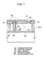
- Fig. 1 is a longitudinal side elevational view showing the structure of a bipolar transistor according to a first embodiment of the present invention.
- This bipolar transistor is an NPN type bipolar transistor including: an emitter electrode which is formed by filling a trench reaching a buried oxide film 101 in the SOI substrate 100 through an interlayer insulating film 20 which is formed between an active region for a device which is formed on an n type SOI (Silicon On Insulator) substrate 100 having an Si layer with 1 to 2 ⁇ m or less thickness and a first level wiring with an electrically conductive film 50 such as an n type polysilicon film; and a uniform p type base layer 70 which is formed along the conductive film 50 thus filled thereon.
- n type SOI Silicon On Insulator
- phosphorus for example is diffused from the conductive film (the n type polysilicon film) 50 into the SOI substrate 100 to form an n type emitter region 60, and an n type collector region 40 is formed on the surface of the SOI substrate 100.
- reference numerals 10, 11 and 12 designates respectively field oxide films
- reference numerals 30 and 31 designates respectively insulating films for isolation each of which is formed by filling the trench with an insulating material
- reference numeral 41 designates a contact hole for a collector
- reference numeral 80 designates a high impurity concentrated region for a base contact.
- a p type emitter electrode is formed by employing a p type SOI substrate, whereby a PNP type transistor may also be formed similarly to the above-mentioned embodiment.
- Fig. 2 is a longitudinal side elevational view showing the structure of a bipolar transistor according to a second embodiment of the present invention.
- This bipolar transistor is an NPN type bipolar transistor including: a collector electrode which is formed by filling a trench reaching a buried oxide film 101 in the SOI substrate 100 through an interlayer insulating film 20 which is formed between the active region for a device which is formed on the n type SOI substrate 100 and the first level wiring with an electrically conductive film 53 such as an n type polysilicon film.
- a p type base region 71 is formed by utilizing the diffusion of the impurities from a p type polysilicon film 72 thereinto.
- n type impurity ions such as arsenic ions are implanted with a sidewall 73 made of an insulating film, which is formed on the sidewall face of the p type polysilicon film 72, as a mask, thereby forming an n type emitter region 61.
- reference numerals 10 and 11 designate respectively field oxide films
- reference numeral 20 designates an interlayer insulating film
- reference numerals 30 and 31 designate respectively insulating films for isolation.
- a p type collector electrode is formed by employing a p type SOI substrate, whereby a PNP type transistor may also be formed similarly to the above-mentioned embodiment.
- Figs. 3a to 3i show, in the order of the processes, the preferred process (method) of manufacturing the bipolar transistor which has been described in the first embodiment of the present invention.
- the field oxide films 10, 11 and 12 are respectively formed on the n type SOI substrate 100 by utilizing the well known process.
- P type impurity ions such as boron ions are implanted into the region, in which the base is intended to be formed, in such a way as to have the concentration by which the ohmic contact can be obtained with a metallic film to form the p type region 80, and also n type impurity ions such as arsenic ions are implanted into the region in which the collector is intended to be formed to form the n type region 40.
- a silicon oxide film for example is deposited to the substrate body by utilizing the CVD method to form the interlayer insulating film 20.
- the trench 51 is formed in such a way as to pass through the interlayer insulating film 20 and the silicon substrate part of the SOI substrate 100 to reach the buried oxide film 101 in the SOI substrate 100.
- Boron is diffused in such a way that its vertical concentration in the trench 51 becomes uniform by utilizing the vapor phase diffusion method or the plasma doping method to form the p type base layer 70.
- the n type polysilicon film 50 which has been doped with phosphorus for example is deposited to fill in the trench 51.
- the unnecessary region of the polysilicon film 50 is removed by utilizing the dry etching method for example to leave the polysilicon film 50 only in the region in which the emitter is intended to be formed which polysilicon film thus left is filled in the trench 51.
- the annealing is carried out in the nitrogen ambient atmosphere to exude phosphorus from the polysilicon film 50 which has been doped with phosphorus to form the n type emitter region 60.
- the contact hole 41 is formed through the interlayer insulating film 20 in order to form the collector electrode, and also a contact hole (not shown) is formed in such a way that the contact with the base region 80 can be obtained therethrough. Thereafter, the metal wiring is formed by utilizing the well known wiring process to complete the process of manufacturing the bipolar transistor.
- Figs. 4a to 4j show, in the order of the processes, the preferred process (method) of manufacturing the bipolar transistor which has been described in the second embodiment of the present invention.
- the field oxide films 10 and 11 are respectively formed on the n type SOI substrate 100 by utilizing the well known process.
- the polysilicon film is deposited and then selectively etched away to form the polysilicon film 72 which has been doped with boron for example.
- the annealing is carried out in the nitrogen ambient atmosphere to diffuse boron from the polysilicon film 72 into the silicon substrate part of the SOI substrate 100 to form the base region 71.
- the sidewall 73 made of a silicon oxide film is formed on the side end face of the polysilicon film 71. In process shown in Fig. 4e
- Arsenic ions for example are implanted to form the emitter region 61.
- the silicon oxide film 20 for example is deposited by utilizing the CVD method.
- the trench 52 is formed.
- the n type polysilicon film 53 which has been doped with phosphorus for example is deposited to fill in the trench 52.
- the polysilicon film 53 is processed by utilizing the dray etching method for example in such a way that only an region which is required for the collector electrode is left.
- the contact hole 62 for the emitter region 61 is formed, and also a contact hole (not shown) is formed in such a way that the contact with the polysilicon film 72 and the base region 71 can be carried out therethrough. Thereafter, the metal wiring is formed by utilizing the well known wiring process to complete the bipolar transistor.
- the processes shown in Figs. 4d and 4e may also be changed into the processes shown in Figs. 5k to 5n.
- the processes shown in Figs. 4a to 4c and the processes shown in Figs. 4f to 4j are not changed at all.
- a silicon oxide film is deposited by utilizing the CVD method or the like and then this silicon oxide film is processed to form the silicon oxide film 74 with which the p type polysilicon layer 72 is covered.
- the etchback is carried out therefor to form the sidewall 73, made of the silicon oxide film, on the side end faces of the p type polysilicon film 72 and the silicon oxide film 74 formed on the p type polysilicon film 72.
- this n type polysilicon film is selectively etched away to leave the necessary part thereof, thereby forming the polysilicon film 63.
- the annealing is carried out in the nitrogen ambient atmosphere for example to diffuse phosphorus from the n type polysilicon film 63, thereby forming the emitter region 63.
- Fig. 6 shows a preferred layout pattern (which is obtained by making the individual mask patterns overlap each other) for the bipolar transistor which was described in the first embodiment of the present invention.
- reference numerals 201 and 202 designate respectively mask patterns which are used to define the active region of the device. The inner part thereof becomes the active region of the device.
- Reference numeral 401 designates a mask pattern which is used to form the collector region
- reference numeral 402 designates a mask pattern which is used to form the contact hole through the interlayer insulating film in order to form the collector region.
- Reference numeral 601 designates a mask pattern which is used to form the high impurity concentrated region with which the contact with the base region is made the ohmic contact and through which the impurity ions having the same conductivity type as that of the impurities in the base region are implanted.
- Reference numerals 602 and 603 designate respectively mask patterns which are used to form the contact holes between the base region and the interlayer insulating film.
- Reference numeral 501 designates a mask pattern which is used to form the trench
- reference numeral 502 designates a mask pattern which is used to process the electrically conductive film filling in the trench.
- Reference numeral 1000 designates a mask pattern which is used to form the trench for isolation.
- a mask pattern is also employed which is used to form the wiring pattern in such a way as for the wiring pattern to become in contact with the mask pattern for the contact holes and the mask pattern which is used to process the electrically conductive film filling in the trench.
- Fig. 7 shows a preferred layout pattern (which is obtained by making the individual mask patterns overlap each other) for the formation of the bipolar transistor which was described in the second embodiment of the present invention.
- reference numerals 201 and 202 designate respectively mask patterns which are used to define the active region of the device. The inner part thereof becomes the active region of the device.
- Reference numerals 703 and 704 designate respectively mask patterns which are used to define the region for the polysilicon film having the same conductivity type as that of the base layer to be formed.
- Reference numeral 701 designates a mask pattern which is used to form the emitter region
- reference numeral 602 designates a mask pattern which is used to form the contact holes through the interlayer insulating film in order to form the emitter region.
- Reference numeral 503 designates a mask pattern which is used to form the trench in which the collector electrode is to be formed
- reference numeral 504 designates a mask pattern which is used to process the electrically conductive film filling in the trench.
- Reference numeral 1000 designates a mask which is used to form the trench for isolation.
- a mask pattern is also employed which is used to form the wiring pattern in such a way as for the wiring pattern to become in contact with the mask pattern for the contact holes and the mask pattern which is used to process the electrically conductive film filling in the trench.
- Fig. 8 is a longitudinal side elevational view showing the structure of a bipolar transistor according to a seventh embodiment of the present invention.
- This bipolar transistor is an NPN type bipolar transistor including: an emitter electrode which is formed by filling a trench reaching a buried oxide film 101 of an n type SOI substrate 100 through an interlayer insulating film 20 formed between an active region of a device, which is formed on the SOI substrate 100, and a first level wiring with an electrically conductive film 50 such as an n type polysilicon film; and a collector electrode which is formed by filling a trench reaching the buried oxide film 101 of the SOI substrate 100 through a field oxide film formed between the active region of the device and the first level wiring, and the interlayer insulating film 20 with an electrically conductive film 51 such as an n type polysilicon film.
- reference numeral 10 designates a field oxide film
- reference numerals 30 and 31 designate respectively insulating films for isolation
- reference numeral 60 designates an n type emitter region
- reference numeral 70 designates a p type base layer
- reference numeral 80 designates a high impurity concentrated region for the base contact.
- n type SOI substrate 100 is employed, it is to be understood that a p type SOI substrate is employed in order to form a p type collector electrode, whereby a PNP type bipolar transistor may also be formed similarly to the above-mentioned embodiments.
- Figs. 9a to 9j show, in the order of the processes, the preferred process of manufacturing the bipolar transistor which has been described in the seventh embodiment of the present invention.
- the field oxide films 10 and 11 are respectively formed on the n type SOI substrate 100.
- Boron ions for example are implanted to form the high impurity concentrated p type region 80.
- the silicon oxide film (the interlayer insulating film) 20 is deposited by utilizing the CVD method for example.
- the trench 51 is formed.
- Boron is diffused by utilizing the vapor phase diffusion method, the plasma doping method or the like to form the p type base region 70.
- the n type polysilicon film 50 which has been doped with phosphorus for example is deposited to fill in the trench.
- the unnecessary region of the polysilicon film 50 is selectively etched away by utilizing the dry etching method for example.
- the trench 52 is formed.
- the unnecessary region of the n type polysilicon film 53 is etched away by utilizing the dry etching for example.
- the annealing is carried out in the nitrogen ambient atmosphere for example to exude phosphorus from the polysilicon film 50 filling in the trench into the silicon substrate part of the SOI substrate 100 to form the n type region 60, thereby completing the bipolar transistor.
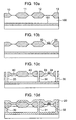
- Figs. 10a to 10h show, in the order of the processes, the preferred process of manufacturing a semiconductor device in which the bipolar transistor which was described in the first embodiment of the present invention and an n-channel MOS transistor are both formed on one chip.
- the field oxide films 10, 11, 12 and 13 are respectively formed on the n type SOI substrate 100.
- a thermal oxide film and a polysilicon film which has been doped with the n type impurities are deposited to be processed by utilizing the dry etching method for example, whereby a gate oxide film 91 and a gate electrode 92 which are the constituent elements of the n-channel MOS transistor are respectively formed.
- Boron ions for example are implanted into the region in which the bipolar transistor is intended to be formed to form the high impurity concentrated p type region 80.
- arsenic ions for example are implanted to form both of the high impurity concentrated n type region 40 for the collector electrode of the bipolar transistor, and a source electrode 93 and a drain electrode 94 of the n-channel MOS transistor.
- trenches 33, 34 and 35 for isolation are respectively formed.
- the silicon oxide film is deposited by utilizing the CVD method for example to fill in the trenches 33, 34 and 35 to form the insulating films for isolation 30, 31 and 32 and also to form the interlayer insulating film 20 between the active region of the device and the first level wiring.
- the interlayer insulating film 20 is processed with a photo resist pattern as a mask to form a groove 55 for the formation of the trench.
- a trench 51 is formed through the silicon substrate part with the interlayer insulating film 20 as a mask.
- Boron ions are implanted by utilizing the vapor phase diffusion method, the plasma doping method or the like to form the base region 70 of the bipolar transistor. In process shown in Fig. 10h
- the processing of removing the unnecessary part of the n type polysilicon film is carried out to form the electrically conductive film 50 within the trench 51.
- the contact holes 41, 95 and 96 for the formation of the collector electrode of the bipolar transistor, and a source electrode and a drain electrode of the n-channel MOS transistor are formed.
- the metal wiring is formed by utilizing the well known wiring process to complete the bipolar transistor.
- the present invention may also be implemented with respect to the bipolar transistor which was described in the second or seventh embodiment similarly to the present embodiment.
- the present invention may also be implemented with respect to a p-channel MOS transistor and a CMOS transistor as well as the n-channel MOS transistor.
- Figs. 11a to 11h show, in the order of the processes, the preferred process of manufacturing a semiconductor device in which the bipolar transistor which was described in the first embodiment of the present invention and a high-voltage withstanding lateral n-channel MOS transistor are both formed on one chip.
- the field oxide films 10, 11, 12, 13 and 14 are respectively formed on the n type SOI substrate 100.
- the thermal oxide film and the polysilicon film which has been doped with n type impurities are deposited to be processed by utilizing the dry etching method for example, whereby the gate oxide film 91 and the gate electrode 92 of the high-voltage withstanding n-channel MOS transistor are both formed.
- the diffusion is carried out at 1100°C for about several tens to about several hundreds minutes to form a deep p type impurity region 95.
- Impurity ions such as boron ions are implanted into the region in which the bipolar transistor is intended to be formed to form a high impurity concentrated p type region 80 and to form a high impurity concentrated n type region 40 for the collector electrode of the bipolar transistor.
- impurity ions such as arsenic ions are implanted into the source region and the drain region of the high-voltage withstanding n-channel MOS transistor to form high impurity concentrated n type regions 98 and 99, respectively.
- Trenches 33, 34 and 35 for isolation are respectively formed.
- a silicon oxide film is deposited by utilizing the CVD method for example to fill in the trenches 33, 34 and 35 to form insulating films for isolation 30, 31 and 32 and to form an interlayer insulating film 20 between the active region of the device and the first level wiring.
- a trench 51 is formed through the silicon substrate part of the SOI substrate 140.
- Boron ions are implanted by utilizing the vapor phase diffusion method, the plasma doping method or the like to form the base region 70 of the bipolar transistor. Thereafter, an n type polysilicon film or the like is deposited to fill in the trench 51 to be processed, thereby forming an n type polysilicon film 50. Then, the annealing is carried out therefor to exude phosphorus from the n type polysilicon film 50 to form the emitter region 60. In addition, contact holes 41, 905 and 906 for the formation of the collector electrode of the bipolar transistor, and the source electrode and the drain electrode of the high-voltage withstanding n-channel MOS transistor are respectively formed.
- the metal wiring is formed by utilizing the well known wiring process to complete the semiconductor device.
- the present invention may also be implemented with respect to the bipolar transistor which was described in the second or seventh embodiment similarly to the present embodiment.
- the present invention may also be implemented with respect to high-voltage withstanding devices such as a high-voltage withstanding p-channel MOS transistor and an IGBT as well as the high-voltage withstanding n-channel MOS transistor.
- the contact position of the collector is set in various ways, whereby the distance of the collector drift region which leads from the emitter electrode to the collector electrode can be set in various ways, and also the withstanding voltage of the bipolar transistor can be controlled depending on only the distance of the drift region.
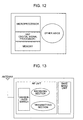
- Fig. 12 is a block diagram showing a configuration of a system LSI.
- a DRAM or an SRAM is employed as a memory unit.
- the bipolar transistor of the present invention is applied to a sense amplifier unit and a decoder circuit unit, whereby both of the low cost and the high speed operation can be realized.
- a driver circuit in which the high driving ability of the bipolar transistor is utilized is selectively used in a circuit, for generating a voltage for a high accuracy reference power source, employing the bipolar transistor or in a part having a large load capacity, whereby the high speed operation of the system LSI can be realized.
- the bipolar transistor of the present invention since for the bipolar transistor of the present invention, only by adding the process of forming a trench electrode between the process of forming an interlayer insulating film and the process of forming a wiring, the high performance bipolar transistor can be realized, the simplification of the process can be realized, the bipolar transistor can be readily manufactured together with the fine MOS transistor, and this configuration can contribute to the promotion of the high performance of the system LSI.
- Fig. 13 is a block diagram showing a configuration of a portable telephone system as one example of a communication system.
- the portable telephones (the apparatuses for communication) can be roughly classified into two parts, i.e., an RF (radio frequency) part and a BB (base band) part.
- RF radio frequency
- BB base band
- the BB part can be realized by the CMOS.
- the promotion of the high frequency in the frequency has advanced in both of the reception unit and the transmission unit, and at the present time, the RF part must process the analog signal having the frequency of several hundreds MHz to several GHz. Then, while at the present time, the compound semiconductor devices employing GaAs or the like are employed, such devices are inexpensive.
- the bipolar transistor of the present invention can also process the analog signal having a frequency of several GHZ.
- the bipolar transistor of the present invention is applied to the RF part, whereby both of the RF part and the BB part can be manufactured on one chip.
- the bipolar transistor of the present invention does not exert an influence on the CMOS manufacturing process at all, the present invention can readily cope with the scale down (shrink) of the CMOSs.
- the bipolar transistors having the different device withstanding voltages can be integrated through the same process, the high performance communication system can be realized between the signal processing unit and the power source unit, and between the analog unit and the digital unit without degrading the mutual characteristics.
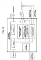
- Fig. 14 is a block diagram showing a configuration of a part of a color television receiver.
- a block diagram of one chip signal processing IC for a television is shown in the frame indicated by a heavy line.
- This IC is an IC for executing all of the analog processings for a small signal except a tuner unit. While since the high speed processing and the high amplification factor are both required for the signal processing in this IC, the signal processing in this IC can be realized by employing the bipolar transistors, the bus decoder, the delay line, the synchronous deflecting processing and the like are realized by employing the MOS transistors.
- the bipolar transistor of the present embodiment is applied to that IC, whereby the digital television receiver of the next generation for which the high speed analog processing is required due to the promotion of the high density of the scanning lines can be readily realized. Also, since the bipolar transistor of the present embodiment is readily manufactured together with the MOS transistor, that IC can be readily manufactured on one chip.
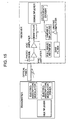
- Fig. 15 is a block diagram showing a configuration of an optical transmission system.
- the high speed analog signal processing is realized by utilizing the compound semiconductor such as GaAs.
- the bipolar transistor of the present embodiment is applied to the analog signal processing, whereby the optical transmission system can be constructed without employing any of the compound semiconductor devices, the promotion of the low cost can be realized.
- the analog signal processing unit can be realized by utilizing the silicon device, each of the transmitter and the receiver can be manufactured on one chip.
- a lateral bipolar transistor which is a match in the device performance for a vertical bipolar transistor can be formed by utilizing an SOI substrate.
- the distance of the collector drift region can be arbitrarily set, and hence an arbitrary-voltage withstanding bipolar transistor can be realized only by changing that distance.
Landscapes
- Bipolar Transistors (AREA)
- Metal-Oxide And Bipolar Metal-Oxide Semiconductor Integrated Circuits (AREA)
- Semiconductor Memories (AREA)
Abstract
A semiconductor device
including a SOI bipolar transistor comprising an emitter electrode
and/or a collector electrode formed by filling
a trench reaching a buried oxide film (101) in an SOI
substrate (100) with an electrically conductive film (50,51,53).
Description
The present invention relates to a semiconductor
device having a lateral bipolar transistor and a method of
manufacturing the same.
In general, a bipolar transistor which is formed
on an Si substrate or an SOI (Silicon On Insulator)
substrate is formed in such a way as to have the vertical
structure. Since the formation of the bipolar transistor
in the vertical structure enables the base width to be
thinned and also enables the junction area between an
emitter and a base to be restricted roughly to the size of
the active region, the high performance can be realized.
However, in order that the bipolar transistor
may be formed in such a way as to have the vertical
structure, an n+ type buried layer becomes essential
thereto. On the contrary, in the case where the SOI
substrate is employed in order to obtain the n type buried
layer, an Si layer in the region in which a device is
intended to be formed is compelled to become thick. Then,
while there have been made a plurality of proposals for
forming a lateral bipolar transistor on the SOI substrate
having a thin Si layer, the process thereof is complicated.
For example, in IEDM (IEDM 93, pp. 75 to 78)
1993, there is proposed a bipolar transistor which is
formed in such a way that an N type collector drift region
is determined on the basis of an oxide film mask; n type
impurity ions having a high concentration are implanted to
form a collector electrode; then, p type impurity ions are
implanted to form a base region; then, the base region is
subjected to the silicon etching with the oxide film, with
which the collector drift region is defined, as a mask to
form a narrow base region; then, n type polysilicon is
deposited to form an emitter electrode. In addition
thereto, a lateral bipolar transistor which is formed on
an SOI substrate is also reported in IEDM 91, pp. 663 to
667.
However, in the structure in which the lateral
bipolar transistor is conventionally formed on the SOI
substrate, the manufacturing process is compelled to be
complicated.
In the light of the foregoing, it is therefore
one object of the present invention to provide a semiconductor
device in which a lateral bipolar transistor which
is a match in the device performance for a vertical
bipolar transistor can be formed through a simple manufacturing
process, and a method of manufacturing the same.
According to one aspect of the present invention,
there is provided a semiconductor device, wherein an electrode
which is formed by filling a trench reaching a
buried oxide film in an SOI substrate with an electrically
conductive film or a metallic film is utilized as an
emitter electrode and/or a collector electrode to simplify
the manufacturing process and to form a lateral bipolar
transistor which is a match in the device performance for
a vertical bipolar transistor.
P type impurity ions for example are implanted
through the trench by utilizing the vapor phase diffusion
method, the plasma doping method, the oblique ion implantation
method or the like, whereby it is possible to form
a very thin base layer which has the vertically uniform
concentration distribution ranging from the surface of the
SOI substrate to the buried oxide film. In addition, for
the formation of an emitter layer, there may also be
adopted the method wherein after the trench has been
filled with n type polysilicon for example, the overall
substrate is exposed to the high temperatures to diffuse n
type impurities from n type polysilicon. In addition,
there may also be adopted the method wherein by the
phosphorus deposition method is utilized which is employed
for a long time as the method of after having formed a
base layer, carrying out doping with phosphorus or the
like, after having formed an emitter region, a metallic
film is filled therein.
In addition, for the formation of an emitter
electrode and a collector electrode of the bipolar
transistor, there is adopted the structure in which the
trench is filled with an electrically conductive semiconductor
film or metal, whereby a voltage can be applied
which is vertically uniform from the surface of the
substrate to the buried oxide film, which leads to the
enhancement of the performance of the lateral bipolar
transistor.
In addition, according to another aspect of the
present invention, after having formed an interlayer
insulating film, an emitter electrode and/or a collector
electrode of the bipolar transistor are/is formed. As a
result, since the above-mentioned processing does not
exert an influence on the fine patterning of MOS transistors
which are formed together with the lateral bipolar
transistors on the SOI substrate, it is possible to form
the lateral bipolar transistors together with the fine MOS
transistors on the SOI substrate. Furthermore, the above-mentioned
processing is carried out after the formation of
the interlayer insulating film, whereby a metallic film
can be employed for the emitter electrode and/or the
collector electrode.
Embodiments of the present invention will
hereinafter be described with reference to the
accompanying drawings. The same or equivalent constituent
means in the preferred embodiments are designated with the
same reference numerals and the repeated description is
omitted here for the sake of simplicity.
Fig. 1 is a longitudinal side elevational view
showing the structure of a bipolar transistor according to
a first embodiment of the present invention.
This bipolar transistor is an NPN type bipolar
transistor including: an emitter electrode which is formed
by filling a trench reaching a buried oxide film 101 in
the SOI substrate 100 through an interlayer insulating
film 20 which is formed between an active region for a
device which is formed on an n type SOI (Silicon On
Insulator) substrate 100 having an Si layer with 1 to 2 µm
or less thickness and a first level wiring with an
electrically conductive film 50 such as an n type
polysilicon film; and a uniform p type base layer 70 which
is formed along the conductive film 50 thus filled thereon.
In the present embodiment, phosphorus for
example is diffused from the conductive film (the n type
polysilicon film) 50 into the SOI substrate 100 to form an
n type emitter region 60, and an n type collector region
40 is formed on the surface of the SOI substrate 100.
By the way, in Fig. 1, reference numerals 10, 11
and 12 designates respectively field oxide films,
reference numerals 30 and 31 designates respectively
insulating films for isolation each of which is formed by
filling the trench with an insulating material, reference
numeral 41 designates a contact hole for a collector, and
reference numeral 80 designates a high impurity concentrated
region for a base contact.
In addition, the contact structure defined
between the base region and a metal wiring will be
described later in a fifth embodiment.
While the present embodiment adopts the structure
employing the n type SOI substrate 100, it is to be
understood that a p type emitter electrode is formed by
employing a p type SOI substrate, whereby a PNP type
transistor may also be formed similarly to the above-mentioned
embodiment.
Fig. 2 is a longitudinal side elevational view
showing the structure of a bipolar transistor according to
a second embodiment of the present invention.
This bipolar transistor is an NPN type bipolar
transistor including: a collector electrode which is
formed by filling a trench reaching a buried oxide film
101 in the SOI substrate 100 through an interlayer
insulating film 20 which is formed between the active
region for a device which is formed on the n type SOI
substrate 100 and the first level wiring with an electrically
conductive film 53 such as an n type polysilicon
film.
In the present embodiment, a p type base region
71 is formed by utilizing the diffusion of the impurities
from a p type polysilicon film 72 thereinto. In addition,
n type impurity ions such as arsenic ions are implanted
with a sidewall 73 made of an insulating film, which is
formed on the sidewall face of the p type polysilicon film
72, as a mask, thereby forming an n type emitter region 61.
By the way, reference numerals 10 and 11 designate
respectively field oxide films, reference numeral 20
designates an interlayer insulating film, and reference
numerals 30 and 31 designate respectively insulating films
for isolation.
While the present embodiment adopts the
structure employing the n type SOI substrate 100, it is to
be understood that a p type collector electrode is formed
by employing a p type SOI substrate, whereby a PNP type
transistor may also be formed similarly to the above-mentioned
embodiment.
Figs. 3a to 3i show, in the order of the
processes, the preferred process (method) of manufacturing
the bipolar transistor which has been described in the
first embodiment of the present invention.
The field oxide films 10, 11 and 12 are
respectively formed on the n type SOI substrate 100 by
utilizing the well known process.
P type impurity ions such as boron ions are
implanted into the region, in which the base is intended
to be formed, in such a way as to have the concentration
by which the ohmic contact can be obtained with a metallic
film to form the p type region 80, and also n type
impurity ions such as arsenic ions are implanted into the
region in which the collector is intended to be formed to
form the n type region 40.
A silicon oxide film for example is deposited to
the substrate body by utilizing the CVD method to form the
interlayer insulating film 20.
The trench 51 is formed in such a way as to pass
through the interlayer insulating film 20 and the silicon
substrate part of the SOI substrate 100 to reach the
buried oxide film 101 in the SOI substrate 100.
Boron is diffused in such a way that its
vertical concentration in the trench 51 becomes uniform by
utilizing the vapor phase diffusion method or the plasma
doping method to form the p type base layer 70.
The n type polysilicon film 50 which has been
doped with phosphorus for example is deposited to fill in
the trench 51.
The unnecessary region of the polysilicon film
50 is removed by utilizing the dry etching method for
example to leave the polysilicon film 50 only in the
region in which the emitter is intended to be formed which
polysilicon film thus left is filled in the trench 51.
The annealing is carried out in the nitrogen
ambient atmosphere to exude phosphorus from the polysilicon
film 50 which has been doped with phosphorus to form
the n type emitter region 60.
The contact hole 41 is formed through the
interlayer insulating film 20 in order to form the collector
electrode, and also a contact hole (not shown) is
formed in such a way that the contact with the base region
80 can be obtained therethrough. Thereafter, the metal
wiring is formed by utilizing the well known wiring
process to complete the process of manufacturing the
bipolar transistor.
Figs. 4a to 4j show, in the order of the
processes, the preferred process (method) of manufacturing
the bipolar transistor which has been described in the
second embodiment of the present invention.
The field oxide films 10 and 11 are respectively
formed on the n type SOI substrate 100 by utilizing the
well known process.
The polysilicon film is deposited and then
selectively etched away to form the polysilicon film 72
which has been doped with boron for example.
The annealing is carried out in the nitrogen
ambient atmosphere to diffuse boron from the polysilicon
film 72 into the silicon substrate part of the SOI
substrate 100 to form the base region 71.
The sidewall 73 made of a silicon oxide film is
formed on the side end face of the polysilicon film 71.
In process shown in Fig. 4e
Arsenic ions for example are implanted to form
the emitter region 61.
The silicon oxide film 20 for example is
deposited by utilizing the CVD method.
The trench 52 is formed.
The n type polysilicon film 53 which has been
doped with phosphorus for example is deposited to fill in
the trench 52.
The polysilicon film 53 is processed by
utilizing the dray etching method for example in such a
way that only an region which is required for the collector
electrode is left.
The contact hole 62 for the emitter region 61 is
formed, and also a contact hole (not shown) is formed in
such a way that the contact with the polysilicon film 72
and the base region 71 can be carried out therethrough.
Thereafter, the metal wiring is formed by utilizing the
well known wiring process to complete the bipolar transistor.
With respect to this manufacturing process, the
processes shown in Figs. 4d and 4e may also be changed
into the processes shown in Figs. 5k to 5n. In this case,
the processes shown in Figs. 4a to 4c and the processes
shown in Figs. 4f to 4j are not changed at all.
After the base region 71 has been formed by
utilizing the diffusion of the impurities from the p type
polysilicon film 72 in the process shown in Fig. 4c, a
silicon oxide film is deposited by utilizing the CVD
method or the like and then this silicon oxide film is
processed to form the silicon oxide film 74 with which the
p type polysilicon layer 72 is covered.
After the silicon oxide film has been deposited
by utilizing the CVD method or the like, the etchback is
carried out therefor to form the sidewall 73, made of the
silicon oxide film, on the side end faces of the p type
polysilicon film 72 and the silicon oxide film 74 formed
on the p type polysilicon film 72.
After an n type polysilicon film which is doped
with phosphorus has been deposited on the overall surface
of the substrate body, this n type polysilicon film is
selectively etched away to leave the necessary part
thereof, thereby forming the polysilicon film 63.
The annealing is carried out in the nitrogen
ambient atmosphere for example to diffuse phosphorus from
the n type polysilicon film 63, thereby forming the
emitter region 63.
Fig. 6 shows a preferred layout pattern (which
is obtained by making the individual mask patterns overlap
each other) for the bipolar transistor which was described
in the first embodiment of the present invention.
In the figure, reference numerals 201 and 202
designate respectively mask patterns which are used to
define the active region of the device. The inner part
thereof becomes the active region of the device. Reference
numeral 401 designates a mask pattern which is used to
form the collector region, and reference numeral 402
designates a mask pattern which is used to form the
contact hole through the interlayer insulating film in
order to form the collector region.
While in the present embodiment, the description
made with reference to the associated figures is omitted,
a mask pattern is also employed which is used to form the
wiring pattern in such a way as for the wiring pattern to
become in contact with the mask pattern for the contact
holes and the mask pattern which is used to process the
electrically conductive film filling in the trench.
Fig. 7 shows a preferred layout pattern (which
is obtained by making the individual mask patterns overlap
each other) for the formation of the bipolar transistor
which was described in the second embodiment of the
present invention.
In the figure, reference numerals 201 and 202
designate respectively mask patterns which are used to
define the active region of the device. The inner part
thereof becomes the active region of the device. Reference
numerals 703 and 704 designate respectively mask patterns
which are used to define the region for the polysilicon
film having the same conductivity type as that of the base
layer to be formed. Reference numeral 701 designates a
mask pattern which is used to form the emitter region, and
reference numeral 602 designates a mask pattern which is
used to form the contact holes through the interlayer
insulating film in order to form the emitter region.
While in the present embodiment, the description
made with reference to the associated figures is omitted,
a mask pattern is also employed which is used to form the
wiring pattern in such a way as for the wiring pattern to
become in contact with the mask pattern for the contact
holes and the mask pattern which is used to process the
electrically conductive film filling in the trench.
Fig. 8 is a longitudinal side elevational view
showing the structure of a bipolar transistor according to
a seventh embodiment of the present invention.
This bipolar transistor is an NPN type bipolar
transistor including: an emitter electrode which is formed
by filling a trench reaching a buried oxide film 101 of an
n type SOI substrate 100 through an interlayer insulating
film 20 formed between an active region of a device, which
is formed on the SOI substrate 100, and a first level
wiring with an electrically conductive film 50 such as an
n type polysilicon film; and a collector electrode which
is formed by filling a trench reaching the buried oxide
film 101 of the SOI substrate 100 through a field oxide
film formed between the active region of the device and
the first level wiring, and the interlayer insulating film
20 with an electrically conductive film 51 such as an n
type polysilicon film.
By the way, reference numeral 10 designates a
field oxide film, reference numerals 30 and 31 designate
respectively insulating films for isolation, reference
numeral 60 designates an n type emitter region, reference
numeral 70 designates a p type base layer, and reference
numeral 80 designates a high impurity concentrated region
for the base contact.
While the present embodiment has the structure
in which the n type SOI substrate 100 is employed, it is
to be understood that a p type SOI substrate is employed
in order to form a p type collector electrode, whereby a
PNP type bipolar transistor may also be formed similarly
to the above-mentioned embodiments.
Figs. 9a to 9j show, in the order of the
processes, the preferred process of manufacturing the
bipolar transistor which has been described in the seventh
embodiment of the present invention.
The field oxide films 10 and 11 are respectively
formed on the n type SOI substrate 100.
Boron ions for example are implanted to form the
high impurity concentrated p type region 80.
The silicon oxide film (the interlayer insulating
film) 20 is deposited by utilizing the CVD method for
example.
The trench 51 is formed.
Boron is diffused by utilizing the vapor phase
diffusion method, the plasma doping method or the like to
form the p type base region 70.
The n type polysilicon film 50 which has been
doped with phosphorus for example is deposited to fill in
the trench.
The unnecessary region of the polysilicon film
50 is selectively etched away by utilizing the dry etching
method for example.
The trench 52 is formed.
After the n type polysilicon film 53 which is
doped with phosphorus for example has been deposited to
fill in the trench, the unnecessary region of the n type
polysilicon film 53 is etched away by utilizing the dry
etching for example.
The annealing is carried out in the nitrogen
ambient atmosphere for example to exude phosphorus from
the polysilicon film 50 filling in the trench into the
silicon substrate part of the SOI substrate 100 to form
the n type region 60, thereby completing the bipolar
transistor.
Figs. 10a to 10h show, in the order of the
processes, the preferred process of manufacturing a
semiconductor device in which the bipolar transistor which
was described in the first embodiment of the present
invention and an n-channel MOS transistor are both formed
on one chip.
The field oxide films 10, 11, 12 and 13 are
respectively formed on the n type SOI substrate 100.
A thermal oxide film and a polysilicon film
which has been doped with the n type impurities are
deposited to be processed by utilizing the dry etching
method for example, whereby a gate oxide film 91 and a
gate electrode 92 which are the constituent elements of
the n-channel MOS transistor are respectively formed.
Boron ions for example are implanted into the
region in which the bipolar transistor is intended to be
formed to form the high impurity concentrated p type
region 80. In addition, arsenic ions for example are
implanted to form both of the high impurity concentrated n
type region 40 for the collector electrode of the bipolar
transistor, and a source electrode 93 and a drain
electrode 94 of the n-channel MOS transistor.
Also, trenches 33, 34 and 35 for isolation are
respectively formed.
The silicon oxide film is deposited by utilizing
the CVD method for example to fill in the trenches 33, 34
and 35 to form the insulating films for isolation 30, 31
and 32 and also to form the interlayer insulating film 20
between the active region of the device and the first
level wiring.
The interlayer insulating film 20 is processed
with a photo resist pattern as a mask to form a groove 55
for the formation of the trench.
After photo resist has been removed, a trench 51
is formed through the silicon substrate part with the
interlayer insulating film 20 as a mask.
Boron ions are implanted by utilizing the vapor
phase diffusion method, the plasma doping method or the
like to form the base region 70 of the bipolar transistor.
In process shown in Fig. 10h
After an n type polysilicon film or the like is
deposited to fill in the trench 51, the processing of
removing the unnecessary part of the n type polysilicon
film is carried out to form the electrically conductive
film 50 within the trench 51. In addition, the contact
holes 41, 95 and 96 for the formation of the collector
electrode of the bipolar transistor, and a source
electrode and a drain electrode of the n-channel MOS
transistor are formed.
Thereafter, the metal wiring is formed by
utilizing the well known wiring process to complete the
bipolar transistor.
While in the present embodiment, the description
has been given with respect to the semiconductor device in
which the bipolar transistor which was described in the
first embodiment of the present invention and the n-channel
MOS transistor are both formed on one chip, the
present invention may also be implemented with respect to
the bipolar transistor which was described in the second
or seventh embodiment similarly to the present embodiment.
In addition, the present invention may also be implemented
with respect to a p-channel MOS transistor and a CMOS
transistor as well as the n-channel MOS transistor.
Figs. 11a to 11h show, in the order of the
processes, the preferred process of manufacturing a
semiconductor device in which the bipolar transistor which
was described in the first embodiment of the present
invention and a high-voltage withstanding lateral n-channel
MOS transistor are both formed on one chip.
The field oxide films 10, 11, 12, 13 and 14 are
respectively formed on the n type SOI substrate 100.
The thermal oxide film and the polysilicon film
which has been doped with n type impurities are deposited
to be processed by utilizing the dry etching method for
example, whereby the gate oxide film 91 and the gate
electrode 92 of the high-voltage withstanding n-channel
MOS transistor are both formed.
After p type impurity ions such as boron ions
have been implanted into the region in which the high-voltage
withstanding n-channel MOS transistor is intended
to be formed, the diffusion is carried out at 1100°C for
about several tens to about several hundreds minutes to
form a deep p type impurity region 95.
Impurity ions such as boron ions are implanted
into the region in which the bipolar transistor is
intended to be formed to form a high impurity concentrated
p type region 80 and to form a high impurity concentrated
n type region 40 for the collector electrode of the
bipolar transistor. In addition, impurity ions such as
arsenic ions are implanted into the source region and the
drain region of the high-voltage withstanding n-channel
MOS transistor to form high impurity concentrated n type
regions 98 and 99, respectively.
A silicon oxide film is deposited by utilizing
the CVD method for example to fill in the trenches 33, 34
and 35 to form insulating films for isolation 30, 31 and
32 and to form an interlayer insulating film 20 between
the active region of the device and the first level wiring.
A trench 51 is formed through the silicon
substrate part of the SOI substrate 140.
Boron ions are implanted by utilizing the vapor
phase diffusion method, the plasma doping method or the
like to form the base region 70 of the bipolar transistor.
Thereafter, an n type polysilicon film or the like is
deposited to fill in the trench 51 to be processed,
thereby forming an n type polysilicon film 50. Then, the
annealing is carried out therefor to exude phosphorus from
the n type polysilicon film 50 to form the emitter region
60. In addition, contact holes 41, 905 and 906 for the
formation of the collector electrode of the bipolar
transistor, and the source electrode and the drain
electrode of the high-voltage withstanding n-channel MOS
transistor are respectively formed.
Thereafter, the metal wiring is formed by
utilizing the well known wiring process to complete the
semiconductor device.
While in the present embodiment, the description
has been given with respect to the semiconductor device in
which the bipolar transistor which was described in the
first embodiment of the present invention and the high-voltage
withstanding n-channel MOS transistor are both
formed on one chip, the present invention may also be
implemented with respect to the bipolar transistor which
was described in the second or seventh embodiment
similarly to the present embodiment. In addition, the
present invention may also be implemented with respect to
high-voltage withstanding devices such as a high-voltage
withstanding p-channel MOS transistor and an IGBT as well
as the high-voltage withstanding n-channel MOS transistor.
With respect to the bipolar transistor according
to the present invention, the contact position of the
collector is set in various ways, whereby the distance of
the collector drift region which leads from the emitter
electrode to the collector electrode can be set in various
ways, and also the withstanding voltage of the bipolar
transistor can be controlled depending on only the
distance of the drift region.
Fig. 12 is a block diagram showing a configuration
of a system LSI. In general, a DRAM or an SRAM is
employed as a memory unit. In this memory unit, the
bipolar transistor of the present invention is applied to
a sense amplifier unit and a decoder circuit unit, whereby
both of the low cost and the high speed operation can be
realized. In addition, a driver circuit in which the high
driving ability of the bipolar transistor is utilized is
selectively used in a circuit, for generating a voltage
for a high accuracy reference power source, employing the
bipolar transistor or in a part having a large load
capacity, whereby the high speed operation of the system
LSI can be realized.
In addition, since for the bipolar transistor of
the present invention, only by adding the process of
forming a trench electrode between the process of forming
an interlayer insulating film and the process of forming a
wiring, the high performance bipolar transistor can be
realized, the simplification of the process can be
realized, the bipolar transistor can be readily manufactured
together with the fine MOS transistor, and this
configuration can contribute to the promotion of the high
performance of the system LSI.
Fig. 13 is a block diagram showing a configuration
of a portable telephone system as one example of a
communication system. The portable telephones (the apparatuses
for communication) can be roughly classified into
two parts, i.e., an RF (radio frequency) part and a BB
(base band) part.
The BB part can be realized by the CMOS. On the
other hand, for the RF part, the promotion of the high
frequency in the frequency has advanced in both of the
reception unit and the transmission unit, and at the
present time, the RF part must process the analog signal
having the frequency of several hundreds MHz to several
GHz. Then, while at the present time, the compound
semiconductor devices employing GaAs or the like are
employed, such devices are inexpensive.
The bipolar transistor of the present invention
can also process the analog signal having a frequency of
several GHZ. Thus, the bipolar transistor of the present
invention is applied to the RF part, whereby both of the
RF part and the BB part can be manufactured on one chip.
In addition, since the bipolar transistor of the present
invention does not exert an influence on the CMOS manufacturing
process at all, the present invention can readily
cope with the scale down (shrink) of the CMOSs.
In addition, according to the structure of the
bipolar transistor of the present invention, since the
bipolar transistors having the different device withstanding
voltages can be integrated through the same process,
the high performance communication system can be realized
between the signal processing unit and the power source
unit, and between the analog unit and the digital unit
without degrading the mutual characteristics.
Fig. 14 is a block diagram showing a configuration
of a part of a color television receiver. In the
figure, a block diagram of one chip signal processing IC
for a television is shown in the frame indicated by a
heavy line. This IC is an IC for executing all of the
analog processings for a small signal except a tuner unit.
While since the high speed processing and the high amplification
factor are both required for the signal
processing in this IC, the signal processing in this IC
can be realized by employing the bipolar transistors, the
bus decoder, the delay line, the synchronous deflecting
processing and the like are realized by employing the MOS
transistors.
Therefore, the bipolar transistor of the present
embodiment is applied to that IC, whereby the digital
television receiver of the next generation for which the
high speed analog processing is required due to the promotion
of the high density of the scanning lines can be
readily realized. Also, since the bipolar transistor of
the present embodiment is readily manufactured together
with the MOS transistor, that IC can be readily manufactured
on one chip.
Fig. 15 is a block diagram showing a configuration
of an optical transmission system. In order to cope
with increasing of the amount of transmission information,
for the optical transmission system is required the high
speed analog signal processing. At the present time, this
analog processing is realized by utilizing the compound
semiconductor such as GaAs.
Since the bipolar transistor of the present
embodiment is applied to the analog signal processing,
whereby the optical transmission system can be constructed
without employing any of the compound semiconductor
devices, the promotion of the low cost can be realized. In
addition, since the analog signal processing unit can be
realized by utilizing the silicon device, each of the
transmitter and the receiver can be manufactured on one
chip.
According to the above-mentioned embodiments of
the present invention, a lateral bipolar transistor which
is a match in the device performance for a vertical
bipolar transistor can be formed by utilizing an SOI
substrate.
In addition, in the bipolar transistor of the
above-mentioned embodiments, the distance of the collector
drift region can be arbitrarily set, and hence an
arbitrary-voltage withstanding bipolar transistor can be
realized only by changing that distance.
Claims (10)
- A semiconductor device including a bipolar transistor comprising: an emitter electrode and/or a collector electrode which is(are) formed by filling a trench(es)(51, 52) which is(are) formed in such a way as to pass through an interlayer insulating film (20) for separating a field oxide film (10, 11, 12) formed on an SOI (Silicon On Insulator) substrate (100) of a first conductivity type and/or an active surface as a region in which a device is intended to be formed from a first layer electrode or electrodes of layers lying thereabove to reach a buried oxide film (101) in said SOI substrate with an electrically conductive film (50) of the same conductivity type as that of said SOI substrate or a metallic film.
- A semiconductor device including a bipolar transistor comprising: a collector electrode and an emitter electrode which are formed by filling trenches (51, 52) which are formed in such a way as to pass through an interlayer insulating film (20) for separating a field oxide film (10, 11, 12) formed on an SOI (Silicon On Insulator) substrate (100) of a first conductivity type and/or an active surface as a region in which a device is intended to be formed from a first layer electrode or electrodes of layers lying thereabove to reach an oxide film (101) in said SOI substrate with an electrically conductive film (50) or a metallic film; and a base layer (70, 71) of a second conductivity type different from said first conductivity type which is formed along the trench (the emitter part), which is formed in such a way as to reach said oxide film in said SOI substrate, from the surface of said SOI substrate to a buried oxide film (101) in said substrate.
- A semiconductor device including a bipolar transistor comprising: an emitter electrode which is formed by filling a trench (51, 52) which is formed in such a way as to pass through an interlayer insulating film (20) for separating a field oxide film (10, 11, 12) formed on an SOI (Silicon On Insulator) substrate (100) of a first conductivity type and/or an active surface as a region in which a device is intended to be formed from a first layer electrode or electrodes of layers lying thereabove to reach an oxide film (101) in said SOI substrate with an electrically conductive film (50) or a metallic film; a base electrode of a second conductivity type different from said first conductivity type which is formed in such a way as to have the vertically uniform concentration distribution along said emitter electrode from the surface of said SOI substrate to said buried oxide film in said SOI substrate; and a collector electrode of said first conductivity type which is formed on the surface of said SOI substrate.
- A semiconductor device including a bipolar transistor: comprising a collector electrode which is formed by filling a trench (51, 52) which is formed in such a way as to pass through an interlayer insulating film (20) for separating a field oxide film (10, 11, 12) formed on an SOI (Silicon On Insulator) substrate (100) of a first conductivity type and/or an active surface as a region in which a device is intended to be formed from a first layer electrode or electrodes of layers lying thereabove to reach an oxide film (101) in said SOI substrate with an electrically conductive film (50) or a metallic film.
- A semiconductor device comprising: a first bipolar transistor including an emitter and a collector regions (40; 60, 61, 62) of a first conductivity type which are formed in the regions of a second conductivity type formed in said SOI substrate of said first conductivity type and which have the structure, as defined in claim 1, on an SOI (Silicon On Insulator) substrate (100) of said first conductivity type; and a second bipolar transistor including an emitter and a collector regions (40; 60, 61, 62) of said second conductivity type which have the structure, as defined in claim 1.
- A semiconductor device comprising: a first bipolar transistor including an emitter and a collector regions of a first conductivity type which have the structure, as defined in claim 1, on an SOI (Silicon On Insulator) substrate (100) of a first conductivity type; and a second bipolar transistor including an emitter and a collector regions of a second conductivity type.
- A method of manufacturing a bipolar transistor, comprising:a first step of forming a trench (51, 52) which passes through an interlayer insulating film (20) for separating a field oxide film (10, 11, 12) formed on an SOI (Silicon On Insulator) substrate (100) of a first conductivity type and an active surface as a region in which a device is intended to be formed from a first layer electrode and electrodes of layers lying thereabove to reach an oxide film (101) in said SOI substrate;a second step of diffusing impurities of a second conductivity type different from said first conductivity type into said SOI substrate through said trench;a third step of diffusing impurities of said first conductivity type into said SOI substrate through said trench; anda fourth step of filling said trench with a film (50) of said first conductivity type or a metallic film.
- A method of manufacturing a semiconductor device, comprising:a first step of forming a trench (51, 52) which passes through an interlayer insulating film (20) for separating a field oxide film (10, 11, 12) formed on an SOI (Silicon On Insulator) substrate (100) of a first conductivity type and an active surface as a region in which a device is intended to be formed from a first layer electrode and electrodes of layers lying thereabove to reach an oxide film (101) in said SOI substrate;a second step of diffusing impurities of a second conductivity type different from said first conductivity type into said SOI substrate through said trench;a third step of diffusing impurities of said first conductivity type into said SOI substrate through said trench; anda fourth step of filling said trench with a film (50) of said first conductivity type or a metallic film.
- A method of manufacturing a bipolar transistor, comprising:a first step of forming a trench (51, 52) which passes through an interlayer insulating film (20) for separating a field oxide film (10, 11, 12) formed on an SOI (Silicon On Insulator) substrate (100) of a first conductivity type and an active surface as a region in which a device is intended to be formed from a first layer electrode and electrodes of layers lying thereabove to reach an oxide film (101) in said SOI substrate;a second step of diffusing impurities of a second conductivity type different from said first conductivity type into said SOI substrate through said trench;a fourth step of filling said trench with a film (50) of said first conductivity type or a metallic film; anda fifth step of exposing the substrate body to high temperatures to diffuse said film of said first conductivity type with which said trench has been filled in said fourth step along said trench.
- A method of manufacturing a semiconductor device, comprising:a first step of forming a trench (51, 52) which passes through an interlayer insulating film (20) for separating a field oxide film (10, 11, 12) formed on an SOI (Silicon On Insulator) substrate (100) of a first conductivity type and an active surface as a region in which a device is intended to be formed from a first layer electrode and electrodes of layers lying thereabove to reach an oxide film (101) in said SOI substrate;a second step of diffusing impurities of a second conductivity type different from said first conductivity type into said SOI substrate through said trench;a fourth step of filling said trench with a film (50) of said first conductivity type or a metallic film; anda fifth step of exposing the substrate body to high temperatures to diffuse said film of said first conductivity type with which said trench has been filled in said fourth step along said trench.
Applications Claiming Priority (2)
| Application Number | Priority Date | Filing Date | Title |
|---|---|---|---|
| JP2000048937 | 2000-02-21 | ||
| JP2000048937A JP2001237249A (en) | 2000-02-21 | 2000-02-21 | Semiconductor device and method of manufacturing the same |
Publications (1)
| Publication Number | Publication Date |
|---|---|
| EP1128441A2 true EP1128441A2 (en) | 2001-08-29 |
Family
ID=18570946
Family Applications (1)
| Application Number | Title | Priority Date | Filing Date |
|---|---|---|---|
| EP00118533A Withdrawn EP1128441A2 (en) | 2000-02-21 | 2000-08-25 | Semiconductor devices comprising a SOI bipolar transistor and corresponding manufacturing methods |
Country Status (4)
| Country | Link |
|---|---|
| US (1) | US6570240B1 (en) |
| EP (1) | EP1128441A2 (en) |
| JP (1) | JP2001237249A (en) |
| KR (1) | KR20010083031A (en) |
Cited By (1)
| Publication number | Priority date | Publication date | Assignee | Title |
|---|---|---|---|---|
| GB2546475A (en) * | 2015-12-16 | 2017-07-26 | Wood John | Ultra lateral extra 3 |
Families Citing this family (7)
| Publication number | Priority date | Publication date | Assignee | Title |
|---|---|---|---|---|
| JP2002305304A (en) * | 2001-04-05 | 2002-10-18 | Toshiba Corp | Power semiconductor device |
| JP4056348B2 (en) * | 2002-10-07 | 2008-03-05 | 株式会社ルネサステクノロジ | Integrated circuit chip module and mobile phone |
| EP1630863B1 (en) * | 2004-08-31 | 2014-05-14 | Infineon Technologies AG | Method of fabricating a monolithically integrated vertical semiconducting device in an soi substrate |
| JP4385007B2 (en) * | 2005-06-08 | 2009-12-16 | 株式会社興研 | High pressure load calculation control method and apparatus |
| JP5452195B2 (en) | 2009-12-03 | 2014-03-26 | 株式会社 日立パワーデバイス | Semiconductor device and power conversion device using the same |
| US9209091B1 (en) | 2011-08-05 | 2015-12-08 | Maxim Integrated Products, Inc. | Integrated monolithic galvanic isolator |
| US9640611B2 (en) * | 2014-03-19 | 2017-05-02 | Texas Instruments Incorporated | HV complementary bipolar transistors with lateral collectors on SOI with resurf regions under buried oxide |
Family Cites Families (4)
| Publication number | Priority date | Publication date | Assignee | Title |
|---|---|---|---|---|
| JP3644980B2 (en) * | 1993-09-06 | 2005-05-11 | 株式会社ルネサステクノロジ | Manufacturing method of semiconductor device |
| JP2654607B2 (en) * | 1994-09-22 | 1997-09-17 | 日本電気株式会社 | Method for manufacturing semiconductor device |
| US5708287A (en) * | 1995-11-29 | 1998-01-13 | Kabushiki Kaisha Toshiba | Power semiconductor device having an active layer |
| JP3075204B2 (en) * | 1997-02-28 | 2000-08-14 | 日本電気株式会社 | Method for manufacturing semiconductor device |
-
2000
- 2000-02-21 JP JP2000048937A patent/JP2001237249A/en active Pending
- 2000-08-25 EP EP00118533A patent/EP1128441A2/en not_active Withdrawn
- 2000-08-29 US US09/649,616 patent/US6570240B1/en not_active Expired - Fee Related
- 2000-09-05 KR KR1020000052286A patent/KR20010083031A/en not_active Withdrawn
Cited By (2)
| Publication number | Priority date | Publication date | Assignee | Title |
|---|---|---|---|---|
| GB2546475A (en) * | 2015-12-16 | 2017-07-26 | Wood John | Ultra lateral extra 3 |
| GB2546475B (en) * | 2015-12-16 | 2020-12-02 | Wood John | Ultra-Lateral Power Transistor amd Driver structures |
Also Published As
| Publication number | Publication date |
|---|---|
| US6570240B1 (en) | 2003-05-27 |
| JP2001237249A (en) | 2001-08-31 |
| KR20010083031A (en) | 2001-08-31 |
Similar Documents
| Publication | Publication Date | Title |
|---|---|---|
| US6815822B2 (en) | BICMOS semiconductor integrated circuit device and fabrication process thereof | |
| US4749661A (en) | Vertical slot bottom bipolar transistor structure | |
| US6927452B2 (en) | Semiconductor device having dual isolation structure and method of fabricating the same | |
| KR101175342B1 (en) | Semiconductor device and method of making semiconductor device comprising multiple stacked hybrid orientation layers | |
| US20020187597A1 (en) | Semiconductor device with vertical MOSFET and method of fabricating same | |
| US6225674B1 (en) | Semiconductor structure and method of manufacture | |
| US20040132234A1 (en) | Semiconductor device having silicon on insulator and fabricating method therefor | |
| US12142686B2 (en) | Field effect transistor | |
| US6414371B1 (en) | Process and structure for 50+ gigahertz transistor | |
| KR100350595B1 (en) | Semiconductor device and process for fabricating the same | |
| US6365448B2 (en) | Structure and method for gated lateral bipolar transistors | |
| US6570240B1 (en) | Semiconductor device having a lateral bipolar transistor and method of manufacturing same | |
| US20080149983A1 (en) | Metal-oxide-semiconductor (mos) varactors and methods of forming mos varactors | |
| JP2007194622A (en) | Area-efficient gated diode structure and method of forming the same | |
| US8530319B2 (en) | Vertical silicide e-fuse | |
| KR100412539B1 (en) | BCD device and method of manufacturing the same | |
| US11322414B2 (en) | Concurrent manufacture of field effect transistors and bipolar junction transistors with gain tuning | |
| US7871881B2 (en) | Method for fabrication of a capacitor, and a monolithically integrated circuit comprising such a capacitor | |
| US12113070B2 (en) | Transistor integration on a silicon-on-insulator substrate | |
| US12396221B2 (en) | Junction field-effect transistors | |
| CN119545835A (en) | Semiconductor device and method for manufacturing the same | |
| JPH10163489A (en) | Semiconductor device and its manufacture | |
| KR20030047513A (en) | Bipolar device and method of fabricating the same |
Legal Events
| Date | Code | Title | Description |
|---|---|---|---|
| PUAI | Public reference made under article 153(3) epc to a published international application that has entered the european phase |
Free format text: ORIGINAL CODE: 0009012 |
|
| AK | Designated contracting states |
Kind code of ref document: A2 Designated state(s): AT BE CH CY DE DK ES FI FR GB GR IE IT LI LU MC NL PT SE |
|
| AX | Request for extension of the european patent |
Free format text: AL;LT;LV;MK;RO;SI |
|
| STAA | Information on the status of an ep patent application or granted ep patent |
Free format text: STATUS: THE APPLICATION HAS BEEN WITHDRAWN |
|
| 18W | Application withdrawn |
Effective date: 20030409 |