EP1126554A2 - Electrical connector - Google Patents
Electrical connector Download PDFInfo
- Publication number
- EP1126554A2 EP1126554A2 EP01102516A EP01102516A EP1126554A2 EP 1126554 A2 EP1126554 A2 EP 1126554A2 EP 01102516 A EP01102516 A EP 01102516A EP 01102516 A EP01102516 A EP 01102516A EP 1126554 A2 EP1126554 A2 EP 1126554A2
- Authority
- EP
- European Patent Office
- Prior art keywords
- contact
- section
- electrical connector
- sections
- connector
- Prior art date
- Legal status (The legal status is an assumption and is not a legal conclusion. Google has not performed a legal analysis and makes no representation as to the accuracy of the status listed.)
- Granted
Links
Images


Classifications
-
- H—ELECTRICITY
- H01—ELECTRIC ELEMENTS
- H01R—ELECTRICALLY-CONDUCTIVE CONNECTIONS; STRUCTURAL ASSOCIATIONS OF A PLURALITY OF MUTUALLY-INSULATED ELECTRICAL CONNECTING ELEMENTS; COUPLING DEVICES; CURRENT COLLECTORS
- H01R13/00—Details of coupling devices of the kinds covered by groups H01R12/70 or H01R24/00 - H01R33/00
- H01R13/02—Contact members
- H01R13/22—Contacts for co-operating by abutting
- H01R13/24—Contacts for co-operating by abutting resilient; resiliently-mounted
- H01R13/2407—Contacts for co-operating by abutting resilient; resiliently-mounted characterized by the resilient means
- H01R13/2428—Contacts for co-operating by abutting resilient; resiliently-mounted characterized by the resilient means using meander springs
Definitions
- the present invention relates to an electrical connector having a contact element that is moved rearwardly by the mating contact element when it is plugged into a mating connector.
- a pair of connectors each have a housing and a contact element with a contact section exposed in the front end of the connector.
- One of the connectors has a flexible section so that when it is plugged with the other connector, the contact element is brought into contact with and moved rearwardly by the mating contact element. Consequently, the contact sections are electrically connected to each other under a contact pressure.
- the contact sections be clean and have low contact resistance.
- the conventional contact sections abut against each other only in the plugging direction, failing to provide the so-called "wiping effect.”
- the contact elements produce too little amounts of sliding contact to provide satisfactory wiping effects.
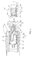
- a pair of connectors 10 and 40 are plugged with each other.
- the connector 40 is mounted on the circuit board P of electronic equipment.
- the connector 10 is plugged into the connector 40.
- the width of the connectors 10 and 40 is made greater than their height.
- the connector 10 comprises a connector body 11 and a cover member 31.
- the connector body 11 comprises a housing body 13 having a plurality of slots or elongated cavities 12, a plurality of contact elements 14 provided in the elongated cavities 12, and a pair of shield plates 15 and 16 provided upper and lower faces of the housing body 13.
- the elongated cavities 12 are arranged at intervals in a direction perpendicular to the sheet and receive the contact elements 14; one in each elongated cavity.
- the housing body 13 has a reduced plugging section 17 for plugging into the mating connector 40 so that each elongate cavity 12 has a wider cavity section 12A and a narrower cavity section 12B.
- a tapered edge 20 and a raised edge 21 are provided at upper and lower edges between the wider and narrower cavity sections 12A and 12B.
- the tapered edge 20 guides the slant section 14D of a contact element 14.
- the contact section 14A of a contact element 14 has a U-shaped form, one leg of which has a free end 14A1 and the other makes a straight section 14A2 which communicates with the slant section 14D.
- the raised edge 21 is provided at such a position as to lift the straight section 14A2 when the straight section 14A2 is moved rearwardly.
- a projection 14A3 provided at an end of the straight section 14A2 is pressed against a wall of the narrower cavity section 12B to determined an initial contact point.
- a pair of protruded sections 18 extend forwardly from opposite sides of the housing body 13 to define a recessed space 19.
- the protruded sections 18 also serve to guides when the connector is plugged into the mating connector 40.
- the lower shield plate 16 is made thicker than the upper shield plate 15 to provide more strength.
- Each contact element 14 has a U-shaped contact section 14A, a connection section 14B projecting rearwardly from the housing body 13, an S-shaped flexible section 14C, and a slant section 14C to connect the flexible section 14C and the contact section 14A.
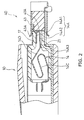
- the front portion of each contact section 14A normally projects into the recessed space 19 but, when the connector 10 is plugged into the mating connector 40, the front end of the contact section 14A is moved backwardly by the contact element of the mating connector to a position which is flush with the bottom of the recessed space 19 (Fig. 2).
- the slant section 14D is moved rearwardly along with the contact section 14A because of the flexible section 14C. That is, the flexible section 14C makes the contact and slant sections 14A and 14C movable.
- the contact sections 14A of all of the contact elements 14 are arranged within the recessed space 19.
- the connector 40 comprises a housing body 42, a plurality of contact elements 41, and a shield plate 43.
- the housing body 42 has a pair of recesses (not shown) on opposite sides thereof to receive the protruded sections 18 of the connector 10.
- a raised section 45 is provided between the recesses to support the contact sections 41A of the contact elements 41. When the raised section 45 is put into the recessed space 19, the contact sections 41A are brought into contact with the contact sections 14A of the connector 10.
- the shield plate 43 surrounds the housing body 42 to provide outer side walls of the recesses. It has a front edge that extends forwardly beyond the front face of the raised section 45 and flares to provide a guide portion 43A.
- a plurality of grooves 42A are provided in the front face of the raised section 45 to receive the contact sections 41A of the contact elements 41. As best shown in Fig. 2, the front face of each contact section 41A is sufficiently high and wide to make contact with the contact section 14A of the mating connector. The width and depth of each groove 42A are made such that the front face of the connector 10 does not make any contact with the contact sections 41A.
- each contact element 41 projects rearwardly from the housing body 42 to provide a connection section 41B which is soldered to a corresponding trace of the circuit board P.
- the shield plate 43 has a pair of legs 43C, which are put into corresponding holes of the circuit board P and soldered for connection.
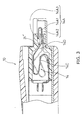
- the raised edge 21 is replaced by raised edge 21' provided on the upper edge between the sloped face 20 and the protruded section 17, and the free ends 14A1 of the contact sections 14A is provided with a projection 14A3, which rides on the raised edge 21' when the contact section 14A is moved rearwardly.
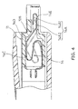
- the inside wall of the narrow cavity section 12B opposed to the straight section 14A2 of the contact element 14 is made flat, and a projection 14E is provided on the straight section 14A2.
- the projection 14E rides on the bottom wall of the narrow cavity section 12B to lift the contact section 14A upwardly.
- the section of the projection 14E closer to the narrow cavity section 12B is sloped slowly so as to facilitate rearward movement of the contact element 14.
- a projection 14E' is provided on the free end 14A1 of the contact section 14A to abut against the inside wall of the narrow cavity section 12B when the contact section 14A is moved rearwardly.
- the inside walls of the narrow cavity section 12B are made flat, making molding of the housing body easy.
- the friction forces of a plurality of contact elements be zero.
- a half of contact elements are arranged on the upper row in a direction and the other half on the lower row in the opposite direction so as to offset the friction forces and provide wiping effects.
- the contact sections of contact elements are arranged alternately in opposite directions so that the friction forces are offset evenly across the width of the connector.
- the raised edges of the housing may be provided on opposite sides.
- the raised edges of Figs. 2 and 3 are formed alternately.
- raised edges or projections are provided on the housing or contact elements to exert forces on the movable sections in a direction perpendicular to the rearward movement of the movable sections of the contact elements so that when the contact sections are brought into contact with the mating contact sections, the movable sections moved by the raised edges or projections produce large sliding movement at the contact sections, increasing the wiping effects.
Landscapes
- Coupling Device And Connection With Printed Circuit (AREA)
- Details Of Connecting Devices For Male And Female Coupling (AREA)
Abstract
Description
Claims (6)
- An electrical connector comprising:a housing having a front opening;at least one connector element provided in the housing which has a contact section provided in said front opening for contact with a mating contact element, a flexible section making said contact section movable in a first direction, and a slant section between said contact and flexible sections; andprojection means for moving said contact section in a second direction perpendicular to said first direction when said contact section is moved in said first direction by said mating contact element.
- An electrical connector according to claim 1, wherein said contact element has a bend in a plane including said first and second directions.
- An electrical connector according to claim 2, wherein said slant section engages with said projection means when said contact section is moved in said first direction.
- An electrical connector according to claim 2, wherein said bends are asymmetrical.
- An electrical connector according to claim 4, wherein said bends are opposed in said second direction.
- An electrical connector according to claim 5, wherein said contact elements are arranged alternately in opposite directions.
Applications Claiming Priority (2)
| Application Number | Priority Date | Filing Date | Title |
|---|---|---|---|
| JP2000031374 | 2000-02-09 | ||
| JP2000031374A JP3634998B2 (en) | 2000-02-09 | 2000-02-09 | Electrical connector |
Publications (3)
| Publication Number | Publication Date |
|---|---|
| EP1126554A2 true EP1126554A2 (en) | 2001-08-22 |
| EP1126554A3 EP1126554A3 (en) | 2003-09-10 |
| EP1126554B1 EP1126554B1 (en) | 2006-11-29 |
Family
ID=18556137
Family Applications (1)
| Application Number | Title | Priority Date | Filing Date |
|---|---|---|---|
| EP01102516A Expired - Lifetime EP1126554B1 (en) | 2000-02-09 | 2001-02-05 | Electrical connector |
Country Status (3)
| Country | Link |
|---|---|
| US (1) | US6312295B2 (en) |
| EP (1) | EP1126554B1 (en) |
| JP (1) | JP3634998B2 (en) |
Cited By (4)
| Publication number | Priority date | Publication date | Assignee | Title |
|---|---|---|---|---|
| FR2849721A1 (en) * | 2003-01-07 | 2004-07-09 | Framatome Connectors Int | Mobile telephone plug in connector for fixed socket has insulating housing with cavities and compression contact terminals contacting socket via secondary terminals |
| EP1852943A1 (en) * | 2006-05-05 | 2007-11-07 | Lumberg Connect GmbH | Contact pressure contact |
| WO2013020948A1 (en) * | 2011-08-09 | 2013-02-14 | Tyco Electronics Amp Gmbh | Electric contact spring, electric spring contact device as well as electric contact zone |
| US9203172B2 (en) | 2013-02-05 | 2015-12-01 | Tyco Electronics Japan G.K. | Electrical connector assembly and electrical connector used therefor |
Families Citing this family (27)
| Publication number | Priority date | Publication date | Assignee | Title |
|---|---|---|---|---|
| WO2002096689A1 (en) * | 2001-05-29 | 2002-12-05 | Tyco Electronics Amp Gmbh | Attachment device for the sun visor of a motor vehicle |
| TW491419U (en) * | 2001-07-20 | 2002-06-11 | Hon Hai Prec Ind Co Ltd | Electrical connector |
| JP4029205B2 (en) | 2001-11-27 | 2008-01-09 | モレックス インコーポレーテッド | Electrical connector |
| CN2660717Y (en) * | 2003-09-23 | 2004-12-01 | 富士康(昆山)电脑接插件有限公司 | Input/output connector |
| TWM251354U (en) * | 2003-09-30 | 2004-11-21 | Hon Hai Prec Ind Co Ltd | I/O connector |
| TWM253091U (en) * | 2003-10-17 | 2004-12-11 | Hon Hai Prec Ind Co Ltd | I/O connector |
| JP3998208B2 (en) * | 2004-06-09 | 2007-10-24 | 日本航空電子工業株式会社 | connector |
| EP2015403B1 (en) * | 2007-07-12 | 2017-05-10 | ODU GmbH & Co KG. | Electrical connector and connection device for such a connector |
| JP5166325B2 (en) * | 2009-03-10 | 2013-03-21 | ミック電子工業株式会社 | Contact pin |
| US9285831B2 (en) | 2009-09-17 | 2016-03-15 | Henge Docks Llc | Docking station for portable electronics |
| US8419479B2 (en) * | 2009-09-17 | 2013-04-16 | Matthew Leigh Vroom | Docking station for an electronic device with improved electrical interface |
| US8251755B2 (en) * | 2010-06-14 | 2012-08-28 | Tyco Electronics Corporation | Connector with a laterally moving contact |
| JP5730063B2 (en) * | 2011-02-21 | 2015-06-03 | 日本圧着端子製造株式会社 | Electrical connector |
| JP5743594B2 (en) * | 2011-02-21 | 2015-07-01 | 日本圧着端子製造株式会社 | Electrical connector |
| US8790139B2 (en) * | 2012-06-22 | 2014-07-29 | Commscope, Inc. Of North Carolina | Communications jacks having sliding contacts and/or contacts having insulative base members |
| JP6002484B2 (en) * | 2012-07-12 | 2016-10-05 | 矢崎総業株式会社 | connector |
| TWI500222B (en) * | 2013-07-12 | 2015-09-11 | Ccp Contact Probes Co Ltd | Connector combination |
| US9927838B2 (en) | 2013-12-31 | 2018-03-27 | Henge Docks Llc | Sensor system for docking station |
| US9650814B2 (en) | 2013-12-31 | 2017-05-16 | Henge Docks Llc | Alignment and drive system for motorized horizontal docking station |
| CN103794902A (en) * | 2014-02-10 | 2014-05-14 | 连展科技电子(昆山)有限公司 | Electric connector with integrally-formed terminals |
| JP6512812B2 (en) * | 2014-12-12 | 2019-05-15 | 宏致電子股▲ふん▼有限公司Aces Electronics Co.,Ltd. | connector |
| US9811118B2 (en) | 2015-10-23 | 2017-11-07 | Henge Docks Llc | Secure assembly for a docking station |
| US9575510B1 (en) | 2015-10-23 | 2017-02-21 | Matthew Leigh Vroom | Precision docking station for an electronic device having integrated retention mechanism |
| US9727084B2 (en) | 2015-10-23 | 2017-08-08 | Henge Docks Llc | Drivetrain for a motorized docking station |
| US9979112B2 (en) * | 2016-03-29 | 2018-05-22 | Aces Electronics Co., Ltd. | Press-type connector |
| US10365688B1 (en) | 2018-04-19 | 2019-07-30 | Henge Docks Llc | Alignment sleeve for docking station |
| CN114447660A (en) * | 2022-03-16 | 2022-05-06 | 上海航天科工电器研究院有限公司 | A terminal and connector |
Family Cites Families (10)
| Publication number | Priority date | Publication date | Assignee | Title |
|---|---|---|---|---|
| US4940432A (en) * | 1989-09-08 | 1990-07-10 | Amp Incorporated | Contact element for test socket for flat pack electronic packages |
| US5030121A (en) * | 1990-02-13 | 1991-07-09 | Thomas & Betts Corporation | Electrical connector with contact wiping action |
| US5259769A (en) * | 1992-09-29 | 1993-11-09 | Molex Incorporated | Electrical connector with preloaded spring-like terminal with improved wiping action |
| GB2276285B (en) * | 1992-11-11 | 1996-03-06 | Elco Europ Ltd | Electrical connector |
| DE19501651A1 (en) * | 1995-01-18 | 1996-07-25 | Siemens Ag | Electrical connector for contacting a device provided with flat contacts, in particular a mobile telephone handset |
| US5716230A (en) * | 1995-06-02 | 1998-02-10 | Molex Incorporated | Surface engageable electrical connector |
| JPH09259964A (en) * | 1996-03-22 | 1997-10-03 | Kel Corp | Surface contact connector |
| JP3351999B2 (en) * | 1997-08-28 | 2002-12-03 | ヒロセ電機株式会社 | Electrical connector |
| GB9804333D0 (en) * | 1998-02-27 | 1998-04-22 | Amp Great Britain | Device-to-board electrical connector |
| EP0969560A1 (en) * | 1998-07-02 | 2000-01-05 | Framatome Connectors International | Facial contact for a connector for accessory for a mobile telephone |
-
2000
- 2000-02-09 JP JP2000031374A patent/JP3634998B2/en not_active Expired - Fee Related
-
2001
- 2001-01-24 US US09/768,164 patent/US6312295B2/en not_active Expired - Fee Related
- 2001-02-05 EP EP01102516A patent/EP1126554B1/en not_active Expired - Lifetime
Cited By (7)
| Publication number | Priority date | Publication date | Assignee | Title |
|---|---|---|---|---|
| FR2849721A1 (en) * | 2003-01-07 | 2004-07-09 | Framatome Connectors Int | Mobile telephone plug in connector for fixed socket has insulating housing with cavities and compression contact terminals contacting socket via secondary terminals |
| WO2004066450A1 (en) * | 2003-01-07 | 2004-08-05 | Fci | Plug connector equipped with compression contact terminals |
| US7144278B2 (en) | 2003-01-07 | 2006-12-05 | Fci | Plug connector equipped with compression contact terminals |
| EP1852943A1 (en) * | 2006-05-05 | 2007-11-07 | Lumberg Connect GmbH | Contact pressure contact |
| CN100589285C (en) * | 2006-05-05 | 2010-02-10 | 伦伯格连接器有限公司 | Pressure contact |
| WO2013020948A1 (en) * | 2011-08-09 | 2013-02-14 | Tyco Electronics Amp Gmbh | Electric contact spring, electric spring contact device as well as electric contact zone |
| US9203172B2 (en) | 2013-02-05 | 2015-12-01 | Tyco Electronics Japan G.K. | Electrical connector assembly and electrical connector used therefor |
Also Published As
| Publication number | Publication date |
|---|---|
| US20010012734A1 (en) | 2001-08-09 |
| EP1126554B1 (en) | 2006-11-29 |
| EP1126554A3 (en) | 2003-09-10 |
| JP3634998B2 (en) | 2005-03-30 |
| US6312295B2 (en) | 2001-11-06 |
| JP2001223049A (en) | 2001-08-17 |
Similar Documents
| Publication | Publication Date | Title |
|---|---|---|
| EP1126554B1 (en) | Electrical connector | |
| US4708415A (en) | Electrical connectors | |
| KR101020120B1 (en) | Electrical connector jack | |
| US4118094A (en) | Zero-entry force connector | |
| KR0110997Y1 (en) | Connector | |
| EP1124290A2 (en) | Electrical connector | |
| CN104838543B (en) | Female end | |
| EP3413398B1 (en) | Multi-contact connector | |
| US7004792B2 (en) | Electrical connector | |
| US6394841B1 (en) | Electric connector having shield plates | |
| US20190229455A1 (en) | Connector | |
| EP2515382A1 (en) | Electrical connectors and receptacle assemblies having retention inserts | |
| US7491078B2 (en) | Stacked electrical connector | |
| FI74364B (en) | WAREHOUSE PROFILERS ELEKTRISK KOPPLINGSINSTALLATION. | |
| EP0488349A2 (en) | Connector with contact spacer plate having tapered channels | |
| FI67458C (en) | ELEKTRISKT KONTAKTDON MED STICKKONTAKT OCH STICKDOSA OCH FOERFARANDE FOER DESS FRAMSTAELLNING | |
| US5194022A (en) | Elecrical connector | |
| US7086893B2 (en) | Electrical connector | |
| KR100387378B1 (en) | Thin connector | |
| US7980864B2 (en) | Connector for flexible printed circuit board | |
| US7559792B2 (en) | Connector with easily replacement of a slider | |
| EP1441418B1 (en) | Ribbon cable connector | |
| JPH0477429B2 (en) | ||
| US4700998A (en) | Multiple contact connector having a low insertion force | |
| US20090298345A1 (en) | Connector |
Legal Events
| Date | Code | Title | Description |
|---|---|---|---|
| PUAI | Public reference made under article 153(3) epc to a published international application that has entered the european phase |
Free format text: ORIGINAL CODE: 0009012 |
|
| AK | Designated contracting states |
Kind code of ref document: A2 Designated state(s): AT BE CH CY DE DK ES FI FR GB GR IE IT LI LU MC NL PT SE TR |
|
| AX | Request for extension of the european patent |
Free format text: AL;LT;LV;MK;RO;SI |
|
| PUAL | Search report despatched |
Free format text: ORIGINAL CODE: 0009013 |
|
| AK | Designated contracting states |
Kind code of ref document: A3 Designated state(s): AT BE CH CY DE DK ES FI FR GB GR IE IT LI LU MC NL PT SE TR |
|
| AX | Request for extension of the european patent |
Extension state: AL LT LV MK RO SI |
|
| RIC1 | Information provided on ipc code assigned before grant |
Ipc: 7H 01R 13/24 B Ipc: 7H 01R 13/22 A |
|
| 17P | Request for examination filed |
Effective date: 20031025 |
|
| 17Q | First examination report despatched |
Effective date: 20031121 |
|
| AKX | Designation fees paid |
Designated state(s): FI GB |
|
| REG | Reference to a national code |
Ref country code: DE Ref legal event code: 8566 |
|
| GRAP | Despatch of communication of intention to grant a patent |
Free format text: ORIGINAL CODE: EPIDOSNIGR1 |
|
| RIN1 | Information on inventor provided before grant (corrected) |
Inventor name: FUJIOKA, TORU,C/O HIROSE ELECTRIC CO., LTD. Inventor name: NISHIMATSU, NORIMASA, |
|
| GRAS | Grant fee paid |
Free format text: ORIGINAL CODE: EPIDOSNIGR3 |
|
| GRAA | (expected) grant |
Free format text: ORIGINAL CODE: 0009210 |
|
| AK | Designated contracting states |
Kind code of ref document: B1 Designated state(s): FI GB |
|
| REG | Reference to a national code |
Ref country code: GB Ref legal event code: FG4D |
|
| PGFP | Annual fee paid to national office [announced via postgrant information from national office to epo] |
Ref country code: GB Payment date: 20070109 Year of fee payment: 7 |
|
| PGFP | Annual fee paid to national office [announced via postgrant information from national office to epo] |
Ref country code: FI Payment date: 20070202 Year of fee payment: 7 |
|
| PLBE | No opposition filed within time limit |
Free format text: ORIGINAL CODE: 0009261 |
|
| STAA | Information on the status of an ep patent application or granted ep patent |
Free format text: STATUS: NO OPPOSITION FILED WITHIN TIME LIMIT |
|
| 26N | No opposition filed |
Effective date: 20070830 |
|
| GBPC | Gb: european patent ceased through non-payment of renewal fee |
Effective date: 20080205 |
|
| PG25 | Lapsed in a contracting state [announced via postgrant information from national office to epo] |
Ref country code: FI Free format text: LAPSE BECAUSE OF NON-PAYMENT OF DUE FEES Effective date: 20080305 |
|
| PG25 | Lapsed in a contracting state [announced via postgrant information from national office to epo] |
Ref country code: GB Free format text: LAPSE BECAUSE OF NON-PAYMENT OF DUE FEES Effective date: 20080205 |