EP1126551A2 - Connector for module - Google Patents
Connector for module Download PDFInfo
- Publication number
- EP1126551A2 EP1126551A2 EP00118666A EP00118666A EP1126551A2 EP 1126551 A2 EP1126551 A2 EP 1126551A2 EP 00118666 A EP00118666 A EP 00118666A EP 00118666 A EP00118666 A EP 00118666A EP 1126551 A2 EP1126551 A2 EP 1126551A2
- Authority
- EP
- European Patent Office
- Prior art keywords
- module
- connector
- metallic cover
- connection position
- connector body
- Prior art date
- Legal status (The legal status is an assumption and is not a legal conclusion. Google has not performed a legal analysis and makes no representation as to the accuracy of the status listed.)
- Withdrawn
Links
Images







Classifications
-
- H—ELECTRICITY
- H01—ELECTRIC ELEMENTS
- H01R—ELECTRICALLY-CONDUCTIVE CONNECTIONS; STRUCTURAL ASSOCIATIONS OF A PLURALITY OF MUTUALLY-INSULATED ELECTRICAL CONNECTING ELEMENTS; COUPLING DEVICES; CURRENT COLLECTORS
- H01R13/00—Details of coupling devices of the kinds covered by groups H01R12/70 or H01R24/00 - H01R33/00
- H01R13/46—Bases; Cases
- H01R13/514—Bases; Cases composed as a modular blocks or assembly, i.e. composed of co-operating parts provided with contact members or holding contact members between them
-
- H—ELECTRICITY
- H01—ELECTRIC ELEMENTS
- H01R—ELECTRICALLY-CONDUCTIVE CONNECTIONS; STRUCTURAL ASSOCIATIONS OF A PLURALITY OF MUTUALLY-INSULATED ELECTRICAL CONNECTING ELEMENTS; COUPLING DEVICES; CURRENT COLLECTORS
- H01R12/00—Structural associations of a plurality of mutually-insulated electrical connecting elements, specially adapted for printed circuits, e.g. printed circuit boards [PCB], flat or ribbon cables, or like generally planar structures, e.g. terminal strips, terminal blocks; Coupling devices specially adapted for printed circuits, flat or ribbon cables, or like generally planar structures; Terminals specially adapted for contact with, or insertion into, printed circuits, flat or ribbon cables, or like generally planar structures
- H01R12/70—Coupling devices
- H01R12/82—Coupling devices connected with low or zero insertion force
- H01R12/83—Coupling devices connected with low or zero insertion force connected with pivoting of printed circuits or like after insertion
Definitions
- the present invention belongs to a technical field of connector for module (hereinafter it may be simply referred to as connector) that is used for a module wherein semiconductor chips are mounted on a rectangular board and conductive pads are provided on a front edge of the board (hereinafter simply referred to as module).
- the present invention relates to countermeasures against heat, electromagnetic waves, etc. to which a connector for module is exposed.
- Modules of this kind include those in which semiconductor chips such as semiconductor memories are mounted.
- a module connector is used extensively, which connects a module of this kind to a printed circuit board such as a mother board in a position wherein the board surface of the module is approximately parallel to the printed circuit board.
- This connector has an approximately U-shaped form to correspond to the front side, left side and right side of the module, respectively.
- a receiving part of the connector corresponding to the front side is provided with a groove that will receive the front side of the module.
- the groove is provided with contacts that will contact conductive pads while allowing the conductive pads to move in a direction of insertion/withdrawal when the module is in an insertion/withdrawal position in which the rear side thereof is lifted more in comparison with its level in the connection position.
- Two arms of the connector corresponding to the left side and the right side of the module are arranged so that their top ends can undergo elastic deformation leftward and rightward, respectively, and each arm is provided with a engaging claw on the inner side of the top end thereof.
- the connector is mounted on the printed circuit board by soldering the solder tails of the contacts onto the printed circuit board and, when necessary, fixing its arms on the printed circuit board.
- the top ends of the arms When the left side and the right side are pressed against the arms, the top ends of the arms will undergo elastic deformation outward and the engaging claws will fit into the left side and the right side of the module. As a result, the module will be retained in the connection position.
- the top ends of the arms are made by fingers to undergo elastic deformation outward to release the engaging claws from the module.
- the rear side of the module will be lifted by the elastic recovering forces of the contacts and the module will be shifted from the connection position into the insertion/withdrawal position. Thus the module can be withdrawn from the receiving part of the connector.
- One object of the present invention is to prevent defective connection and disconnection of the module due to thermal load on the connector body and its elastic deformation by reinforcing the connector body with a metallic cover, and to reduce effects of electromagnetic waves or the like on the connector for module and the module and keep the operation of the circuit stable by covering and shielding the connector with the metallic cover.
- the connector for module is a connector for module that connects a module, which has a semiconductor chip mounted on a rectangular board and has a conductive pad on the front side of the board, to a printed circuit board in a position wherein the board plane is approximately parallel to the printed circuit board.
- This connector for module comprises:
- This connector for module is mounted on a printed circuit board by, for example, soldering the solder tail of the contact onto the printed circuit board and, when necessary, fixing the supporting part onto the printed circuit board.
- the connector body even if the connector is subjected to thermal load from the semiconductor chip, as the connector body is reinforced by the metallic cover and as the thermal load to the connector body is reduced by the heat-dissipating effect of the metallic cover, the connector body will be hardly deformed. Furthermore, as the retaining structure is designed to sandwich the module between the metallic cover and the supporting part, even if the connector is subjected to thermal loads, the retaining force for the module will be hardly affected. Thus the connector can retain the module reliably. Moreover, as the connector body has no parts that are subjected to elastic deformation by manipulation, the connector body will not be damaged. Thus the module can be retained in the connection position reliably.
- the cover covers the connector body and the module, the cover exhibits its shielding function to reduce the effects of electromagnetic waves or the like on the connector for module and the module. Thus the stable operation of the circuit can be maintained.
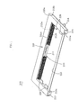
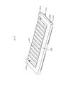
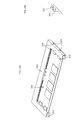
- Fig. 1 is a perspective view showing the first embodiment of the connector.
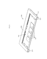
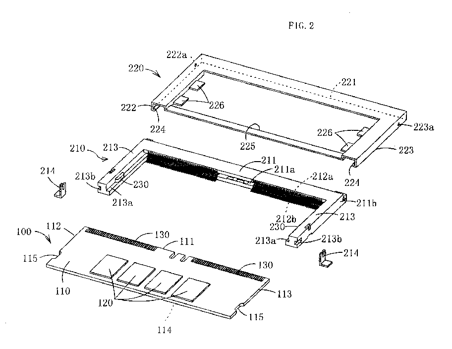
- Fig. 2 is a perspective view showing the first embodiment of the connector, which is disassembled into a connector body and a metallic cover, together with a module.
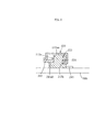
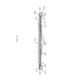
- Fig. 3A is a sectional view showing the first embodiment of the connector with the module being kept in the insertion/withdrawal position.
- Fig. 3B is a partially magnified view of Fig. 3A.
- Fig. 4A is a sectional view of the first embodiment of the connector with the module being kept in the connection position.
- Fig. 4B is a partially magnified view of Fig. 4A.
- Fig. 5 is a perspective view showing the first embodiment of the connector with the module fitted.
- Fig. 6 is a sectional view of one supporting part, which is in the state of Fig. 3, along a plane that faces the front and the rear.
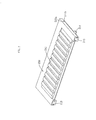
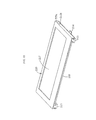
- Fig. 7 is a perspective view of the second embodiment of the connector.
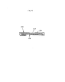
- Fig. 8 is a sectional view of the second embodiment of the connector with a module fitted along a place that faces the front and the rear.
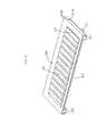
- Fig. 9 is a perspective view of the third embodiment of the connector.
- Fig. 10 is a perspective view showing the fourth embodiment of the connector with a module fitted.
- Fig. 11 is a sectional view of the fourth embodiment of the connector with the module fitted along a plane that faces the front and the rear.
- Fig. 12 is a perspective view of the fifth embodiment of the connector with a module fitted.
- Fig. 13 is a sectional view of the fifth embodiment of the connector with the module fitted along a plane that faces the front and the rear.
- Fig. 14 is a perspective view showing the sixth embodiment of the connector with a module fitted.
- Fig. 15 is a sectional view of the sixth embodiment of the connector with the module fitted along a plane that faces the front and the rear.
- Fig. 16 is a perspective view showing that a heat sink is being assembled with the metallic cover of the sixth embodiment of the connector.
- Fig. 17 is an exploded perspective view of the seventh embodiment of the connector.
- Fig. 18A and Fig. 18B show the connector body of the seventh embodiment of the connector with its metallic cover covering the connector body.
- Fig. 18A is a perspective view
- Fig. 18B is a magnified view of a protrusion of the connector body and a guide groove of the cover.
- Fig. 19A and Fig. 19B show the connector body of the seventh embodiment of the connector and the metallic cover being engaged to the connector body.
- Fig. 19A is a perspective view
- Fig. 19B is a magnified view of a protrusion of the connector body and a guide groove of the cover.
- Fig. 20 is a perspective view showing the eighth embodiment of the connector. Prongs of the metallic cover are being put into holes in the stopping wall.
- Fig. 21 is a perspective view showing the eighth embodiment of the connector. Prongs of the metallic cover are in the holes of the stopping wall.
- Fig. 22 is a perspective view showing the eighth embodiment of the connector with a module fitted.
- Fig. 23 is a sectional view of the eighth embodiment of the connector with the prongs of the metallic cover being in the holes of the stopping wall along a plane that faces the right and the left.
- Fig. 1 through Fig. 6 show the first embodiment of the connector.
- 100 denotes a module.
- the module 100 is provided with a rectangular board 110, on which semiconductor chips 120 such as semiconductor memories are mounted, and conductive pads 130, which are connected to the above-mentioned semiconductor chips 120, etc., are provided on the front side 111 of the board 110.
- the conductive pads 130 are made of conductors and are provided on the face and the back of the board 110.
- the present invention covers a module wherein conductive pads are provided only on the face of the front side of the board, and a module wherein conductive pads are provided only on the back of the front side of the board.
- the marks that are used for the front side, side faces, bottom, etc. of the board 110 are also used for the front side, side faces, bottom, etc. of the module 100.
- the connector 200 denotes a connector for module that connects the above-mentioned module 100 to a printed circuit board 300 such as a mother board.
- the module 100 is fitted in the connector 200 in a position in which the plane of the module 100 is approximately parallel to the printed circuit board 300.
- insertion of the module 100 into the connector 200 and its withdrawal from the connector 200 are made, as shown in Fig. 3A and Fig. 3B, in the insertion/withdrawal position wherein the rear side of the module 100 is raised more than in the connection position and the plane of the module 100 is oblique to the printed circuit board 300.
- the connector 200 is provided with a connector body 210.
- This connector body 210 has a receiving part 211 that extends along the front side 111 of the module 100 being in the connection position, and supporting parts 213 that extend rearward from the receiving part 211 to support the left side 112, the right side 113 and the bottom 114 of the module 100 being in the connection position.
- the rear of the receiving part 211 is provided with a groove 211a into which the front side 111 of the module 100 is to be inserted.
- This groove 211a is provided with contacts 212a, 212b, which contact the conductive pads 130 on both the face and back of the module 100 being in the insertion/withdrawal position while allowing the module 100 to shift in a direction of insertion/withdrawal thereof.
- the contacts 212a, 212b are arranged on an upper side and a lower side in the groove 211a, and the contacts 212b on the lower side are staggered rearward relative to the contacts 212a on the upper side. As shown in Fig. 3A and Fig.
- the module 100 is allowed to shift in the insertion/withdrawal direction when it is in the insertion/withdrawal position.
- Fig. 4A and Fig4B when the module 100 is set in the connection position, the conductive pads 130 and the contacts 212a, 212b will contact with each other.
- contacts may be provided only on the upper side.
- contacts may be provided only on the lower side.
- supporting parts 213 are two, one at the left and the other at the right.
- the two supporting parts 213 extend rearward along the left side and the right side of the module 100, respectively.
- a stepped part 213a is formed on the inner side of the above-mentioned supporting members 213.
- the stepped parts 213a have corners that have an L-shape or an inverted-L-shape when seen from the rear.
- the left and right vertical faces 213aa of the stepped parts 213a support the left side 112 and the right side 113 of the module 100 being in the connection position, and the horizontal faces 213ab support the bottom 114 of the module 100 in the connection position.
- reinforcing tabs 214 being made of, for example, a metal, are fixed to the supporting parts 213. These reinforcing tabs 214 are fixed onto the printed circuit board 300 by soldering, etc.
- the present invention includes an embodiment wherein the supporting part is not divided into the left and right ones but the supporting part is formed integrally and extends rearward from the receiving part along the left side, the right side and the bottom of the module being in the connection position.
- the above-mentioned supporting member has a stepped part that looks a concave when seen from the rear, and the right and left vertical faces of this stepped part receive the left side 112 and the right side 113 of the module being in the connection position, and the horizontal face between the left and right vertical faces support the bottom of the module being in the connection position.
- This connector 200 is provided with a metallic cover 220.
- This metallic cover 220 covers the connector body 210 and is engaged to it, and the metallic cover 220 and the supporting parts 213 sandwich the module 100 to retain it in the connection position.
- a front face supporting part 221, a left side supporting part 222 and the right side supporting part 223 hang from the front edge, left edge and right edge of the metallic cover 220 along the front of receiving part 211, the left side and the right side of the supporting parts 213, respectively.
- provision of the front supporting part 221 is discretionary. It, however, is preferable to provide the front supporting part 221 so as to enhance the shielding effect.
- the metallic cover 220 is hinged to the receiving part 211 at the front, and this allows the metallic cover 220 to lift its rear end.
- the hinged connection is realized by, for example, fixing cylindrical protrusions 211b on the left side and the right side of the receiving part 211 and making these protrusions 211b pierce holes 222a, 223a that are opened in the left side supporting part 222 and the right side supporting part 223 of the metallic cover 220.
- Securing hooks 224 are formed at the rear ends of the left side supporting part 222 and the right side supporting part 223 of the metallic cover 220 by, for example, bending the lower ends inward.
- a window 225 is opened in the center of the metallic cover 220 to expose semiconductor chips 120 of the module 100 being in the connection position.
- Tabs 226 are provided on the inner edges of the window 225 so that the tabs 226 contact the top of the board 110 of the module 100 being in the connection position.
- the tabs 226 and a part that is on the rear side of the window 225 of the metallic cover 220 and is lower than the rest are in contact with the module 100, and this contacting parts transmit the sandwiching force of the metallic cover 220 to the module 100.
- the contacting part for the module 100 may be set at any part or parts of the metallic cover 220.
- the present invention includes an embodiment wherein there is no rear side of the inner edge of the window thus the window is open to the rear.
- the connector body 210 or the metallic cover 220 is provided with a positioning mechanism that will position the module 100 in the front-rear direction when the module 100 comes into the connection position.
- positioning protrusions 230 protruding inward are provided on the vertical faces 213a of the stepped parts 213a of the supporting parts 213.
- the positioning protrusions may be provided on the metallic cover.
- the connector for module of the first embodiment is mounted on a printed circuit board 300 by, for example, soldering the solder tails of contacts 212a, 212b onto the printed circuit board 300 and fixing the supporting parts 213 to the printed circuit board with reinforcing tabs 214, etc. when required.
- the module 100 is set in the insertion/withdrawal position as shown in Fig. 3A and Fig. 3B, and the front side 111 is inserted into the groove 211a of the receiving part 211. As a result, the front side 111 will be inserted between the contacts 212a, 212b.
- the metallic cover 220 is placed over the module 100 and pressed downward.
- the module 100 will be sandwiched between the supporting members 213 and the metallic cover 220 and kept in the connection position.
- positioning of the module 100 in its top-bottom direction is effected by the metallic cover 220 and the horizontal faces 213ab of the supporting members 213, and positioning of the module in its left-right direction is effected by the left and right vertical faces 213aa of the supporting members 213; thus the module 100 is kept in the connection position.
- the metallic cover 220 is pulled up to undone the engagement to the connector body 210.
- the rear side of the module 100 will be lifted up by the elastic restoring forces of the contacts 212a, 212b and shifted from the connection position into the insertion/withdrawal position. Then the module 100 can be withdrawn from the contacts 212a, 212b.
- the connector body 210 even when the connector 200 is exposed to thermal loads of the semiconductor chips 120, the connector body 210 will be hardly deformed because the connector body 210 is reinforced by the metallic cover 220 and the thermal load to the connector body 210 is reduced by the heat dissipating effect of the metallic cover 220.
- the retention structure is designed to sandwich the module 100 between the metallic cover 220 and the supporting parts 213, the forces for retaining the module 100 will be hardly affected even if the retention structure is subjected to thermal loads. Thus the module 100 can be retained reliably. Further, as the connector body 210 has no parts that are to be elastically deformed by manipulation, the connector body 210 will not be damaged by manipulation and the module 100 will be kept in the connection position reliably.
- the metallic cover 220 covers the conductive members such as the contacts 212a, 212b of the connector body 210 and the conductive pads 130 of the module 100 to exhibit its shielding function, effects of any electromagnetic waves, etc. on the connector 200 and the module 100 will be reduced, and in turn, the operation of the circuits will be maintained stably.
- the metallic cover 220 may be arranged to come into contact with the reinforcing tabs 214 when the metallic cover 220 is engaged to the connector body 210. In this way, a circuit will be completed, which grounds the metallic cover 220 via the reinforcing tabs 214. This can enhance the shielding performance of the metallic cover 220.
- the present invention include all embodiments wherein the connector is provided with a metallic cover that is placed over and engaged to the connector body on the module side.
- the metallic cover 220 is hinged to the receiving part 211 at the front thereof so that the rear end of the metallic cover 220 can be lifted up, the metallic cover 220 will be engaged to the connector body 210 when the rear end of the metallic cover 220 is pushed down, and the metallic cover 220 will be disconnected from the connector body 210 when the rear end of the metallic cover 220 is pushed up.
- shifting of the module 100 between the insertion/withdrawal position and the connection position can be done easily with a single touch.
- the present invention includes embodiments wherein no positioning mechanism is provided for positioning the module in the front-rear direction when the module is get into the connection position.
- the connector body 210 or the metallic cover 220 is provided with a positioning mechanism of this kind 230, the module 100 will be kept more accurately in the connection position since the positioning of the module 100 in the up-down direction will be made by the metallic cover 220 and the horizontal faces 213ab of the supporting members 213, the positioning of the module 100 in the left-right direction will be made by the vertical faces 213aa of the supporting members 213, and in addition to them, positioning in the front-rear direction will be made by the positioning mechanism 230.
- Fig. 7 and Fig. 8 show the second embodiment.
- a window 225 is opened in the metallic cover 220, which exposes the semiconductor chips 120 of the module 100 being kept in the connection position.
- a heat sink 241 is connected to the metallic cover 220 and the heat sink 241 contacts the above-mentioned semiconductor chips 120 in the window 225.
- the heat sink 241 is a heat-dissipating board that is excellent in heat dissipation.
- the inner edges of the window 225 are provided with tabs 226 so that these tabs 226 will come to contact with the top of the board 110 of the module 100 being in the connection position.
- the bottom of the heat sink 241 is fixed to the tabs 226 by means of an adhesive, etc. Connection of the heat sink 241 to the metallic cover 220 may be effected by other methods.
- the heat sink 241 is screwed to tabs 226 by means of screws 241a.
- the semiconductor chips 120 when the module 100 is in the connection position, heat of the semiconductor chips 120 is conducted to the heat sink 241 to facilitate heat dissipation. As a result, the semiconductor chips 120 will be cooled and their performance will be maintained stably. Further, the metallic cover 220 and the heat sink 241 cover the contacts 212a, 212b of the connector body 210, conductive pads 130 and semiconductor chips 120 of the module 100 to exhibit the shielding functions, effects of electromagnetic waves, etc. on the connector 200 and the module 100 will be reduced to stably maintain the performance of the circuits.
- Fig. 10 and Fig. 11 show the fourth embodiment.
- the metallic cover 220 is provided with a contacting part 227 that contacts the semiconductor chips 120 of the module 100 being in the connection position.
- the contacting part 227 is formed by concaving the central part of the metallic cover 220 while keeping the central part flat, and the bottom of this contacting part 227 is brought into contact with the semiconductor chips 120.
- the semiconductor chips 120 when the module 100 is in the connection position, heat of the semiconductor chips 120 will be transmitted via the contacting part 227 to the entire metallic cover 220 and heat dissipation will be accelerated. As a result, the semiconductor chips will be cooled and its operation will be maintained stably. Further, as the metallic cover 220 covers the contacts 212a, 212b of the connector body 210, and the conductive parts such as the conductive pads 130 and semiconductor chips 120 of the module 100 to exhibit the shielding function, effects of electromagnetic waves, etc. on the connector 200 and the module 100 will be reduced and the operation of the circuits will be maintained stably.
- Fig. 12 and Fig. 13 show the fifth embodiment.
- the metallic cover 220 is provided with a contacting part 227 that will contact the semiconductor chips 120 of the module 100 being in the connection position.
- a heat sink 242 is provided on the top of the contacting part 227. Fixation of the heat sink 247 to the contacting part 227 may be effected by, for example, bonding with an adhesive, sticking with a heat-conductive tape, or glueing with a gelatinous material such as silicone.
- Fig. 14 and Fig. 15 show the sixth embodiment.
- a window 225 is opened in the metallic cover 220.
- the window exposes the semiconductor chips 120 of the module 100 being in the connection position.
- a heat sink 243 which will contact the above-mentioned semiconductor chips 120 in this window, is connected to the metallic cover 220.
- guide rails 228, which extend in the front-rear direction at a constant width, are fixed at their outer edges to the left inner edge and the right inner edge of the window, respectively.
- the inner edges of the guide rails 228 are fitted into grooves 243a, which are formed along in the front-rear direction in the left side face and the right side face of the heat sink 243. Fitting the heat sink 243 onto the metallic cover 220 and removing the heat sink 243 from the metallic cover 220 are effected by sliding the heat sink 243 in the front-rear direction as shown in Fig. 16.
- the sixth embodiment when the module 100 is in the connection position, heat of the semiconductor chips 120 is transmitted to the heat sink 241 and heat dissipation is accelerated. As a result, the semiconductor chips 120 will be cooled and their operation will be maintained stably.
- the heat sink 243 can be connected to or disconnected from the metallic cover 220 by sliding the heat sink 243 in the front-rear direction, the sixth embodiment is useful when the heat sink 243 is to be used in such a way that it is connected or disconnected as required.
- the shield function an effect similar to that of the second embodiment can be exhibited.
- Fig. 17 shows the seventh embodiment.
- the metallic cover 220 is not hinged to the receiving part 211, and the metallic cover 220 is removably provided to the connector body 210.
- Inverted-L-shaped guide grooves 229 are formed from the bottoms in the left side supporting part 222 and the right side supporting part 223 of the metallic cover 220, respectively.
- the connector body 210 is provided with protrusions 250 of which thickness corresponds to the width of the guide grooves 229. To put the metallic cover 220 over the connector body 210 and engage the cover 220 to the connector body 210, as shown in Fig. 18A and Fig. 18B, the protrusions 250 are guided into the guide grooves 229. Then as shown in Fig. 19A and Fig.
- the metallic cover 220 is slid in the front-rear direction (rearwards in the diagram) so as to guide the ends of the guide grooves 229 to the protrusions 250. This completes the engagement.
- the metallic cover 220 is slid in the front-rear direction (forwards in the diagram) so as to move the ends of the guide grooves away from the protrusions 250. Then the metallic cover 220 is lifted.
- Fig. 20 shows the eighth embodiment.
- the metallic cover 220 is hinged to the receiving part 211 and the metallic cover 200 is removably provided to the connector body 210.
- Stopping walls 260 are provided at the left and the right of the receiving part 211 to protrude upwards.
- the stopping walls 260 are provided with holes 261 that are through in the front-rear direction or open at the rear.
- Protruding protrusions 270 are formed at the left and the right of the front of the metallic cover 220.
- the protrusions 270 of the metallic cover 220 are inserted into the holes 261 of the stopping walls 260.
- the hinged connections will be completed.
- the module 100 is inserted, and the metallic cover 220 is lowered. Then the module 100 will be kept in the connection position as shown in Fig. 22.
- the module 100 is in the insertion/withdrawal position, if the metallic cover 220 is pulled upward and backward, the protrusions 270 of the metallic cover 220 will come out of the holes 261 of the stopping walls 260 and the metallic cover 220 will be disconnected from the connector body 210.
- the metallic cover 220 will be engaged to the connector body 210 by lowering the rear end of the metallic cover 220, and the metallic cover 220 will be disconnected from the connector body 210 by lifting the rear end of the metallic cover 220.
- switchover between the insertion/withdrawal position and the connection position of the module 100 can be done with a single touch.
- the contacts 212a, 212b will be exposed allowing easy visual inspection.
- the insertion of the module 100 can be done with ease.
- the present invention includes all embodiments that combine any of the features of the above-mentioned embodiments.
- a second connector for module according to the first connector for module wherein, the metallic cover is hinged at the front to the receiving part and the rear end of the metallic cover can be lifted.
- the metallic cover will be engaged to the connector body when the rear end of the metallic cover is lowered, and the metallic cover will be disconnected from the connector body when the rear end of the metallic cover is lifted.
- a fourth connector for module according to the first through the third connector for module wherein, the connector body or the metallic cover is provided with a positioning mechanism, which positions the module in the front-rear direction when the module is set into the connection position.
- the module can be maintained in the connection position more accurately because the module is positioned in the front-rear direction by the positioning mechanism as well as the module is positioned in the up-down direction by the metallic cover and the bottom of the supporting part and the module is positioned in the left-right direction by the left side and the right side of the supporting part.
- a fifth connector for module according to the first through the fourth connector for module wherein, a window is opened in the metallic cover to expose semiconductor chip of the module being in the connection position, and in this window a heat sink that will contact the above-mentioned semiconductor chip is connected to the metallic cover.
- a sixth connector for module according to the first through the fourth connector for module wherein, the metallic cover is provided with a contacting part that contacts the semiconductor chip of the module being in the connection position and the contacting part is provided with a heat sink.
- a seventh connector for module according to the first through the sixth connector for module wherein, at least one of the metallic cover and the heat sink covers the conductive member to exhibit the shielding function.
- the effects of electromagnetic waves, etc. on the connector for module and the module will be reduced and the operation of the circuit can be maintained stably.
- the conductive member includes a conductor and a semiconductor.
Landscapes
- Coupling Device And Connection With Printed Circuit (AREA)
- Shielding Devices Or Components To Electric Or Magnetic Fields (AREA)
- Details Of Connecting Devices For Male And Female Coupling (AREA)
- Combinations Of Printed Boards (AREA)
Abstract
Description
Claims (7)
- A connector (200) for module that connects a module (100), which has a semiconductor chip (120) mounted on a rectangular board (110) and has a conductive pad (130) on the front side (111) of the board (110), to a printed circuit board (300) in a position wherein the board plane is approximately parallel to the printed circuit board (300),
said connector (200) for module, comprising:a connector body (210) having a receiving part (211) that extends along the front side (111) of the module (100) being in the connection position and is provided in the rear face thereof with a groove (211a) into which the front side (111) of the module (100) is to be inserted, having a contact (212a or 212b) that is provided in the groove (211a) of the receiving part (211) and contacts the conductive pad (130) while allowing the pad (130) to shift in the direction of insertion/withdrawal when the module (100) is in the insertion/withdrawal position in which the rear side is at a higher level than in the connection position, and having a supporting part (213) that extends rearward from the receiving part (211) to support both the left and right sides (112)(113) and the bottom (114) of the module (100) being in the connection position; anda metallic cover (220) that is put over and is engaged to the connector body (210) to sandwich the module (100) between itself and the supporting part (213) and keep the module (100) in the connection position. - A connector for module according to claim 1 wherein
said metallic cover (220) is hinged at the front to the receiving part (211) and the rear end of the metallic cover (220) can be lifted. - A connector for module according to claim 1 or 2 wherein
said metallic cover (220) is removably provided to the connector body (210). - A connector for module according to any one of claims 1 through 3 wherein
said connector body (210) or said metallic cover (220) is provided with a positioning mechanism (230) that positions the module (100) in the front-rear direction when the module (100) is set into the connection position. - A connector for module according to any one of claims 1 through 4 wherein
a window (225) is opened in said metallic cover (220) to expose the semiconductor chip (120) of the module (100) being in the connection position, and in this window (225) a heat sink (241) that will contact said semiconductor chip (120) is connected to the metallic cover (220). - A connector for module according to any one of claims 1 through 4 wherein
said metallic cover (220) is provided with a contacting part (227) that contacts the semiconductor chip (120) of the module (100) being in the connection position, and the contacting part (227) is provided with a heat sink (242). - A connector for module according to any one of claims 1 through 6 wherein
at least one of said metallic cover (220) and said heat sink covers a conductive member to exhibit the shielding function.
Applications Claiming Priority (2)
| Application Number | Priority Date | Filing Date | Title |
|---|---|---|---|
| JP37559799 | 1999-12-28 | ||
| JP37559799A JP2001185306A (en) | 1999-12-28 | 1999-12-28 | Module connector |
Publications (2)
| Publication Number | Publication Date |
|---|---|
| EP1126551A2 true EP1126551A2 (en) | 2001-08-22 |
| EP1126551A3 EP1126551A3 (en) | 2003-06-25 |
Family
ID=18505771
Family Applications (1)
| Application Number | Title | Priority Date | Filing Date |
|---|---|---|---|
| EP00118666A Withdrawn EP1126551A3 (en) | 1999-12-28 | 2000-08-29 | Connector for module |
Country Status (6)
| Country | Link |
|---|---|
| US (1) | US6890202B2 (en) |
| EP (1) | EP1126551A3 (en) |
| JP (1) | JP2001185306A (en) |
| KR (1) | KR20010067242A (en) |
| CN (1) | CN1214491C (en) |
| TW (1) | TW459430B (en) |
Families Citing this family (31)
| Publication number | Priority date | Publication date | Assignee | Title |
|---|---|---|---|---|
| JP3924677B2 (en) * | 2002-04-30 | 2007-06-06 | モレックス インコーポレーテッド | Card electrical connector |
| US6881039B2 (en) * | 2002-09-23 | 2005-04-19 | Cooligy, Inc. | Micro-fabricated electrokinetic pump |
| US20050211418A1 (en) * | 2002-11-01 | 2005-09-29 | Cooligy, Inc. | Method and apparatus for efficient vertical fluid delivery for cooling a heat producing device |
| US7836597B2 (en) | 2002-11-01 | 2010-11-23 | Cooligy Inc. | Method of fabricating high surface to volume ratio structures and their integration in microheat exchangers for liquid cooling system |
| US8464781B2 (en) * | 2002-11-01 | 2013-06-18 | Cooligy Inc. | Cooling systems incorporating heat exchangers and thermoelectric layers |
| AU2003286821A1 (en) | 2002-11-01 | 2004-06-07 | Cooligy, Inc. | Optimal spreader system, device and method for fluid cooled micro-scaled heat exchange |
| US20050211417A1 (en) * | 2002-11-01 | 2005-09-29 | Cooligy,Inc. | Interwoven manifolds for pressure drop reduction in microchannel heat exchangers |
| US20040233639A1 (en) * | 2003-01-31 | 2004-11-25 | Cooligy, Inc. | Removeable heat spreader support mechanism and method of manufacturing thereof |
| US7201012B2 (en) * | 2003-01-31 | 2007-04-10 | Cooligy, Inc. | Remedies to prevent cracking in a liquid system |
| US7044196B2 (en) * | 2003-01-31 | 2006-05-16 | Cooligy,Inc | Decoupled spring-loaded mounting apparatus and method of manufacturing thereof |
| US20040182551A1 (en) * | 2003-03-17 | 2004-09-23 | Cooligy, Inc. | Boiling temperature design in pumped microchannel cooling loops |
| US7591302B1 (en) * | 2003-07-23 | 2009-09-22 | Cooligy Inc. | Pump and fan control concepts in a cooling system |
| DE102004009055B4 (en) * | 2004-02-23 | 2006-01-26 | Infineon Technologies Ag | Cooling arrangement for devices with power semiconductors and method for cooling such devices |
| US20050269691A1 (en) * | 2004-06-04 | 2005-12-08 | Cooligy, Inc. | Counter flow micro heat exchanger for optimal performance |
| US7014488B2 (en) * | 2004-07-29 | 2006-03-21 | Intel Corporation | Socket cover with recessed center and method |
| CN2770124Y (en) * | 2004-12-25 | 2006-04-05 | 富士康(昆山)电脑接插件有限公司 | Electronic card connector |
| US20070114010A1 (en) * | 2005-11-09 | 2007-05-24 | Girish Upadhya | Liquid cooling for backlit displays |
| US20070175621A1 (en) * | 2006-01-31 | 2007-08-02 | Cooligy, Inc. | Re-workable metallic TIM for efficient heat exchange |
| TW200805042A (en) * | 2006-02-16 | 2008-01-16 | Cooligy Inc | Liquid cooling loops for server applications |
| US20070227698A1 (en) * | 2006-03-30 | 2007-10-04 | Conway Bruce R | Integrated fluid pump and radiator reservoir |
| TW200813695A (en) * | 2006-03-30 | 2008-03-16 | Cooligy Inc | Integrated liquid to air conduction module |
| CN200941459Y (en) * | 2006-07-14 | 2007-08-29 | 富士康(昆山)电脑接插件有限公司 | Electrical connector assembly |
| CN201041872Y (en) * | 2006-12-29 | 2008-03-26 | 富士康(昆山)电脑接插件有限公司 | electrical connector |
| CN201113139Y (en) * | 2007-09-18 | 2008-09-10 | 富士康(昆山)电脑接插件有限公司 | electrical connector |
| DE102008049232A1 (en) * | 2008-09-27 | 2010-04-01 | Bayerische Motoren Werke Aktiengesellschaft | Recording unit for a circuit carrier, connection system, electrical machine with recording unit and motor vehicle with such electrical machine |
| JP5079831B2 (en) * | 2010-03-03 | 2012-11-21 | シャープ株式会社 | Air conditioner |
| JP5657363B2 (en) * | 2010-12-07 | 2015-01-21 | モレックス インコーポレイテドMolex Incorporated | Card connector |
| CN102610955A (en) * | 2011-01-25 | 2012-07-25 | 鸿富锦精密工业(深圳)有限公司 | Slot protection device |
| CN103378512A (en) * | 2012-04-25 | 2013-10-30 | 鸿富锦精密工业(深圳)有限公司 | Connector fixing structure and electronic device with connector |
| US10938161B2 (en) * | 2019-03-29 | 2021-03-02 | Intel Corporation | Snap-on electromagnetic interference (EMI)-shielding without motherboard ground requirement |
| EP4639250A2 (en) * | 2022-12-20 | 2025-10-29 | ARRIS Enterprises LLC | Shroud assemblies for printed circuit boards |
Family Cites Families (21)
| Publication number | Priority date | Publication date | Assignee | Title |
|---|---|---|---|---|
| US3877064A (en) * | 1974-02-22 | 1975-04-08 | Amp Inc | Device for connecting leadless integrated circuit packages to a printed-circuit board |
| GB1564928A (en) | 1976-07-23 | 1980-04-16 | Ferranti Ltd | Edge connector plugs |
| FR2469019A1 (en) | 1979-10-26 | 1981-05-08 | Socapex | SUPPORT FOR PLUG-IN CARD WITH ELECTRICAL AND THERMAL CONNECTION |
| US4298237A (en) | 1979-12-20 | 1981-11-03 | Bell Telephone Laboratories, Incorporated | Printed wiring board interconnection apparatus |
| US4761140A (en) * | 1987-02-20 | 1988-08-02 | Augat Inc. | Minimum insertion force self-cleaning anti-overstress PLCC receiving socket |
| EP0282622B1 (en) | 1987-03-20 | 1989-10-04 | Winchester Electronics Zweigwerk Der Litton Precision Products International Gmbh | Pluggable connector for contacting directly a printed circuit board |
| US5485351A (en) * | 1989-06-09 | 1996-01-16 | Labinal Components And Systems, Inc. | Socket assembly for integrated circuit chip package |
| US4978638A (en) * | 1989-12-21 | 1990-12-18 | International Business Machines Corporation | Method for attaching heat sink to plastic packaged electronic component |
| JPH0658998B2 (en) * | 1989-12-22 | 1994-08-03 | 山一電機工業株式会社 | IC carrier |
| US5161087A (en) | 1990-10-15 | 1992-11-03 | International Business Machines Corporation | Pivotal heat sink assembly |
| US5174780A (en) | 1991-03-29 | 1992-12-29 | Yang Lee Su Lan | Slant socket for memory module |
| US5648890A (en) * | 1993-07-30 | 1997-07-15 | Sun Microsystems, Inc. | Upgradable multi-chip module |
| US5769668A (en) * | 1996-03-08 | 1998-06-23 | Robinson Nugent, Inc. | Module alignment apparatus for an electrical connector |
| JPH09306612A (en) | 1996-05-10 | 1997-11-28 | Amp Japan Ltd | Memory module and its connector |
| JP3357254B2 (en) | 1996-11-13 | 2002-12-16 | シャープ株式会社 | Connection structure of electronic equipment |
| JP3273242B2 (en) | 1997-10-08 | 2002-04-08 | 日本航空電子工業株式会社 | Card connector |
| JPH11329561A (en) | 1998-05-18 | 1999-11-30 | Fanuc Ltd | Heat-radiating structure using connector |
| JPH11354700A (en) * | 1998-06-09 | 1999-12-24 | Minebea Co Ltd | heatsink |
| US6246583B1 (en) * | 1999-03-04 | 2001-06-12 | International Business Machines Corporation | Method and apparatus for removing heat from a semiconductor device |
| US6188576B1 (en) | 1999-05-13 | 2001-02-13 | Intel Corporation | Protective cover and packaging for multi-chip memory modules |
| US6362966B1 (en) | 1999-05-13 | 2002-03-26 | Intel Corporation | Protective cover and packaging for multi-chip memory modules |
-
1999
- 1999-12-28 JP JP37559799A patent/JP2001185306A/en not_active Withdrawn
-
2000
- 2000-08-23 US US09/643,948 patent/US6890202B2/en not_active Expired - Fee Related
- 2000-08-29 EP EP00118666A patent/EP1126551A3/en not_active Withdrawn
- 2000-09-28 KR KR1020000056883A patent/KR20010067242A/en not_active Withdrawn
- 2000-10-11 TW TW089121247A patent/TW459430B/en not_active IP Right Cessation
- 2000-11-15 CN CNB001309714A patent/CN1214491C/en not_active Expired - Fee Related
Also Published As
| Publication number | Publication date |
|---|---|
| TW459430B (en) | 2001-10-11 |
| JP2001185306A (en) | 2001-07-06 |
| CN1302097A (en) | 2001-07-04 |
| US6890202B2 (en) | 2005-05-10 |
| KR20010067242A (en) | 2001-07-12 |
| US20020031948A1 (en) | 2002-03-14 |
| EP1126551A3 (en) | 2003-06-25 |
| CN1214491C (en) | 2005-08-10 |
Similar Documents
| Publication | Publication Date | Title |
|---|---|---|
| US6890202B2 (en) | Connector for module | |
| US6278610B1 (en) | Connector for module | |
| US7753703B2 (en) | Insulative housing for configuring socket connector having pivotally mounted clip | |
| TW201814979A (en) | Dual connector system | |
| KR19990022014A (en) | Chip pile assembly and chip socket assembly for semiconductor chip | |
| US20050220425A1 (en) | Optoelectronic arrangement | |
| US6358079B1 (en) | Printed circuit card retention mechanism | |
| US20030157829A1 (en) | Flat circuit connector | |
| US20080009158A1 (en) | Electrical connector assembly with pick up cap | |
| CN103229362B (en) | Card connector | |
| JP2003229223A (en) | CPU socket removal device | |
| US6464528B2 (en) | Cap and low insertion force connector for printed circuit board | |
| US20050164540A1 (en) | Electrical connector assembly having board hold down | |
| US7467974B2 (en) | Electrical connector | |
| JPH0677178U (en) | Electrical connector for circuit board with latch | |
| EP0784358A2 (en) | Shroud latch for electrical connectors | |
| US20030114036A1 (en) | Pick up cap for bga socket | |
| TWI758985B (en) | Connector | |
| US6449163B1 (en) | Inboard retention system for processor enclosure assemblies with substrate alignment | |
| TWM361159U (en) | Socket contact and socket for PGA type IC | |
| US7077678B1 (en) | Electrical connector assembly having board hold down | |
| US9942999B2 (en) | Electrical connector assembly with holding member | |
| CN104202942A (en) | Printer | |
| US7402055B2 (en) | Circuit board type connector | |
| JP2001135436A (en) | Terminal |
Legal Events
| Date | Code | Title | Description |
|---|---|---|---|
| PUAI | Public reference made under article 153(3) epc to a published international application that has entered the european phase |
Free format text: ORIGINAL CODE: 0009012 |
|
| AK | Designated contracting states |
Kind code of ref document: A2 Designated state(s): AT BE CH CY DE DK ES FI FR GB GR IE IT LI LU MC NL PT SE |
|
| AX | Request for extension of the european patent |
Free format text: AL;LT;LV;MK;RO;SI |
|
| PUAL | Search report despatched |
Free format text: ORIGINAL CODE: 0009013 |
|
| RIC1 | Information provided on ipc code assigned before grant |
Ipc: 7H 05K 1/14 B Ipc: 7G 11C 5/00 B Ipc: 7H 01R 12/18 A |
|
| AK | Designated contracting states |
Designated state(s): AT BE CH CY DE DK ES FI FR GB GR IE IT LI LU MC NL PT SE |
|
| AX | Request for extension of the european patent |
Extension state: AL LT LV MK RO SI |
|
| 17P | Request for examination filed |
Effective date: 20031223 |
|
| AKX | Designation fees paid |
Designated state(s): DE FR GB |
|
| STAA | Information on the status of an ep patent application or granted ep patent |
Free format text: STATUS: THE APPLICATION IS DEEMED TO BE WITHDRAWN |
|
| 18D | Application deemed to be withdrawn |
Effective date: 20060301 |