EP1126430B2 - Security sensor having disturbance detecting capability - Google Patents
Security sensor having disturbance detecting capability Download PDFInfo
- Publication number
- EP1126430B2 EP1126430B2 EP01301141.6A EP01301141A EP1126430B2 EP 1126430 B2 EP1126430 B2 EP 1126430B2 EP 01301141 A EP01301141 A EP 01301141A EP 1126430 B2 EP1126430 B2 EP 1126430B2
- Authority
- EP
- European Patent Office
- Prior art keywords
- light
- light guide
- obstacle
- receiving element
- incident
- Prior art date
- Legal status (The legal status is an assumption and is not a legal conclusion. Google has not performed a legal analysis and makes no representation as to the accuracy of the status listed.)
- Expired - Lifetime
Links
- 230000003287 optical effect Effects 0.000 claims abstract description 10
- 239000003973 paint Substances 0.000 claims description 26
- 238000001514 detection method Methods 0.000 claims description 21
- 230000007423 decrease Effects 0.000 description 8
- 239000005337 ground glass Substances 0.000 description 4
- 241000238631 Hexapoda Species 0.000 description 3
- -1 for example Polymers 0.000 description 2
- 230000004048 modification Effects 0.000 description 2
- 238000012986 modification Methods 0.000 description 2
- 239000000758 substrate Substances 0.000 description 2
- 229920003002 synthetic resin Polymers 0.000 description 2
- 239000000057 synthetic resin Substances 0.000 description 2
- 229920000298 Cellophane Polymers 0.000 description 1
- 241000269800 Percidae Species 0.000 description 1
- 239000004698 Polyethylene Substances 0.000 description 1
- 239000000853 adhesive Substances 0.000 description 1
- 230000001070 adhesive effect Effects 0.000 description 1
- 239000002390 adhesive tape Substances 0.000 description 1
- 230000001010 compromised effect Effects 0.000 description 1
- 238000010586 diagram Methods 0.000 description 1
- 239000007788 liquid Substances 0.000 description 1
- 239000000463 material Substances 0.000 description 1
- 229920003023 plastic Polymers 0.000 description 1
- 229920000573 polyethylene Polymers 0.000 description 1
- 230000001681 protective effect Effects 0.000 description 1
- 230000005855 radiation Effects 0.000 description 1
- 239000000565 sealant Substances 0.000 description 1
- 239000007921 spray Substances 0.000 description 1
- XLYOFNOQVPJJNP-UHFFFAOYSA-N water Substances O XLYOFNOQVPJJNP-UHFFFAOYSA-N 0.000 description 1
Images


Classifications
-
- G—PHYSICS
- G08—SIGNALLING
- G08B—SIGNALLING OR CALLING SYSTEMS; ORDER TELEGRAPHS; ALARM SYSTEMS
- G08B29/00—Checking or monitoring of signalling or alarm systems; Prevention or correction of operating errors, e.g. preventing unauthorised operation
- G08B29/02—Monitoring continuously signalling or alarm systems
- G08B29/04—Monitoring of the detection circuits
- G08B29/046—Monitoring of the detection circuits prevention of tampering with detection circuits
-
- G—PHYSICS
- G08—SIGNALLING
- G08B—SIGNALLING OR CALLING SYSTEMS; ORDER TELEGRAPHS; ALARM SYSTEMS
- G08B13/00—Burglar, theft or intruder alarms
- G08B13/18—Actuation by interference with heat, light, or radiation of shorter wavelength; Actuation by intruding sources of heat, light, or radiation of shorter wavelength
- G08B13/189—Actuation by interference with heat, light, or radiation of shorter wavelength; Actuation by intruding sources of heat, light, or radiation of shorter wavelength using passive radiation detection systems
- G08B13/19—Actuation by interference with heat, light, or radiation of shorter wavelength; Actuation by intruding sources of heat, light, or radiation of shorter wavelength using passive radiation detection systems using infrared-radiation detection systems
Definitions
- the present invention generally relates to a security sensor of a type utilizing a passive-type infrared sensor element and, more particularly, to the security sensor of a type having a disturbance detecting capability for detecting the presence or absence of an obstacle such as, for example, a transparent paint applied to the sensor casing to disable the security sensor.
- An intruder detecting system utilizing the security sensor of the type referred to above is so designed and so configured as to detect an intruder within a detection area or an area of surveillance in reference to the difference between the temperature of a human body and the ambient temperature when the passive-type infrared sensor element receives far infrared rays of light emitted from the human body within the detection area,
- the intruder detecting system is tampered with an obstacle such as, for example, a transparent paint of a kind capable of transmitting therethrough rays of light ranging from a visible wavelength region to a near infrared wavelength region, but intercepting far infrared rays of light, so that the intruder detecting system may be fooled enough to allow an intruder to trespass on the detection area monitored by the passive-type infrared sensor element.
- an obstacle such as, for example, a transparent paint of a kind capable of transmitting therethrough rays of light ranging from a visible wavelength region to a near infrared wavelength region, but intercepting far infrared rays of light, so that the intruder detecting system may be fooled enough to allow an intruder to trespass on the detection area monitored by the passive-type infrared sensor element.
- a potential intruder may enter the detection area and then apply or otherwise spray the transparent paint of the kind referred to above to a light receiving enclosure or an incident side enclosure such as, for example, a sensor lens or cover through which the far infrared rays of light enter, so that the potential intruder can enter again the detection area later while the intruder detecting system is switched in operation with the detection area no longer crowded with people.
- a light receiving enclosure or an incident side enclosure such as, for example, a sensor lens or cover through which the far infrared rays of light enter
- the security sensor equipped with a disturbance detector for detecting the presence or absence of the obstacle has been well known in the art and is disclosed in, for example, the Japanese Laid-open Patent Publication No. 2-287278 .
- the disturbance detector used in the security sensor includes a light projecting element and a light receiving element and is so configured that while an obstacle detecting light of a wavelength ranging from a near infrared wavelength region to a visible wavelength region is emitted from the light projecting element so as to travel towards an inner surface of a lens, which forms a part of the light receiving enclosure of the security sensor and through which far infrared rays of light emitted from a human body pass onto a far infrared sensor element, the light receiving element may receive the obstacle detecting light reflected from the inner surface of the lens.
- the obstacle detecting light reflected form the inner surface of the lens and traveling towards the light receiving element apparently contains a component of light reflected from the obstacle and, therefore, the amount of light incident on the light receiving element is higher when the obstacle is applied to the outer surface of the lens than that when no obstacle is applied thereto.
- the disturbance detector can detect the presence of the obstacle on the outer surface of the lens.
- the paint of a kind capable of intercepting passage of far infrared rays of light therethrough is applied or sprayed to a front surface of the lens, the amount of light reflected from the paint decreases so extremely that the disturbance detector may fail to detect it.
- the transparent paint when applied to the front surface of the lens is virtually discernable with eyes, the presence or absence of the obstacle on the lens is not easy to detect with eyes.
- EP-A-0817148 discloses a security sensor in which infra-red radiation passes through a window in a carrier body of the sensor and is detected by an infra-red sensor element in the body.
- two light guide members are mounted on opposite sides of the window to conduct light from a light source to a light receiver via the surface of the window.
- a detecting circuit can then detect the presence of the film by changes in the intensity of the light received by the light receiver.
- the transparent paint when the transparent paint is applied to the outer surface of the incident side enclosure and the applied transparent paint deposits in at least some of the surface irregularities, such irregularities are filled up to define a substantially flat surface and, therefore, the amount of light incident on the light receiving element increases.
- a black-colored paint is applied to the outer surface of the incident side enclosure and the applied black-colored paint deposits on the light transmitting of the first or second light guide member, the amount of light incident on the light receiving element decreases. Accordingly, the presence of the obstacle such as the transparent paint or the black-colored paint intercepting the far infrared light, but transmitting the disturbance detecting light can be assuredly detected. Also, even though a small obstacle such as a fly or an insect perches temporarily on the outer surface of the incident side enclosure, and since the amount of the light reflected from such small obstacle is small, there is no possibility of the security sensor functioning erroneously.
- the first light guide member has a first light incident surface, a first light exit surface and a first light reflecting surface defined therein and is operable to guide the beam from the first light incident surface towards the first light exit surface through the first light reflecting surface
- the second light guide ember has a second light incident surface, a second light exit surface and a second light reflecting surface defined therein and is operable to guide the beam from the second light incident surface towards the second light exit surface through the second light reflecting surface.
- the surface irregularities are preferably formed on at least one of the first light exit surface, or, the second light incident surface.
- the first and second light guide members are mounted on the carrier body at respective locations outside an area of incidence of infrared light on the infrared sensor element. This is particularly advantageous in that the use of the first and second light guide members will not lower the detecting capability of the security sensor.
- the infrared sensor element, the light projecting element and the light receiving element may be mounted on a common circuit board. This is particularly advantageous in that since only one circuit board is sufficient, the structure of the security sensor can be simplified.
- the carrier body comprises a support base for supporting the infrared sensor element, the light projecting element and the light receiving element, a casing and a lens which defines the incident side enclosure and fitted to the casing with the infrared sensor element, the light projecting element and the light receiving element being covered by the casing and the lens.
- the first and second light guide members may then be positioned on the casing at respective locations adjacent the lens. This arrangement is directed to the security sensor of a type wherein the lens exposed to the outside is used to cover frontward of the detecting elements.
- the carrier body may comprise a support base for supporting the infrared sensor element, the light projecting element and the light receiving element, and a cover which defines the incident side enclosure and fitted to the support base so as to enclose the infrared sensor element, the light projecting element and the light receiving element, and wherein the first and second light guide members are positioned on the cover at respective locations spaced a distance from each other.
- This arrangement is directed to the security sensor of a type wherein the cover is used to enclose the circuit boards including the infrared sensor element.
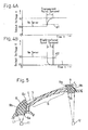
- Fig. 1 illustrates a perspective view of a security sensor according to a first preferred embodiment of the present invention.
- This security sensor 1 includes a generally rectangular box-like carrier body A made up of a generally rectangular base 2 adapted to be fitted to a support surface such as, for example, a ceiling or a wall, and a cap-like cover casing 3 fitted to the base 2 for covering a front surface region of the base 2, and a pyroelectric element 4 which is a passive-type far infrared sensing element and which is accommodated within the carrier body A.
- the casing 3 is detachably secured to the base 2 by means of a plurality of fitting screws (not shown).
- the casing 3 made up of top and bottom walls, side walls and a front wall has a generally rectangular opening in which a lens 5 serving as an incident side enclosure is fitted.
- This lens 5 concurrently serves as a protective covering for protecting the pyroelectric element 4 and is made of a synthetic resin such as, for example, polyethylene of a kind capable of transmitting far infrared rays of light therethrough.
- the lens 5 has an inner surface formed with a Fresnel lens section 6, which section 6 defines a plurality of detection areas B for the pyroelectric element 4.
- a projector-side guide element or a first light guide element 8 and a receiver-side guide element or a second light guide element 9 are mounted on the front wall of the casing 3 so as to cover lower and upper ends of the lens 5, respectively, and as to be held in face-to-face relation with each other across the lens 5.
- the light guide elements 8 and 9 are positioned outside the detection areas B, that is, at respective locations outside an area of incidence of far infrared light on the pyroelectric element 4 shown in Fig. 2 .
- a printed circuit board 10 fitted to the base 2 and positioned within the carrier body A has mounted thereon the pyroelectric element 4, a light projecting element 11 for generating a near infrared light, which is a disturbance detecting light beam L1, so as to be projected towards an incident surface (one of light transmitting surfaces) 8a of the projector-side light guide member 8 and a light receiving element 12 for receiving the disturbance detecting beam L1, which has emerged outwardly from a light exit surface (one of the light transmitting surfaces) 8c of the projector-side light guide member 8 that is exposed to the outside, through the receiver-side light guide member 9.
- the pyroelectric element 4, the light projecting element 11 and the light receiving element 12 are supported on and by the base 2 and are covered by the casing 3 and the lens 5 so as to be accommodated within the carrier body A.
- the projector-side and receiver-side light guide members 8 and 9 are operable to guide the disturbance detecting beam L1 from the light projecting element 11 towards the light receiving element 12 and cooperate with each other to define an optical path L for the disturbance detecting beam L1 that extends along an outer surface of the lens 5.
- the light exit surface 8c of the projector-side light guide member 8 and the light incident surface (one of the light transmitting surfaces) 9a of the receiver-side light guide member 9 that is exposed to the outside and confronts with the light exit surface 8c are ground, that is, formed with fine surface irregularities generally similar to those found on a ground glass.
- the pyroelectric element 4 when detecting through the lens 5 far infrared rays of light emitted from a human body within the detection areas B detects that the human body has intruded the detection areas B.
- the light projecting element 11 when driven by a drive circuit 13 shown in Fig. 3 emits the disturbance detecting beam L1 towards the light incident surface 8a of the projector-side light guide member 8.
- the disturbance detecting beam L1 entering the projector-side light guide member 8 travels in part towards a light reflecting surface 8b of the projector-side light guide member 8, which is exposed to the outside of the projector-side light guide member 8, and in part towards the light exit surface 8c thereof without being reflected by the light reflecting surface 8b.
- That portion of the disturbance detecting beam L1 reaching the light reflecting surface 8c is in part reflected thereby so as to travel towards the light exit surface 8c and in part transmitted through the light reflecting surface 8b to the outside of the projector-side light guide element 8.
- the light emerging outwardly from the light exit surface 8c of the projector-side light guide member 8 is in turn scattered outwardly as shown by the single-dotted chain line and a portion thereof subsequently enters the receiver-side light guide member 9 through the light incident surface 9a.
- the light incident on the light incident surface 9a is scattered and a portion thereof is then reflected by a light reflecting surface (a portion of an outer surface) 9b of the receiver-side light guide member 9 that is exposed to the outside and is defined by an inclined surface confronting the light incident surface 9a of the receiver-side light guide member 9, so that the reflected incident light can be received by the light receiving element 12 through the light exit surface (one of the light transmitting surfaces) 9c of the receiver-side light guide member 9.
- the amount of the light so received by the light receiving element 12 in this way represents a reference incident light amount that is normal in the absence of any obstacle applied to an outer surface of the lens 5. Consequently, an output voltage V from an incident light amount detecting circuit 14 at this time represents a value V0 of a substantially low level as shown in Fig. 4A .
- the obstacle such as, for example, a transparent paint of a kind capable of intercepting far infrared rays of light, but allowing light ranging from a near infrared wavelength region to a visible wavelength region to pass therethrough is applied to the outer surface of the lens 5 shown in Fig. 3 , the obstacle so applied deposits on the light exit surface 8c of the projector-side light guide member 8 and the light incident surface 9a of the receiver-side light guide member 9 to fill up surface irregularities to thereby render the light exit surface 8c and the light incident surface 9a to be flat.
- the obstacle such as, for example, a transparent paint of a kind capable of intercepting far infrared rays of light, but allowing light ranging from a near infrared wavelength region to a visible wavelength region to pass therethrough
- the obstacle such as, for example, a black-colored paint of a kind capable of intercepting not only far infrared rays of light, but also light ranging from a near infrared wavelength region to a visible wavelength region to pass therethrough is so applied to the outer surface of the lens 5 as to deposit on at least one of the light reflecting surface (a portion of the outer surface) 8b and the light exit surface 8c of the projector-side light guide member 8, the disturbance detecting beam L1 may be absorbed by such obstacle and, therefore, the amount of the disturbance detecting beam L1 emerging outwardly from the light exit surface 8c of the projector-side light guide member 8 decreases.
- the obstacle such as, for example, a black-colored paint of a kind capable of intercepting not only far infrared rays of light, but also light ranging from a near infrared wavelength region to a visible wavelength region to pass therethrough
- the output voltage V from the incident light amount detecting circuit 14 for detecting the amount of the light received by the light receiving element 12 decreases down to a low level of V2 which is lower than the value V0 as shown in Fig. 4B .
- a detecting circuit 15 shown in Fig. 3 includes first and second comparators 16 and 17 and a warning circuit 18.
- An output voltage V from the incident light amount detecting circuit 14 is supplied to the first and second comparators 16 and 17 so that the output voltage V can be compared by the first comparator 16 with a first threshold value d1 and also by the second comparator 17 with a second threshold value d2.
- the first threshold value d1 for the first comparator 16 is chosen to be a value that is about 1.1 times the low level voltage V0 outputted from the incident light amount detecting circuit 14 when no obstacle is applied
- the second threshold value d2 for the second comparator 17 is chosen to be a value that is about 0.9 times the low level voltage V0 when no obstacle is applied.
- the first or second comparator 16 or 17 comparing the input voltage V with the first or second threshold value d1 or d2 outputs a disturbance detection signal to the warning circuit 18 when the input voltage V is higher than the first threshold value d1 or lower than the second threshold value d2.
- the warning circuit 18 then operates in response to the disturbance detection signal from either the first comparator 16 or the second comparator 17 to provide a control room (not shown) with a warning signal. In this way, the presence of the obstacle such as the transparent or black-colored paint applied externally to the outer surface of the lens 5 can be detected.
- the respective positions of the light projecting element 11 and the light receiving element 12 can be chosen to be at a position distant from the lens 5 as desired and, therefore, in the illustrated embodiment, the light projecting element 11 and the light receiving elements 12 are positioned on the printed circuit board 10 readily available for the support thereof. Also, since the amount of light received by the light receiving element 12 does not substantially change even when a small object such as, for example, an insect temporarily deposits on the outer surface of the lens 5, the security sensor embodying the present invention will not result in an erroneous operation with the small object detected as an obstacle.
- Fig. 5 illustrates a fragmentary sectional view, on an enlarged scale, of a portion of the security sensor according to an example.
- component parts that are similar to those employed in Fig. 3 are designated by like reference numerals.
- each of the light exit surface 8c of the projector-side light guide member 8 and the light incident surface 9a of the receiver-side light guide member 9 is, in the form of a flat smooth surface whereas the light reflecting surface 9b of the receiver-side light guide member 9 is ground, that is, formed with fine surface irregularities generally similar to those found on a ground glass.
- the amount of the disturbance detecting beam L1 emerging outwardly from the light exit surface 8c of the projector-side light guide member 8 and subsequently entering the receiver-side light guide member 9 is larger than that in the previously described first embodiment.
- the disturbance detecting beam L1 entering the receiver-side light guide member 9 is diffused as it is reflected by the light reflecting surface 9b of the receiver-side light guide member 9, the amount of the disturbance detecting beam L1 received by the light receiving element 12 decreases down to a value about equal to that in the previously described first embodiment.
- the surface irregularities of the light reflecting surface 9b are filled up by the transparent paint to represent a flat smooth surface and, as a result thereof, the amount of the light reflected by the light reflecting surface 9b increases, resulting in increase of the amount of the light received by the light receiving element 12.
- the amount of the light received by the light receiving element 12 decreases as is the case with that described in connection with the first embodiment and, therefore, the presence of the obstacle can be detected in the manner described hereinbefore.
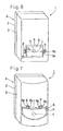
- Fig. 6 illustrates a perspective view of the security sensor according to a second preferred embodiment of the present invention, wherein component parts that are similar to those shown in Fig. 1 are designated by like reference numerals.
- the security sensor according to this second embodiment is of a structure wherein the projector-side light guide member 8 and the receiver-side light guide member 9 are mounted on the cap-like casing 3 at respective locations adjacent opposite sides of the lens 5, i.e., left and right sides of the lens 5 as viewed therein.
- the lens 5 employed in the practice of the third embodiment is in the form of a generally rectangular flat lens.
- the optical path L for the travel of the disturbance detecting beam L1 is defined along the outer surface of the lens 5 so as to extend between the projector-side and receiver-side light guide members 8 and 9.
- One or more surfaces of light exit surface 8c of the projector-side light guide member 8 and the light incident surface 8a of the receiver-side light guide member 9 is ground to provide surface irregularities similar to those found in a ground glass.
- the security sensor 1 according to the second embodiment can function in a manner similar to that according to any one of the first and second embodiments to similarly perform the disturbance detecting capability.
- Fig. 7 illustrates a perspective view of the security sensor according to a third preferred embodiment of the present invention, wherein component parts that are similar to those shown in Fig. 1 are designated by like reference numerals.
- the security sensor according to this third embodiment is of a structure wherein the projector-side light guide member 8 and the receiver-side light guide member 9 are mounted on the cap-like casing 3 at respective locations adjacent one side of the lens 5, for example, an upper side of the lens 5 as viewed therein.
- the lens 5 employed in the practice of the fourth embodiment is in the form of a convex plate having a relatively small radius of curvature.
- the optical path L for the travel of the disturbance detecting beam L1 is defined along the outer surface of the lens 5 so as to extend between the projector-side and receiver-side light guide members 8 and 9.
- the light exit surface 8c of the projector-side light guide member 8 and the light incident surface 9a of the receiver-side light guide member 9 are spaced a small distance from each other so as to confront each other so that the optical path L for the disturbance detecting beam L1 that extends between the light exit surface 8c and the light incident surface 9a will not be obstructed by a convex surface of the lens 5.
- the security sensor 1 can function in a manner similar to that according to any one of the first and second embodiments to similarly perform the disturbance detecting capability.
- Figs. 8 and 9 illustrate the security sensor according a fourth embodiment of the present invention, wherein Fig. 8 represents the cross-sectional view taken along the line VIII-VIII in Fig. 9 and Fig. 9 represents the cross-sectional view taken along the line IX-IX in Fig. 8 .
- Component parts which are shown in Figs. 8 and 9 , but are similar to those shown in Figs. 1 to 3 are identified by like reference numerals used in Figs. 1 to 3 .
- the security sensor 1 similarly includes a box-like carrier body A made up of a generally rectangular base 2 adapted to be fitted to a support surface such as, for example, a ceiling S.
- a printed circuit board 10 is fitted to the base 2 and includes a pair of support members 20 and 20 mounted thereon.
- a carrier substrate 21 is adjustably supported by the support members 20 and 20 for rotation about an axis connecting between the support members 20 and 20 and has a pyroelectric element 4 and a polygon mirror 22 mounted on the carrier substrate 21 so as to define a plurality of detection areas B.
- a semispherical cover (incident side enclosure) 24 made of an opaque synthetic resin is capped onto the base 2 so as to enclose incident surface areas of the pyroelectric element 4 and polygon mirror 22.
- projector-side and receiver-side light guide members 8 and 9 are mounted on the semispherical cover 24 and are positioned outside a portion of the cover 24 where the detection areas B extend, that is, outside an light incident area through which the near infrared light is incident on the pyroelectric element 4, so that the light exit surface 8c of the projector-side light guide member 8 can assume a face-to-face relation with the light incident surface 9a of the receiver-side light guide member 9 with an optical L defined therebetween for the disturbance detecting light L1.
- the semispherical cover 24 employed in the embodiment shown in Figs. 8 and 9 serves merely to protect the sensor carrier body A and has no lens capability that defines the detection areas.
- the light projecting and receiving elements 11 and 12 are fixedly mounted on the printed circuit board 10.
- the pyroelectric element 4 and the light projecting and receiving elements 11 and 12 are supported by the base 2 forming a part of the sensor carrier body A and are encased by the semispherical cover 24 fitted to the base 2.
- the light projecting element 11 is electrically connected with the drive circuit 13 shown in Fig. 3
- the light receiving element 12 is electrically connected with the incident light amount detecting circuit 14 and the detecting circuit 15 both also shown in Fig. 3 .
- the light exit surface 8c of the projector-side light guide member 8 that is ground to have the surface irregularities and the light incident surface 9a of the receiver-side light guide member 9 that is also ground to have the surface irregularities cooperate to define the optical path L extending therebetween for the disturbance detecting beam L1.
- This optical path L extends straight between the light exit surface 8c of the projector-side light guide member 8 and the light incident surface 9a of the receiver-side light guide member 9 over the curved outer surface of the cover 24 with the light guide members 8 and 9 protruding outwardly from the cover 24.
- the amount of the light received by the light receiving element 12 increases to a value higher or decreases a value lower than that exhibited when no obstacle is applied and, therefore, the presence of the obstacle can be detected by the detecting circuit 15.
- the obstacle with which the security sensor embodying the present invention can work may include, other than the transparent paint referred to in the foregoing description, an adhesive tape of transparent plastics or cellophane, a gel or creamy adhesive material or a sealant.
- an adhesive tape of transparent plastics or cellophane a gel or creamy adhesive material or a sealant.
- the obstacle is a liquid medium such as, for example, water or oil
- deposit of such an obstacle renders the surface irregularities of the light reflecting surface, the light exit surface or the light incident surface to represent a substantially flat surface before it dries up and, therefore, the amount of the light received by the light receiving element 12 varies so that the presence of the obstacle can be detected by the detecting circuit 15.
- the surface where the surface irregularities are formed may be a part of or the entirety of at least one of the surfaces exposed to the outside, the light exit surface 8c (both of the projector-side light guide member 8), or the light incident surface 9a (both of the receiver-side light guide member 9). It is also to be noted that the projector-side light guide member 8 or the receiver-side light guide member 9 may have a portion thereof positioned within the area of incidence of the near infrared light on the pyroelectric element 4.
Abstract
Description
- The present invention generally relates to a security sensor of a type utilizing a passive-type infrared sensor element and, more particularly, to the security sensor of a type having a disturbance detecting capability for detecting the presence or absence of an obstacle such as, for example, a transparent paint applied to the sensor casing to disable the security sensor.
- An intruder detecting system utilizing the security sensor of the type referred to above is so designed and so configured as to detect an intruder within a detection area or an area of surveillance in reference to the difference between the temperature of a human body and the ambient temperature when the passive-type infrared sensor element receives far infrared rays of light emitted from the human body within the detection area,
- It has often been experienced that the intruder detecting system is tampered with an obstacle such as, for example, a transparent paint of a kind capable of transmitting therethrough rays of light ranging from a visible wavelength region to a near infrared wavelength region, but intercepting far infrared rays of light, so that the intruder detecting system may be fooled enough to allow an intruder to trespass on the detection area monitored by the passive-type infrared sensor element. For example, while the intruder detecting system is held inoperative because the detection area is crowded with people moving in and out of the detection area, a potential intruder may enter the detection area and then apply or otherwise spray the transparent paint of the kind referred to above to a light receiving enclosure or an incident side enclosure such as, for example, a sensor lens or cover through which the far infrared rays of light enter, so that the potential intruder can enter again the detection area later while the intruder detecting system is switched in operation with the detection area no longer crowded with people.
- In view of the above, the security sensor equipped with a disturbance detector for detecting the presence or absence of the obstacle has been well known in the art and is disclosed in, for example, the Japanese Laid-open Patent Publication No.
2-287278 - It has, however, been found that with the disturbance detector used in the prior art security sensor, detection of the increment of the light reflected from the obstacle is difficult to achieve where the amount of the obstacle detecting light reflected from the obstacle is insufficiently small relative to the standard amount of the light incident on the light receiving element because the obstacle detecting light reflected from the inner surface of the lens may travel astray.
- In particular, in the event that the paint of a kind capable of intercepting passage of far infrared rays of light therethrough is applied or sprayed to a front surface of the lens, the amount of light reflected from the paint decreases so extremely that the disturbance detector may fail to detect it. Moreover, since the transparent paint when applied to the front surface of the lens is virtually discernable with eyes, the presence or absence of the obstacle on the lens is not easy to detect with eyes.
- In order to detect the presence of the obstacle such as the transparent paint of the kind discussed above, attempts have hitherto been made to capture an instantaneous change of the amount of the obstacle detecting light when the obstacle is applied (i.e., to detect the act of applying the obstacle) or to employ an increased emitting and receiving power of the disturbance detector. However, the former does not only require the disturbance detector to be activated at all times, but also is susceptible to an erroneous detection resulting from an erroneous operation of the disturbance detector. On the other hand, the latter may often result in an erroneous detection even when small insects traverse.
-
EP-A-0817148 discloses a security sensor in which infra-red radiation passes through a window in a carrier body of the sensor and is detected by an infra-red sensor element in the body. To prevent the sensor being compromised by the application of a film to the window, two light guide members are mounted on opposite sides of the window to conduct light from a light source to a light receiver via the surface of the window. A detecting circuit can then detect the presence of the film by changes in the intensity of the light received by the light receiver. - According to the present invention there is provided a security sensor according to
claim 1. - According to the present invention, when the transparent paint is applied to the outer surface of the incident side enclosure and the applied transparent paint deposits in at least some of the surface irregularities, such irregularities are filled up to define a substantially flat surface and, therefore, the amount of light incident on the light receiving element increases. In the event that a black-colored paint is applied to the outer surface of the incident side enclosure and the applied black-colored paint deposits on the light transmitting of the first or second light guide member, the amount of light incident on the light receiving element decreases. Accordingly, the presence of the obstacle such as the transparent paint or the black-colored paint intercepting the far infrared light, but transmitting the disturbance detecting light can be assuredly detected. Also, even though a small obstacle such as a fly or an insect perches temporarily on the outer surface of the incident side enclosure, and since the amount of the light reflected from such small obstacle is small, there is no possibility of the security sensor functioning erroneously.
- In a preferred embodiment of the present invention, the first light guide member has a first light incident surface, a first light exit surface and a first light reflecting surface defined therein and is operable to guide the beam from the first light incident surface towards the first light exit surface through the first light reflecting surface, and the second light guide ember has a second light incident surface, a second light exit surface and a second light reflecting surface defined therein and is operable to guide the beam from the second light incident surface towards the second light exit surface through the second light reflecting surface. The surface irregularities are preferably formed on at least one of the first light exit surface, or, the second light incident surface.
- Also, in a preferred embodiment of the present invention, the first and second light guide members are mounted on the carrier body at respective locations outside an area of incidence of infrared light on the infrared sensor element. This is particularly advantageous in that the use of the first and second light guide members will not lower the detecting capability of the security sensor.
- Preferably the infrared sensor element, the light projecting element and the light receiving element may be mounted on a common circuit board. This is particularly advantageous in that since only one circuit board is sufficient, the structure of the security sensor can be simplified.
- Also preferably, the carrier body comprises a support base for supporting the infrared sensor element, the light projecting element and the light receiving element, a casing and a lens which defines the incident side enclosure and fitted to the casing with the infrared sensor element, the light projecting element and the light receiving element being covered by the casing and the lens. The first and second light guide members may then be positioned on the casing at respective locations adjacent the lens. This arrangement is directed to the security sensor of a type wherein the lens exposed to the outside is used to cover frontward of the detecting elements.
- Again, the carrier body may comprise a support base for supporting the infrared sensor element, the light projecting element and the light receiving element, and a cover which defines the incident side enclosure and fitted to the support base so as to enclose the infrared sensor element, the light projecting element and the light receiving element, and wherein the first and second light guide members are positioned on the cover at respective locations spaced a distance from each other. This arrangement is directed to the security sensor of a type wherein the cover is used to enclose the circuit boards including the infrared sensor element.
- In any event, the present invention will become more clearly understood from the following description of preferred embodiments thereof, when taken in conjunction with the accompanying drawings. However, the embodiments and the drawings are given only for the purpose of illustration and explanation, and are not to be taken as limiting the scope of the present invention in any way whatsoever, which scope is to be determined by the appended claims. In the accompanying drawings, like reference numerals are used to denote like parts throughout the several views, and:
-
Fig. 1 is a perspective view of a security sensor having a disturbance detecting capability according to a first preferred embodiment of the present invention; -
Fig. 2 is a cross-sectional view taken along the line II-II inFig. 1 ; -
Fig. 3 is a fragmentary sectional view, shown together with a block diagram of a disturbance detecting circuit, showing the manner of propagation of light within first and second light guide members employed in the first preferred embodiment of the present invention; -
Fig. 4A is a chart showing an output voltage characteristic of an incident light amount detecting circuit used in the first preferred embodiment of the present invention, when a transport obstacle is applied to a lens used in the security sensor; -
Fig. 4B is a chart showing an output voltage characteristic of an incident light amount detecting circuit used in the first preferred embodiment of the present invention, when a black-colored obstacle is applied to a lens used in the security sensor; -
Fig. 5 is a fragmentary sectional view, on an enlarged scale, of a portion of the security sensor according to an example, which is not an embodiment of the invention; and -
Fig. 6 is a perspective view of the security sensor having a disturbance detecting capability according to a second preferred embodiment of the present invention; -
Fig. 7 is a perspective view of the security sensor having a disturbance detecting capability according to a third preferred embodiment of the present invention; -
Fig. 8 is a sectional view of the security sensor having a disturbance detecting capability according to a fourth preferred embodiment of the present invention; and -
Fig. 9 is a cross-sectional view taken along the line IX-IX inFig. 8 . - Hereinafter, preferred embodiments of the present invention will be described with reference to the accompanying drawings.
-
Fig. 1 illustrates a perspective view of a security sensor according to a first preferred embodiment of the present invention. Thissecurity sensor 1 includes a generally rectangular box-like carrier body A made up of a generallyrectangular base 2 adapted to be fitted to a support surface such as, for example, a ceiling or a wall, and a cap-like cover casing 3 fitted to thebase 2 for covering a front surface region of thebase 2, and apyroelectric element 4 which is a passive-type far infrared sensing element and which is accommodated within the carrier body A. Thecasing 3 is detachably secured to thebase 2 by means of a plurality of fitting screws (not shown). - As shown in
Fig. 2 , thecasing 3 made up of top and bottom walls, side walls and a front wall has a generally rectangular opening in which alens 5 serving as an incident side enclosure is fitted. Thislens 5 concurrently serves as a protective covering for protecting thepyroelectric element 4 and is made of a synthetic resin such as, for example, polyethylene of a kind capable of transmitting far infrared rays of light therethrough. Thelens 5 has an inner surface formed with a Fresnellens section 6, whichsection 6 defines a plurality of detection areas B for thepyroelectric element 4. A projector-side guide element or a firstlight guide element 8 and a receiver-side guide element or a secondlight guide element 9 are mounted on the front wall of thecasing 3 so as to cover lower and upper ends of thelens 5, respectively, and as to be held in face-to-face relation with each other across thelens 5. Thelight guide elements pyroelectric element 4 shown inFig. 2 . - A printed
circuit board 10 fitted to thebase 2 and positioned within the carrier body A has mounted thereon thepyroelectric element 4, alight projecting element 11 for generating a near infrared light, which is a disturbance detecting light beam L1, so as to be projected towards an incident surface (one of light transmitting surfaces) 8a of the projector-sidelight guide member 8 and alight receiving element 12 for receiving the disturbance detecting beam L1, which has emerged outwardly from a light exit surface (one of the light transmitting surfaces) 8c of the projector-sidelight guide member 8 that is exposed to the outside, through the receiver-sidelight guide member 9. In this way, thepyroelectric element 4, thelight projecting element 11 and thelight receiving element 12 are supported on and by thebase 2 and are covered by thecasing 3 and thelens 5 so as to be accommodated within the carrier body A. The projector-side and receiver-sidelight guide members light projecting element 11 towards thelight receiving element 12 and cooperate with each other to define an optical path L for the disturbance detecting beam L1 that extends along an outer surface of thelens 5. Thelight exit surface 8c of the projector-sidelight guide member 8 and the light incident surface (one of the light transmitting surfaces) 9a of the receiver-sidelight guide member 9 that is exposed to the outside and confronts with thelight exit surface 8c are ground, that is, formed with fine surface irregularities generally similar to those found on a ground glass. - The
pyroelectric element 4 when detecting through thelens 5 far infrared rays of light emitted from a human body within the detection areas B detects that the human body has intruded the detection areas B. Thelight projecting element 11 when driven by adrive circuit 13 shown inFig. 3 emits the disturbance detecting beam L1 towards thelight incident surface 8a of the projector-sidelight guide member 8. The disturbance detecting beam L1 entering the projector-sidelight guide member 8 travels in part towards alight reflecting surface 8b of the projector-sidelight guide member 8, which is exposed to the outside of the projector-sidelight guide member 8, and in part towards thelight exit surface 8c thereof without being reflected by thelight reflecting surface 8b. That portion of the disturbance detecting beam L1 reaching thelight reflecting surface 8c is in part reflected thereby so as to travel towards thelight exit surface 8c and in part transmitted through thelight reflecting surface 8b to the outside of the projector-sidelight guide element 8. In any event, the light emerging outwardly from thelight exit surface 8c of the projector-sidelight guide member 8 is in turn scattered outwardly as shown by the single-dotted chain line and a portion thereof subsequently enters the receiver-sidelight guide member 9 through thelight incident surface 9a. The light incident on thelight incident surface 9a is scattered and a portion thereof is then reflected by a light reflecting surface (a portion of an outer surface) 9b of the receiver-sidelight guide member 9 that is exposed to the outside and is defined by an inclined surface confronting thelight incident surface 9a of the receiver-sidelight guide member 9, so that the reflected incident light can be received by thelight receiving element 12 through the light exit surface (one of the light transmitting surfaces) 9c of the receiver-sidelight guide member 9. The amount of the light so received by thelight receiving element 12 in this way represents a reference incident light amount that is normal in the absence of any obstacle applied to an outer surface of thelens 5. Consequently, an output voltage V from an incident lightamount detecting circuit 14 at this time represents a value V0 of a substantially low level as shown inFig. 4A . - However, in the event that the obstacle such as, for example, a transparent paint of a kind capable of intercepting far infrared rays of light, but allowing light ranging from a near infrared wavelength region to a visible wavelength region to pass therethrough is applied to the outer surface of the
lens 5 shown inFig. 3 , the obstacle so applied deposits on thelight exit surface 8c of the projector-sidelight guide member 8 and thelight incident surface 9a of the receiver-sidelight guide member 9 to fill up surface irregularities to thereby render thelight exit surface 8c and thelight incident surface 9a to be flat. Therefore, scattering of the disturbance detecting beam L1 emerging outwardly from thelight exit surface 8c of the projector-sidelight guide member 8 is reduced, resulting in increase of the amount of the disturbance detecting beam L1 incident on thelight incident surface 9a of the receiver-sidelight guide member 9, and also the scattering of the light at thelight incident surface 9a is reduced. Consequently, the amount of the disturbance detecting beam L1 incident on thelight receiving element 12 increases whereby the output voltage V from the incident lightamount detecting circuit 14 for detecting the amount of the light received by thelight receiving element 12 increases to a high level of V1 which is higher than the value V0 as shown inFig. 4A . - On the other hand, in the event that the obstacle such as, for example, a black-colored paint of a kind capable of intercepting not only far infrared rays of light, but also light ranging from a near infrared wavelength region to a visible wavelength region to pass therethrough is so applied to the outer surface of the
lens 5 as to deposit on at least one of the light reflecting surface (a portion of the outer surface) 8b and thelight exit surface 8c of the projector-sidelight guide member 8, the disturbance detecting beam L1 may be absorbed by such obstacle and, therefore, the amount of the disturbance detecting beam L1 emerging outwardly from thelight exit surface 8c of the projector-sidelight guide member 8 decreases. Even when the black-colored paint deposits on at least one of thelight incident surface 9a and thelight reflecting surface 9b of the receiver-sidelight guide member 9, the amount of the light received by thelight guide element 12 through the receiver-sidelight guide member 9 similarly decreases. Consequently, the output voltage V from the incident lightamount detecting circuit 14 for detecting the amount of the light received by thelight receiving element 12 decreases down to a low level of V2 which is lower than the value V0 as shown inFig. 4B . - A detecting
circuit 15 shown inFig. 3 includes first andsecond comparators 16 and 17 and awarning circuit 18. An output voltage V from the incident lightamount detecting circuit 14 is supplied to the first andsecond comparators 16 and 17 so that the output voltage V can be compared by the first comparator 16 with a first threshold value d1 and also by thesecond comparator 17 with a second threshold value d2. By way of example, the first threshold value d1 for the first comparator 16 is chosen to be a value that is about 1.1 times the low level voltage V0 outputted from the incident lightamount detecting circuit 14 when no obstacle is applied, whereas the second threshold value d2 for thesecond comparator 17 is chosen to be a value that is about 0.9 times the low level voltage V0 when no obstacle is applied. - Depending on the type of the obstacle, for example, the transparent paint or the black-colored paint, applied to the outer surface of the
lens 5, the first orsecond comparator 16 or 17 comparing the input voltage V with the first or second threshold value d1 or d2 outputs a disturbance detection signal to thewarning circuit 18 when the input voltage V is higher than the first threshold value d1 or lower than the second threshold value d2. Thewarning circuit 18 then operates in response to the disturbance detection signal from either the first comparator 16 or thesecond comparator 17 to provide a control room (not shown) with a warning signal. In this way, the presence of the obstacle such as the transparent or black-colored paint applied externally to the outer surface of thelens 5 can be detected. - Also, since the disturbance detecting beam L1 guided through the projector-side
light guide member 8 and then through the receiver-sidelight guide member 9 is received by thelight receiving element 12, the respective positions of thelight projecting element 11 and thelight receiving element 12 can be chosen to be at a position distant from thelens 5 as desired and, therefore, in the illustrated embodiment, thelight projecting element 11 and thelight receiving elements 12 are positioned on the printedcircuit board 10 readily available for the support thereof. Also, since the amount of light received by thelight receiving element 12 does not substantially change even when a small object such as, for example, an insect temporarily deposits on the outer surface of thelens 5, the security sensor embodying the present invention will not result in an erroneous operation with the small object detected as an obstacle. -
Fig. 5 illustrates a fragmentary sectional view, on an enlarged scale, of a portion of the security sensor according to an example. In this figure, component parts that are similar to those employed inFig. 3 are designated by like reference numerals. - The security sensor shown in
Fig. 5 is featured in that each of thelight exit surface 8c of the projector-sidelight guide member 8 and thelight incident surface 9a of the receiver-sidelight guide member 9 is, in the form of a flat smooth surface whereas thelight reflecting surface 9b of the receiver-sidelight guide member 9 is ground, that is, formed with fine surface irregularities generally similar to those found on a ground glass. - According to this example, the amount of the disturbance detecting beam L1 emerging outwardly from the
light exit surface 8c of the projector-sidelight guide member 8 and subsequently entering the receiver-sidelight guide member 9 is larger than that in the previously described first embodiment. However, since the disturbance detecting beam L1 entering the receiver-sidelight guide member 9 is diffused as it is reflected by thelight reflecting surface 9b of the receiver-sidelight guide member 9, the amount of the disturbance detecting beam L1 received by thelight receiving element 12 decreases down to a value about equal to that in the previously described first embodiment. In the event that the transparent paint is applied and deposits on thelight reflecting surface 9b of the receiver-sidelight guide member 9, the surface irregularities of thelight reflecting surface 9b are filled up by the transparent paint to represent a flat smooth surface and, as a result thereof, the amount of the light reflected by thelight reflecting surface 9b increases, resulting in increase of the amount of the light received by thelight receiving element 12. Also, in the event of the black-colored paint applied, the amount of the light received by thelight receiving element 12 decreases as is the case with that described in connection with the first embodiment and, therefore, the presence of the obstacle can be detected in the manner described hereinbefore. -
Fig. 6 illustrates a perspective view of the security sensor according to a second preferred embodiment of the present invention, wherein component parts that are similar to those shown inFig. 1 are designated by like reference numerals. The security sensor according to this second embodiment is of a structure wherein the projector-sidelight guide member 8 and the receiver-sidelight guide member 9 are mounted on the cap-like casing 3 at respective locations adjacent opposite sides of thelens 5, i.e., left and right sides of thelens 5 as viewed therein. Thelens 5 employed in the practice of the third embodiment is in the form of a generally rectangular flat lens. The optical path L for the travel of the disturbance detecting beam L1 is defined along the outer surface of thelens 5 so as to extend between the projector-side and receiver-sidelight guide members light exit surface 8c of the projector-sidelight guide member 8 and thelight incident surface 8a of the receiver-sidelight guide member 9 is ground to provide surface irregularities similar to those found in a ground glass. Thesecurity sensor 1 according to the second embodiment can function in a manner similar to that according to any one of the first and second embodiments to similarly perform the disturbance detecting capability. -
Fig. 7 illustrates a perspective view of the security sensor according to a third preferred embodiment of the present invention, wherein component parts that are similar to those shown inFig. 1 are designated by like reference numerals. The security sensor according to this third embodiment is of a structure wherein the projector-sidelight guide member 8 and the receiver-sidelight guide member 9 are mounted on the cap-like casing 3 at respective locations adjacent one side of thelens 5, for example, an upper side of thelens 5 as viewed therein. Thelens 5 employed in the practice of the fourth embodiment is in the form of a convex plate having a relatively small radius of curvature. The optical path L for the travel of the disturbance detecting beam L1 is defined along the outer surface of thelens 5 so as to extend between the projector-side and receiver-sidelight guide members light exit surface 8c of the projector-sidelight guide member 8 and thelight incident surface 9a of the receiver-sidelight guide member 9 are spaced a small distance from each other so as to confront each other so that the optical path L for the disturbance detecting beam L1 that extends between thelight exit surface 8c and thelight incident surface 9a will not be obstructed by a convex surface of thelens 5. - Even in this third embodiment of the present invention, as one or more surfaces and
light exit surface 8c of the projector-sidelight guide member 8 and thelight incident surface 8a of the receiver-sidelight guide member 9 is ground to provide surface irregularities similar to those found in a ground glass, thesecurity sensor 1 according to the third embodiment can function in a manner similar to that according to any one of the first and second embodiments to similarly perform the disturbance detecting capability. -
Figs. 8 and 9 illustrate the security sensor according a fourth embodiment of the present invention, whereinFig. 8 represents the cross-sectional view taken along the line VIII-VIII inFig. 9 and Fig. 9 represents the cross-sectional view taken along the line IX-IX inFig. 8 . Component parts which are shown inFigs. 8 and 9 , but are similar to those shown inFigs. 1 to 3 are identified by like reference numerals used inFigs. 1 to 3 . - The
security sensor 1 similarly includes a box-like carrier body A made up of a generallyrectangular base 2 adapted to be fitted to a support surface such as, for example, a ceiling S. A printedcircuit board 10 is fitted to thebase 2 and includes a pair ofsupport members carrier substrate 21 is adjustably supported by thesupport members support members pyroelectric element 4 and apolygon mirror 22 mounted on thecarrier substrate 21 so as to define a plurality of detection areas B. A semispherical cover (incident side enclosure) 24 made of an opaque synthetic resin is capped onto thebase 2 so as to enclose incident surface areas of thepyroelectric element 4 andpolygon mirror 22. As shown inFig. 9 , projector-side and receiver-sidelight guide members semispherical cover 24 and are positioned outside a portion of thecover 24 where the detection areas B extend, that is, outside an light incident area through which the near infrared light is incident on thepyroelectric element 4, so that thelight exit surface 8c of the projector-sidelight guide member 8 can assume a face-to-face relation with thelight incident surface 9a of the receiver-sidelight guide member 9 with an optical L defined therebetween for the disturbance detecting light L1. Thesemispherical cover 24 employed in the embodiment shown inFigs. 8 and 9 serves merely to protect the sensor carrier body A and has no lens capability that defines the detection areas. The light projecting and receivingelements circuit board 10. Thus, thepyroelectric element 4 and the light projecting and receivingelements base 2 forming a part of the sensor carrier body A and are encased by thesemispherical cover 24 fitted to thebase 2. Thelight projecting element 11 is electrically connected with thedrive circuit 13 shown inFig. 3 whereas thelight receiving element 12 is electrically connected with the incident lightamount detecting circuit 14 and the detectingcircuit 15 both also shown inFig. 3 . - In the
security sensor 1 according to the embodiment shown inFigs. 8 and 9 , thelight exit surface 8c of the projector-sidelight guide member 8 that is ground to have the surface irregularities and thelight incident surface 9a of the receiver-sidelight guide member 9 that is also ground to have the surface irregularities cooperate to define the optical path L extending therebetween for the disturbance detecting beam L1. This optical path L extends straight between thelight exit surface 8c of the projector-sidelight guide member 8 and thelight incident surface 9a of the receiver-sidelight guide member 9 over the curved outer surface of thecover 24 with thelight guide members cover 24. - Accordingly, as is the case with the previously described first embodiment of the present invention, in the event that the obstacle, such as the transparent paint or the black-colored paint, deposits on one or both of the
light exit surface 8c and thelight incident surface 9a, the amount of the light received by thelight receiving element 12 increases to a value higher or decreases a value lower than that exhibited when no obstacle is applied and, therefore, the presence of the obstacle can be detected by the detectingcircuit 15. - The obstacle with which the security sensor embodying the present invention can work may include, other than the transparent paint referred to in the foregoing description, an adhesive tape of transparent plastics or cellophane, a gel or creamy adhesive material or a sealant. Where the obstacle of this kind is applied to the outer surface of the
lens 5, the surface irregularities of onelight exit surface 8c of the projector-sidelight guide member 8, or thelight incident surface 9a of the receiver-sidelight guide member 9 are filled up by the obstacle due to its own viscosity and, therefore, the amount of the light received by thelight receiving element 12 varies so that the presence of the obstacle can be detected by the detectingcircuit 15 then detecting such a change in amount of the light received by thelight receiving element 12. Even where the obstacle is a liquid medium such as, for example, water or oil, deposit of such an obstacle renders the surface irregularities of the light reflecting surface, the light exit surface or the light incident surface to represent a substantially flat surface before it dries up and, therefore, the amount of the light received by thelight receiving element 12 varies so that the presence of the obstacle can be detected by the detectingcircuit 15. - It is to be noted that in any one of the foregoing embodiments the surface where the surface irregularities are formed may be a part of or the entirety of at least one of the surfaces exposed to the outside, the
light exit surface 8c (both of the projector-side light guide member 8), or thelight incident surface 9a (both of the receiver-side light guide member 9). It is also to be noted that the projector-sidelight guide member 8 or the receiver-sidelight guide member 9 may have a portion thereof positioned within the area of incidence of the near infrared light on thepyroelectric element 4. - Although the present invention has been fully described in connection with the preferred embodiments thereof with reference to the accompanying drawings which are used only for the purpose of illustration, those skilled in the art will readily conceive numerous changes and modifications within the framework of obviousness upon the reading of the specification herein presented of the present invention. Accordingly, such changes and modifications are, unless they depart from the scope of the present invention as delivered from the claims annexed hereto, to be construed as included therein.
Claims (6)
- A security sensor having a disturbance detecting capability, which comprises:a carrier body (A) having an infrared sensor element (4);an incident side enclosure (3,5) mounted on the carrier body (A), said incident side enclosure (3,5) comprising a lens (5) that defines at least one detection area for the infrared sensor element (4) or a cover that covers an incident surface area of the infrared sensor element (4);a light projecting element (11) for projecting a disturbance detecting beam;a light receiving element (12) for receiving at least a portion of the disturbance detecting beam;first and second light guide members (8,9) operatively associated with the light projecting element (11) and the light receiving element (12), respectively, said first and second light guide members (8,9) being cooperative with each other to define an optical path along and adjacent an outer surface of the incident side enclosure (5) or an outer surface of the carrier body adjacent the incident side enclosure (5) so as to extend between the first and second light guide members (8,9); anda detecting circuit (14) for detecting a presence or absence of an obstacle, based on an amount of light received by the light receiving element (12);wherein surface irregularities are formed on a light transmitting surface (8c,9a), which transmits said disturbance detecting beam, of the first or second light guide member (8,9), and the light transmitting surface (8c,9a) having said surface irregularities is exposed outwardly at the optical path, so as to scatter the disturbance detecting beam
passing therethrough and to reduce scattering of the disturbance detecting beam when transparent paint as the obstacle is deposited on the light transmitting surface (8c,9a), whereby the detecting circuit (14) is arranged to detect the presence or absence of the obstacle when the obstacle is applied to at least said light transmitting surface (8c,9a) having said surface irregularities. - The security sensor as claimed in Claim 1, wherein the first light guide member (8) has a first light incident surface (8a), a first light exit surface (8c) and a first light reflecting surface (8b) defined therein and is operable to guide the beam from the first light incident surface (8a) towards the first light exit surface (8c) through the first light reflecting surface (8b), and the second light guide member (9) has a second light incident surface (9a), a second light exit surface (9c) and a second light reflecting surface (9b) defined therein and is operable to guide the beam from the second light incident surface (9a) towards the second light exit surface (9c) through the second light reflecting surface (9b), and wherein the surface irregularities are formed on at least one of the first light exit surface (8c) and the second light incident surface (9a).
- The security sensor as claimed in Claim 1 or 2, wherein the first and second light guide members (8a) are mounted on the carrier body (A) at respective locations outside an area of incidence of infrared light on the infrared sensor element (4).
- The security sensor as claimed in any one of the preceding claims, wherein the infrared sensor element (4), the light projecting element (11) and the light receiving element (12) are mounted on a common circuit board (10).
- The security sensor as claimed in any one of the preceding claims, wherein the carrier body (A) comprises a support base (2) for supporting the infrared sensor element (4), the light projecting element (11) and the light receiving element (12), a casing (3) and a lens (5) which defines the incident side enclosure and fitted to the casing (3) with the infrared sensor element (4), the light projecting element (11) and the light receiving element (12) being covered by the casing (3) and the lens, and wherein the first and second light guide members (8,9) are positioned on the casing (3) at respective locations adjacent the lens (5).
- The security sensor as claimed in one of Claims 1 to 5, wherein the carrier body comprises a support base (2) for supporting the infrared sensor element (4), the light projecting element (11) and the light receiving element (12), and a cover (3) which defines the incident side enclosure and fitted to the support base so as to enclose the infrared sensor element (4), the light projecting element (11) and the light receiving element (12), and wherein the first and second light guide members (8,9) are positioned on the cover (3) at respective locations spaced a distance from each other.
Priority Applications (1)
| Application Number | Priority Date | Filing Date | Title |
|---|---|---|---|
| DE60113316.1T DE60113316T3 (en) | 2000-02-18 | 2001-02-09 | Security sensor with sabotage detection capability |
Applications Claiming Priority (2)
| Application Number | Priority Date | Filing Date | Title |
|---|---|---|---|
| JP2000040702 | 2000-02-18 | ||
| JP2000040702A JP2001228020A (en) | 2000-02-18 | 2000-02-18 | Crime prevention sensor with obstruction detecting function |
Publications (4)
| Publication Number | Publication Date |
|---|---|
| EP1126430A2 EP1126430A2 (en) | 2001-08-22 |
| EP1126430A3 EP1126430A3 (en) | 2002-08-28 |
| EP1126430B1 EP1126430B1 (en) | 2005-09-14 |
| EP1126430B2 true EP1126430B2 (en) | 2013-12-18 |
Family
ID=18564043
Family Applications (1)
| Application Number | Title | Priority Date | Filing Date |
|---|---|---|---|
| EP01301141.6A Expired - Lifetime EP1126430B2 (en) | 2000-02-18 | 2001-02-09 | Security sensor having disturbance detecting capability |
Country Status (4)
| Country | Link |
|---|---|
| US (1) | US6529129B1 (en) |
| EP (1) | EP1126430B2 (en) |
| JP (1) | JP2001228020A (en) |
| DE (1) | DE60113316T3 (en) |
Families Citing this family (28)
| Publication number | Priority date | Publication date | Assignee | Title |
|---|---|---|---|---|
| JP2001229473A (en) * | 2000-02-18 | 2001-08-24 | Optex Co Ltd | Crime-preventive sensor with disturbance detecting function |
| NL1019039C2 (en) * | 2001-09-26 | 2003-03-27 | Interlogix B V | Surveillance detector. |
| JP3587466B2 (en) * | 2002-10-02 | 2004-11-10 | 三菱電機株式会社 | Vehicle periphery monitoring device |
| MXPA05011033A (en) * | 2003-04-11 | 2006-09-05 | Strattec Security Corp | Ignition apparatus and method. |
| JP4879587B2 (en) * | 2005-01-27 | 2012-02-22 | エフビーオートメ株式会社 | Security alarm device |
| WO2007090458A1 (en) * | 2006-02-06 | 2007-08-16 | Robert Bosch Gmbh | Obstruction detection device |
| ES2405354T3 (en) * | 2006-02-20 | 2013-05-30 | Robert Bosch Gmbh | Obstruction Detection Device |
| US7733226B2 (en) * | 2006-03-16 | 2010-06-08 | Robert Bosch Gmbh | Infrared intrusion detection device |
| US20080083868A1 (en) * | 2006-06-16 | 2008-04-10 | Hong Kong Applied Science And Technology Research Institute Co. Ltd. | Monitoring devices and surveillance devices |
| US7414236B2 (en) * | 2006-06-16 | 2008-08-19 | Hong Kong Applied Science And Technology Research Institute Co., Ltd. | Monitoring devices and intrusion surveillance devices |
| WO2008012805A2 (en) | 2006-07-27 | 2008-01-31 | Visonic Ltd | Passive infrared detectors |
| US8319638B2 (en) * | 2007-11-14 | 2012-11-27 | Honeywell International Inc. | Motion detector for detecting tampering and method for detecting tampering |
| US7852210B2 (en) * | 2007-12-31 | 2010-12-14 | Honeywell International Inc. | Motion detector for detecting tampering and method for detecting tampering |
| EP2128832A1 (en) * | 2008-05-30 | 2009-12-02 | Robert Bosch GmbH | Anti-masking system and method for motion detectors |
| US7788770B2 (en) * | 2008-06-06 | 2010-09-07 | Audiovox Corporation | Hinge for a mobile video system |
| US20110173890A1 (en) * | 2010-01-20 | 2011-07-21 | Gantner Mark A | Garage Door Sensor Protector |
| EP2498232A1 (en) * | 2011-03-10 | 2012-09-12 | Siemens Aktiengesellschaft | Detector |
| US9123222B2 (en) * | 2012-03-15 | 2015-09-01 | Ninve Jr. Inc. | Apparatus and method for detecting tampering with an infra-red motion sensor |
| CN103809211B (en) * | 2014-02-18 | 2017-10-31 | 苏州经贸职业技术学院 | A kind of infrared external reflection sensing module and its method of work |
| EP3095709B1 (en) | 2015-05-20 | 2018-01-10 | Goodrich Lighting Systems GmbH | Exterior aircraft lighting device |
| US9824556B2 (en) * | 2015-06-30 | 2017-11-21 | Carrier Corporation | Security sensor |
| CN106228721A (en) * | 2016-09-06 | 2016-12-14 | 国网山东省电力公司淄博供电公司 | A kind of caution device for transmitting line |
| US9923514B1 (en) * | 2017-01-26 | 2018-03-20 | Face International Corporation | Security and tracking systems including energy harvesting components for providing autonomous electrical power |
| US10304318B1 (en) * | 2018-03-19 | 2019-05-28 | Ademco Inc. | Anti-masking assembly for intrusion detector and method of detecting application of a masking substance |
| US11396975B2 (en) | 2019-07-08 | 2022-07-26 | Rick Hagel | Removable or adjustable cover for garage door sensor |
| US11125004B2 (en) * | 2019-07-08 | 2021-09-21 | Rick Hagel | Removable or adjustable cover for garage door sensor |
| JP7397266B2 (en) | 2019-10-25 | 2023-12-13 | 竹中エンジニアリング株式会社 | Detection device with visual field obstruction monitoring function |
| CN114387749A (en) * | 2021-12-30 | 2022-04-22 | 杭州海康威视数字技术股份有限公司 | Intrusion detector |
Citations (1)
| Publication number | Priority date | Publication date | Assignee | Title |
|---|---|---|---|---|
| DE19737166A1 (en) † | 1997-08-26 | 1999-03-11 | Caradon Esser Gmbh | PIR detector for detecting objects near the detector |
Family Cites Families (9)
| Publication number | Priority date | Publication date | Assignee | Title |
|---|---|---|---|---|
| WO1988003301A1 (en) * | 1986-10-31 | 1988-05-05 | Takenaka Engineering Co., Ltd. | Passive infrared burglar sensor equipped with visual field interruption monitor mechanism |
| JPH02287278A (en) | 1989-04-28 | 1990-11-27 | Chino Corp | Detection apparatus |
| IT1241278B (en) * | 1990-10-19 | 1993-12-29 | Elkron Spa | ANTI-BLINDING DEVICE FOR COMPONENTS OF SECURITY SYSTEMS. |
| JP2983423B2 (en) * | 1993-12-21 | 1999-11-29 | オプテックス株式会社 | Infrared human body detector |
| IL119372A (en) * | 1995-11-03 | 2000-02-17 | Siemens Building Tech Ag | Passive infrared intruder detector |
| NL1003500C2 (en) * | 1996-07-04 | 1998-01-07 | Aritech Bv | Monitoring system with light-guiding means. |
| JPH1186152A (en) * | 1997-09-10 | 1999-03-30 | Opt Kk | Security sensor having obstruction-detecting function equipped with optical fiber |
| JP3840502B2 (en) * | 1997-09-16 | 2006-11-01 | オプテックス株式会社 | Security sensor with interference detection function using stray light |
| JP3851936B2 (en) * | 1998-02-27 | 2006-11-29 | オプテックス株式会社 | Security sensor with interference detection function |
-
2000
- 2000-02-18 JP JP2000040702A patent/JP2001228020A/en active Pending
-
2001
- 2001-02-09 EP EP01301141.6A patent/EP1126430B2/en not_active Expired - Lifetime
- 2001-02-09 DE DE60113316.1T patent/DE60113316T3/en not_active Expired - Lifetime
- 2001-02-09 US US09/781,022 patent/US6529129B1/en not_active Expired - Lifetime
Patent Citations (1)
| Publication number | Priority date | Publication date | Assignee | Title |
|---|---|---|---|---|
| DE19737166A1 (en) † | 1997-08-26 | 1999-03-11 | Caradon Esser Gmbh | PIR detector for detecting objects near the detector |
Also Published As
| Publication number | Publication date |
|---|---|
| EP1126430A3 (en) | 2002-08-28 |
| DE60113316T2 (en) | 2006-06-14 |
| DE60113316D1 (en) | 2005-10-20 |
| JP2001228020A (en) | 2001-08-24 |
| DE60113316T3 (en) | 2014-04-17 |
| EP1126430B1 (en) | 2005-09-14 |
| EP1126430A2 (en) | 2001-08-22 |
| US6529129B1 (en) | 2003-03-04 |
Similar Documents
| Publication | Publication Date | Title |
|---|---|---|
| EP1126430B2 (en) | Security sensor having disturbance detecting capability | |
| US6469625B1 (en) | Security sensor having disturbance detecting capability | |
| US4794248A (en) | Detection device having energy transmitters located at vertically spaced apart points along movable doors | |
| EP0556898B2 (en) | Intrusion alarm system | |
| CA1167949A (en) | Object sensing apparatus | |
| US4903009A (en) | Intrusion detection device | |
| GB2411468A (en) | Passive infrared sensor with obstruction detection | |
| US5489892A (en) | Infrared human detector not barred by an intervening obstruction | |
| EP0481934A1 (en) | An anti-masking device for security systems | |
| NL1003500C2 (en) | Monitoring system with light-guiding means. | |
| NL1019039C2 (en) | Surveillance detector. | |
| EP0519686B1 (en) | Laser light transmitter and proximity detector | |
| EP0097139A2 (en) | Apparatus for photoelectric detection of objects | |
| CA1241404A (en) | Detection means | |
| EP1989695B1 (en) | Obstruction detection device | |
| US6031456A (en) | Detector | |
| JPH11250362A (en) | Crime prevension sensor with disturbance detection function | |
| JP7397266B2 (en) | Detection device with visual field obstruction monitoring function | |
| JPH1196467A (en) | Security sensor provided with interference detection function using stray light | |
| JP4568821B2 (en) | Security sensor with interference detection function | |
| JPH1186152A (en) | Security sensor having obstruction-detecting function equipped with optical fiber | |
| CA2066613A1 (en) | Obstruction detection apparatus | |
| JP2002024952A (en) | Crime prevention sensor with obstruction detecting function | |
| JP2000131138A (en) | Detecting device | |
| JPH08235456A (en) | Heat ray sensor |
Legal Events
| Date | Code | Title | Description |
|---|---|---|---|
| PUAI | Public reference made under article 153(3) epc to a published international application that has entered the european phase |
Free format text: ORIGINAL CODE: 0009012 |
|
| AK | Designated contracting states |
Kind code of ref document: A2 Designated state(s): AT BE CH CY DE DK ES FI FR GB GR IE IT LI LU MC NL PT SE TR |
|
| AX | Request for extension of the european patent |
Free format text: AL;LT;LV;MK;RO;SI |
|
| PUAL | Search report despatched |
Free format text: ORIGINAL CODE: 0009013 |
|
| AK | Designated contracting states |
Kind code of ref document: A3 Designated state(s): AT BE CH CY DE DK ES FI FR GB GR IE IT LI LU MC NL PT SE TR |
|
| AX | Request for extension of the european patent |
Free format text: AL;LT;LV;MK;RO;SI |
|
| 17P | Request for examination filed |
Effective date: 20021227 |
|
| AKX | Designation fees paid |
Designated state(s): DE FR GB |
|
| 17Q | First examination report despatched |
Effective date: 20030415 |
|
| GRAP | Despatch of communication of intention to grant a patent |
Free format text: ORIGINAL CODE: EPIDOSNIGR1 |
|
| GRAS | Grant fee paid |
Free format text: ORIGINAL CODE: EPIDOSNIGR3 |
|
| GRAA | (expected) grant |
Free format text: ORIGINAL CODE: 0009210 |
|
| AK | Designated contracting states |
Kind code of ref document: B1 Designated state(s): DE FR GB |
|
| REG | Reference to a national code |
Ref country code: GB Ref legal event code: FG4D |
|
| REF | Corresponds to: |
Ref document number: 60113316 Country of ref document: DE Date of ref document: 20051020 Kind code of ref document: P |
|
| ET | Fr: translation filed | ||
| PLBI | Opposition filed |
Free format text: ORIGINAL CODE: 0009260 |
|
| PLAF | Information modified related to communication of a notice of opposition and request to file observations + time limit |
Free format text: ORIGINAL CODE: EPIDOSCOBS2 |
|
| PLAX | Notice of opposition and request to file observation + time limit sent |
Free format text: ORIGINAL CODE: EPIDOSNOBS2 |
|
| 26 | Opposition filed |
Opponent name: NOVAR GMBH Effective date: 20060608 |
|
| PLBB | Reply of patent proprietor to notice(s) of opposition received |
Free format text: ORIGINAL CODE: EPIDOSNOBS3 |
|
| RDAE | Information deleted related to despatch of communication that patent is revoked |
Free format text: ORIGINAL CODE: EPIDOSDREV1 |
|
| RDAF | Communication despatched that patent is revoked |
Free format text: ORIGINAL CODE: EPIDOSNREV1 |
|
| RDAF | Communication despatched that patent is revoked |
Free format text: ORIGINAL CODE: EPIDOSNREV1 |
|
| APBM | Appeal reference recorded |
Free format text: ORIGINAL CODE: EPIDOSNREFNO |
|
| APBP | Date of receipt of notice of appeal recorded |
Free format text: ORIGINAL CODE: EPIDOSNNOA2O |
|
| APBQ | Date of receipt of statement of grounds of appeal recorded |
Free format text: ORIGINAL CODE: EPIDOSNNOA3O |
|
| APAH | Appeal reference modified |
Free format text: ORIGINAL CODE: EPIDOSCREFNO |
|
| PLAB | Opposition data, opponent's data or that of the opponent's representative modified |
Free format text: ORIGINAL CODE: 0009299OPPO |
|
| R26 | Opposition filed (corrected) |
Opponent name: NOVAR GMBH Effective date: 20060608 |
|
| APBU | Appeal procedure closed |
Free format text: ORIGINAL CODE: EPIDOSNNOA9O |
|
| PUAH | Patent maintained in amended form |
Free format text: ORIGINAL CODE: 0009272 |
|
| STAA | Information on the status of an ep patent application or granted ep patent |
Free format text: STATUS: PATENT MAINTAINED AS AMENDED |
|
| 27A | Patent maintained in amended form |
Effective date: 20131218 |
|
| AK | Designated contracting states |
Kind code of ref document: B2 Designated state(s): DE FR GB |
|
| REG | Reference to a national code |
Ref country code: DE Ref legal event code: R102 Ref document number: 60113316 Country of ref document: DE |
|
| REG | Reference to a national code |
Ref country code: DE Ref legal event code: R102 Ref document number: 60113316 Country of ref document: DE Effective date: 20131218 |
|
| REG | Reference to a national code |
Ref country code: FR Ref legal event code: PLFP Year of fee payment: 16 |
|
| PGFP | Annual fee paid to national office [announced via postgrant information from national office to epo] |
Ref country code: DE Payment date: 20160128 Year of fee payment: 16 |
|
| PGFP | Annual fee paid to national office [announced via postgrant information from national office to epo] |
Ref country code: GB Payment date: 20160120 Year of fee payment: 16 Ref country code: FR Payment date: 20160127 Year of fee payment: 16 |
|
| REG | Reference to a national code |
Ref country code: DE Ref legal event code: R119 Ref document number: 60113316 Country of ref document: DE |
|
| GBPC | Gb: european patent ceased through non-payment of renewal fee |
Effective date: 20170209 |
|
| REG | Reference to a national code |
Ref country code: FR Ref legal event code: ST Effective date: 20171031 |
|
| PG25 | Lapsed in a contracting state [announced via postgrant information from national office to epo] |
Ref country code: DE Free format text: LAPSE BECAUSE OF NON-PAYMENT OF DUE FEES Effective date: 20170901 Ref country code: FR Free format text: LAPSE BECAUSE OF NON-PAYMENT OF DUE FEES Effective date: 20170228 |
|
| PG25 | Lapsed in a contracting state [announced via postgrant information from national office to epo] |
Ref country code: GB Free format text: LAPSE BECAUSE OF NON-PAYMENT OF DUE FEES Effective date: 20170209 |