EP1125096B1 - Method of and device for determining the warpage of a wafer - Google Patents
Method of and device for determining the warpage of a wafer Download PDFInfo
- Publication number
- EP1125096B1 EP1125096B1 EP00962314A EP00962314A EP1125096B1 EP 1125096 B1 EP1125096 B1 EP 1125096B1 EP 00962314 A EP00962314 A EP 00962314A EP 00962314 A EP00962314 A EP 00962314A EP 1125096 B1 EP1125096 B1 EP 1125096B1
- Authority
- EP
- European Patent Office
- Prior art keywords
- relative
- reference plane
- wafer
- essence
- support members
- Prior art date
- Legal status (The legal status is an assumption and is not a legal conclusion. Google has not performed a legal analysis and makes no representation as to the accuracy of the status listed.)
- Expired - Lifetime
Links
- 238000000034 method Methods 0.000 title claims abstract description 11
- 230000005484 gravity Effects 0.000 claims abstract description 12
- 238000001514 detection method Methods 0.000 claims description 9
- 235000012431 wafers Nutrition 0.000 description 36
- 230000003071 parasitic effect Effects 0.000 description 4
- 238000005259 measurement Methods 0.000 description 2
- 239000002131 composite material Substances 0.000 description 1
- 230000001627 detrimental effect Effects 0.000 description 1
- 230000003287 optical effect Effects 0.000 description 1
Images
Classifications
-
- G—PHYSICS
- G01—MEASURING; TESTING
- G01B—MEASURING LENGTH, THICKNESS OR SIMILAR LINEAR DIMENSIONS; MEASURING ANGLES; MEASURING AREAS; MEASURING IRREGULARITIES OF SURFACES OR CONTOURS
- G01B21/00—Measuring arrangements or details thereof, where the measuring technique is not covered by the other groups of this subclass, unspecified or not relevant
- G01B21/32—Measuring arrangements or details thereof, where the measuring technique is not covered by the other groups of this subclass, unspecified or not relevant for measuring the deformation in a solid
-
- G—PHYSICS
- G01—MEASURING; TESTING
- G01B—MEASURING LENGTH, THICKNESS OR SIMILAR LINEAR DIMENSIONS; MEASURING ANGLES; MEASURING AREAS; MEASURING IRREGULARITIES OF SURFACES OR CONTOURS
- G01B11/00—Measuring arrangements characterised by the use of optical techniques
- G01B11/30—Measuring arrangements characterised by the use of optical techniques for measuring roughness or irregularity of surfaces
- G01B11/306—Measuring arrangements characterised by the use of optical techniques for measuring roughness or irregularity of surfaces for measuring evenness
-
- G—PHYSICS
- G01—MEASURING; TESTING
- G01B—MEASURING LENGTH, THICKNESS OR SIMILAR LINEAR DIMENSIONS; MEASURING ANGLES; MEASURING AREAS; MEASURING IRREGULARITIES OF SURFACES OR CONTOURS
- G01B21/00—Measuring arrangements or details thereof, where the measuring technique is not covered by the other groups of this subclass, unspecified or not relevant
- G01B21/30—Measuring arrangements or details thereof, where the measuring technique is not covered by the other groups of this subclass, unspecified or not relevant for measuring roughness or irregularity of surfaces
-
- G—PHYSICS
- G01—MEASURING; TESTING
- G01B—MEASURING LENGTH, THICKNESS OR SIMILAR LINEAR DIMENSIONS; MEASURING ANGLES; MEASURING AREAS; MEASURING IRREGULARITIES OF SURFACES OR CONTOURS
- G01B5/00—Measuring arrangements characterised by the use of mechanical techniques
- G01B5/0002—Arrangements for supporting, fixing or guiding the measuring instrument or the object to be measured
- G01B5/0004—Supports
-
- G—PHYSICS
- G01—MEASURING; TESTING
- G01B—MEASURING LENGTH, THICKNESS OR SIMILAR LINEAR DIMENSIONS; MEASURING ANGLES; MEASURING AREAS; MEASURING IRREGULARITIES OF SURFACES OR CONTOURS
- G01B5/00—Measuring arrangements characterised by the use of mechanical techniques
- G01B5/0011—Arrangements for eliminating or compensation of measuring errors due to temperature or weight
- G01B5/0016—Arrangements for eliminating or compensation of measuring errors due to temperature or weight due to weight
Definitions
- the invention relates to a method as defined in the pre-characterizing part of claim 1.
- the invention further relates to a device as defined in the pre-characterizing part of claim 3.
- the known solutions are provided and arranged for measuring wafers, so that an object to be measured is formed by a wafer.
- the support members and, consequently, the support positions are arranged in a more or less arbitrary position relative to each other.
- the main reason for this lies in the fact that the known solutions are provided for determining deviations of a nominally planar upper surface of a thin and, in essence, circular disk-shaped object, that is, a wafer, relative to a reference plane for which fact the wafer is thin and has a thickness, for example, in the region of 200 ⁇ m or more, but has nevertheless a thickness, that is the thickness of about 200 ⁇ m or more, with which practically no parasitic warpage occurs that can be attributed to the influences of gravity on the wafer.
- the known solutions are unsuitable for thinner wafers, because parasitic warpage occurs owing to gravity, which warpage leads to additional deviations of the nominally planar surfaces of such a wafer relative to a reference plane, which leads to erroneous measuring results with the known solutions. Since in practice, however, there is a tendency to come to ever thinner wafers, there is a problem that for such thinner wafers no satisfactory measuring results can be achieved with the known solutions with regard to finding deviations in a surface of a wafer relative to a reference plane.
- the characteristic features according to the characterizing part of claim 1 are provided.
- the characteristic features according to the characterizing part of claim 3 are provided.
- the device With a device according to the invention it has proved to be highly advantageous when, additionally, the characteristic feature according to claim 4 is provided. In this manner the device can be adapted very simply to different sizes, thus to different diameters of circular disk-shaped objects.
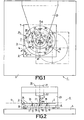
- Figs. 1 and 2 represent a device 1 for determining deviations of a nominally planar surface 2 of a thin and, in essence, circular disk-shaped object, that is a wafer 3, relative to a reference plane 4.
- the reference plane 4 is indicated by a dash-and-dot line in Fig. 2 .
- the wafer 3 is shown exaggeratedly large in its thickness. Furthermore, it should be observed that the wafer 3 in Fig. 2 is shown to be perfectly flat. In practice, however, the wafer may have deviations from a totally flat form, so that the nominally planar surface 2 of the wafer shows deviations from the reference plane 4.
- the device 1 has a stable base plate 5.
- the device 1 further has support means 6.
- the support means 6 have a carrier plate 7 which can be adjusted relative to the base plate 5 by bearing means 8 schematically shown as balls in the way that the carrier plate 7 can be adjusted relative to the base plate 5 both in the direction of a double arrow 9 and in the direction of a double arrow 10. In this way it is achieved that the carrier plate 7 can be taken to the desired position relative to the base plate 5.
- the support means 6 further include three support members 11, 12 and 13 which are formed by pins which are connected to the carrier plate 7 in a manner not shown.
- the free ends of the support members 11, 12 and 13 formed by pins are shown rounded off and lie in a plane that runs parallel with the reference plane 4.
- the three support members 11, 12 and 13 lie on a circle K that has a center M.
- the support members 11, 12 and 13 can be adjusted to each other in a way that each of the three support members 11, 12 and 13 can be adjusted exactly in a radial direction 14, 15 and 16 relative to the center M of the circle K, as is indicated by arrows in Fig. 1 .
- the wafer 3 can be supported in the area of three, in essence, point-shaped support positions 17, 18 and 19 and can be positioned with its surface 2 in a position that does not change relative to the reference plane 4.
- the device 1 further has detection means 20 by which deviations of the nominally planar surface 2 relative to the reference plane 4 can be detected.
- the detection means 20 include an optical microscope 21 which can be adjusted with adjusting means (not shown) of the detection means 20 in parallel with the direction of a double arrow 22.
- the direction of the double arrow 22 is exactly perpendicular to the reference plane 4.
- the detection means 20 are suspended from a carrier boom 23, which is connected to the base plate 5.
- a light beam LB schematically shown in Fig. 2 can be generated with the aid of the microscope, which light beam can be exactly focused on the surface 2 of the wafer 3, as is shown in Fig. 2 .
- the wafer 3 to be measured is either manually or automatically inserted into the device 1 and put on the three support members 11, 12 and 13, so that a positioning surface 24 on the wafer 3 lies exactly diagonally across from the second support member 18 relative to the center M.
- the carrier plate 7 together with the wafer 3 supported by the support members 17, 18 and 19 is brought to the position shown in Figs. 1 and 2 in which the center M of the circle K, which here exactly corresponds to the center of the wafer 3, which is ensured by separate positioning means not shown, however, in Figs. 1 and 2 , is exactly aligned with the light beam LB.
- the light beam LB in the surface center OM of the wafer 3 is exactly focused on the surface 2 of the wafer 3, which leads to the fact that the microscope 21 is adjusted in parallel with the direction of the double arrow 22.
- the microscope 21 takes up a certain relative position, in the present case a certain height position relative to the reference plane 4 through the surface center OM, thus the hit spot of the light beam LB on the surface. This lays down a start position of the microscope 21 relative to the height above the reference plane 4 and thus also the reference plane 4 itself.
- the carrier plate 7 together with the wafer 3 supported here by the support members 17, 18 and 19, is adjusted to the relative position indicated by dash-and-dot lines in Fig. 1 relative to the base plate 5 and thus also relative to the microscope 21.
- the result of this is that the light beam LB occurs from now on at the hit spot of the surface 2 of the wafer 3 indicated in Figs. 1 and 2 by the reference 25. It is assumed that within the area of the hit spot 25 of the surface 2 there is a deviation of the surface 2 relative to the reference plane 4, that is that the surface 2 in the area of the hit spot 25 lies above the reference plane 4. With these ratios the light beam LB is no longer exactly focused on the hit spot 25, which is determined with the aid of the microscope 21.
- the microscope 21 is from then on adjusted in parallel with the direction of the double arrow 22 until the light beam LB at the hit spot 25 is focused equally exactly on the surface 2.
- the microscope 21 is shifted relative to its start position found after the reference plane 4 was determined by a certain stroke parallel with the direction of the arrow 22.
- This stroke represents a measure for the deviation of the surface 2 at the hit spot 25 relative to the reference plane 4.
- the deviation of the nominally planar surface 2 relative to the reference plane 4 is determined in the hit spot 25.
- the operation described hereinbefore with respect to the hit spot 25 is repeated for a desired number of other hit spots of the surface 2 of the wafer 3, while a measuring result is obtained for each of these hit spots.
- the three support members 11, 12 and 13 on the carrier plate 7 are advantageously provided so that the three support members 11, 12 and 13 have such a relative position to each other that each support member 11, 12 and 13 is positioned, in essence, underneath the center of gravity 26, 27 and 28 respectively, of a circle sector 29, 30 and 31 that stretches out over an angular region of 120° of the in essence circular wafer 3, which wafer can be supported by the three support members 1 l, 12 and 13.
- This is achieved in that in the device 1 the radius r of the circle K at which the support members 11, 12 and 13 are positioned, has a value that results from the radius R of the wafer 3 via the equation r 0.55R.
- each support member 11, 12 and 13 lies underneath the point of gravity 26, 27 and 28 of a circle sector 29, 30 and 31 respectively, there is achieved in a very simple manner and without additional means that the influence of gravity on the measuring results, which can be determined when deviations of nominally planar surfaces 2 of the wafer 3 relative to the reference plane 4 can be detected, may practically be discarded, because based on the advantageous arrangement of the support members 11, 12 and 13 and as a result of the advantageous distribution of the support members 17, 18, 19 over the wafer 3, there is practically no parasitic warp of the wafer 3 caused by the influences of gravity.
- the support members 11, 12 and 13 can be radially adjusted, the support members 11, 12 and 13 can easily be adjusted to different radial positions and thus easily be adapted to wafers of different diameters.
- the invention is not restricted to the example of embodiment described above.
- a device according to the invention may also be included differently arranged support means which include three support members arranged according to the invention.
- detection means may be provided, for example, detection means which are suitable for performing an electrically capacitive measurement or detection means operating with laser beams as discussed, for example, in patent document DE 42 31 205 A1 also cited above.
- detection means which are suitable for performing an electrically capacitive measurement or detection means operating with laser beams as discussed, for example, in patent document DE 42 31 205 A1 also cited above.
- not only wafers, but also other disk-shaped objects can be measured exactly as regards the surface variation.
Landscapes
- Physics & Mathematics (AREA)
- General Physics & Mathematics (AREA)
- Testing Or Measuring Of Semiconductors Or The Like (AREA)
- Container, Conveyance, Adherence, Positioning, Of Wafer (AREA)
- Length Measuring Devices With Unspecified Measuring Means (AREA)
- Length Measuring Devices By Optical Means (AREA)
- Liquid Deposition Of Substances Of Which Semiconductor Devices Are Composed (AREA)
Abstract
Description
- The invention relates to a method as defined in the pre-characterizing part of
claim 1. - The invention further relates to a device as defined in the pre-characterizing part of
claim 3. - Such a method and such a device have for years been used by the applicants and are therefore known. The known solutions are provided and arranged for measuring wafers, so that an object to be measured is formed by a wafer. With the known solutions the support members and, consequently, the support positions are arranged in a more or less arbitrary position relative to each other. The main reason for this lies in the fact that the known solutions are provided for determining deviations of a nominally planar upper surface of a thin and, in essence, circular disk-shaped object, that is, a wafer, relative to a reference plane for which fact the wafer is thin and has a thickness, for example, in the region of 200 µm or more, but has nevertheless a thickness, that is the thickness of about 200 µm or more, with which practically no parasitic warpage occurs that can be attributed to the influences of gravity on the wafer. The known solutions are unsuitable for thinner wafers, because parasitic warpage occurs owing to gravity, which warpage leads to additional deviations of the nominally planar surfaces of such a wafer relative to a reference plane, which leads to erroneous measuring results with the known solutions. Since in practice, however, there is a tendency to come to ever thinner wafers, there is a problem that for such thinner wafers no satisfactory measuring results can be achieved with the known solutions with regard to finding deviations in a surface of a wafer relative to a reference plane.
- With regard to a known method and a known device, also the publication of patent document
DE 42 31 205 Al may be referred to in this respect. This document has also disclosed the use of three support members lying in the three corners of an equilateral triangle. However, no information is given about the positions of the three support members relative to the object to be measured, that is to a composite body. - It is an object of the invention to avoid the above-defined problems or at least reduce them to such an extent that in practice no detrimental problems occur and an improved method and an improved device are created.
- To achieve the above-defined object of the invention, for a method according to the pre-characterizing part of
claim 1, the characteristic features according to the characterizing part ofclaim 1 are provided. - To achieve the above-defined object of the invention for a device according to the pre-characterizing part of
claim 3, the characteristic features according to the characterizing part ofclaim 3 are provided. - Providing the characteristic features according to the invention achieves in an extremely simple manner and without additional means that the influence of gravity on the results of the measurement, which can be determined when deviations from a nominally planar surface of a thin and, in essence, circular disk-shaped object are measured relative to a reference plane, can be practically ignored because, based on the invented arrangement of the support members and as a result of the support positions of the object, practically no parasitic warp of the object owing to the influences of gravity occurs.
- With a device according to the invention it has proved to be highly advantageous when, additionally, the characteristic feature according to claim 4 is provided. In this manner the device can be adapted very simply to different sizes, thus to different diameters of circular disk-shaped objects.
- The above-defined aspects and further aspects of the invention will be evident from the example of embodiment to be described hereinafter and will be explained with reference to this example of embodiment.
- These and other aspects of the invention are apparent from and will be elucidated with reference to the embodiments described hereinafter.
-
-
Fig. 1 shows in a highly diagrammatic manner in plan view a device in accordance with an example of embodiment of the invention, and -
Fig. 2 shows the device shown inFig. 1 in side view. -
Figs. 1 and 2 represent adevice 1 for determining deviations of a nominallyplanar surface 2 of a thin and, in essence, circular disk-shaped object, that is awafer 3, relative to a reference plane 4. The reference plane 4 is indicated by a dash-and-dot line inFig. 2 . Thewafer 3 is shown exaggeratedly large in its thickness. Furthermore, it should be observed that thewafer 3 inFig. 2 is shown to be perfectly flat. In practice, however, the wafer may have deviations from a totally flat form, so that the nominallyplanar surface 2 of the wafer shows deviations from the reference plane 4. - The
device 1 has astable base plate 5. Thedevice 1 further has support means 6. The support means 6 have acarrier plate 7 which can be adjusted relative to thebase plate 5 by bearing means 8 schematically shown as balls in the way that thecarrier plate 7 can be adjusted relative to thebase plate 5 both in the direction of a double arrow 9 and in the direction of a double arrow 10. In this way it is achieved that thecarrier plate 7 can be taken to the desired position relative to thebase plate 5. - The support means 6 further include three
support members carrier plate 7 in a manner not shown. The free ends of thesupport members support members support members support members radial direction Fig. 1 . - With the aid of the three
support members wafer 3 can be supported in the area of three, in essence, point-shaped support positions surface 2 in a position that does not change relative to the reference plane 4. - The
device 1 further has detection means 20 by which deviations of the nominallyplanar surface 2 relative to the reference plane 4 can be detected. In the case at hand, the detection means 20 include anoptical microscope 21 which can be adjusted with adjusting means (not shown) of the detection means 20 in parallel with the direction of adouble arrow 22. The direction of thedouble arrow 22 is exactly perpendicular to the reference plane 4. The detection means 20 are suspended from acarrier boom 23, which is connected to thebase plate 5. - A light beam LB schematically shown in
Fig. 2 can be generated with the aid of the microscope, which light beam can be exactly focused on thesurface 2 of thewafer 3, as is shown inFig. 2 . - The following shows the way of operation of the
device 1 shown inFigs. 1 and 2 when a method of determining deviations of a nominallyplanar surface 2 of thewafer 3 from a reference plane 4 is described: - The
wafer 3 to be measured is either manually or automatically inserted into thedevice 1 and put on the threesupport members positioning surface 24 on thewafer 3 lies exactly diagonally across from thesecond support member 18 relative to the center M. - Furthermore, the
carrier plate 7 together with thewafer 3 supported by thesupport members Figs. 1 and 2 in which the center M of the circle K, which here exactly corresponds to the center of thewafer 3, which is ensured by separate positioning means not shown, however, inFigs. 1 and 2 , is exactly aligned with the light beam LB. - Furthermore, the light beam LB in the surface center OM of the
wafer 3 is exactly focused on thesurface 2 of thewafer 3, which leads to the fact that themicroscope 21 is adjusted in parallel with the direction of thedouble arrow 22. Once the light beam LB in the surface center OM is exactly focused on thesurface 2, themicroscope 21 takes up a certain relative position, in the present case a certain height position relative to the reference plane 4 through the surface center OM, thus the hit spot of the light beam LB on the surface. This lays down a start position of themicroscope 21 relative to the height above the reference plane 4 and thus also the reference plane 4 itself. - Furthermore, the
carrier plate 7 together with thewafer 3 supported here by thesupport members Fig. 1 relative to thebase plate 5 and thus also relative to themicroscope 21. The result of this is that the light beam LB occurs from now on at the hit spot of thesurface 2 of thewafer 3 indicated inFigs. 1 and 2 by the reference 25. It is assumed that within the area of the hit spot 25 of thesurface 2 there is a deviation of thesurface 2 relative to the reference plane 4, that is that thesurface 2 in the area of the hit spot 25 lies above the reference plane 4. With these ratios the light beam LB is no longer exactly focused on the hit spot 25, which is determined with the aid of themicroscope 21. Consequently, themicroscope 21 is from then on adjusted in parallel with the direction of thedouble arrow 22 until the light beam LB at the hit spot 25 is focused equally exactly on thesurface 2. Once the focused state is reached, themicroscope 21 is shifted relative to its start position found after the reference plane 4 was determined by a certain stroke parallel with the direction of thearrow 22. This stroke represents a measure for the deviation of thesurface 2 at the hit spot 25 relative to the reference plane 4. In this manner the deviation of the nominallyplanar surface 2 relative to the reference plane 4 is determined in the hit spot 25. The operation described hereinbefore with respect to the hit spot 25 is repeated for a desired number of other hit spots of thesurface 2 of thewafer 3, while a measuring result is obtained for each of these hit spots. - Based on all the measuring results, very accurate conclusions can be drawn from the surface ratios in the area of the
surface 2 of thewafer 3. - With the device as shown in
Figs. 1 and 2 , the threesupport members carrier plate 7 are advantageously provided so that the threesupport members support member gravity circle sector circular wafer 3, which wafer can be supported by the threesupport members device 1 the radius r of the circle K at which thesupport members wafer 3 via the equation r = 0.55R. - Based on the fact that each
support member gravity circle sector planar surfaces 2 of thewafer 3 relative to the reference plane 4 can be detected, may practically be discarded, because based on the advantageous arrangement of thesupport members support members wafer 3, there is practically no parasitic warp of thewafer 3 caused by the influences of gravity. - Since the
support members support members - The invention is not restricted to the example of embodiment described above. In a device according to the invention may also be included differently arranged support means which include three support members arranged according to the invention. Furthermore, also different detection means may be provided, for example, detection means which are suitable for performing an electrically capacitive measurement or detection means operating with laser beams as discussed, for example, in patent document
DE 42 31 205 A1 also cited above. Furthermore, not only wafers, but also other disk-shaped objects can be measured exactly as regards the surface variation.
Claims (5)
- A method of determining deviations of a nominally planar surface (2) of a thin and, in essence, circular disk-shaped object (3) relative to a reference plane (4)
in which the object (3) is supported by support means (6) in the area of three, in essence, point-shaped support positions (17, 18, 19) and is positioned with its surface (2) in a constant position relative to the reference plane (4) and
in which deviations of the nominally planar surface (2) relative to the reference plane (4) are detected by detection means (20),
characterized in that
the object (3) is supported in the area of such three support positions (17, 18, 19) of which each support position (17, 18, 19) is located, in essence, underneath the center of gravity (26, 27, 28) of a circle sector (29, 30, 31) that stretches out over an angular region of 120° of the, in essence, circular disk-shaped object (3). - A method as claimed in claim 1, characterized
in that as an object (3) a wafer (3) is supported in the area of such three support positions (17, 18, 19). - A device (1) for determining deviations of a nominally planar surface (2) of a thin and, in essence, circular disk-shaped object (3) relative to a reference plane (4),
which device (1) comprises support means (6) which have three support members (11, 12, 13) with the aid of which the object (3) can be supported by three, in essence, point-shaped support positions (17, 18, 19) and with its surface (2) can be positioned in a constant position relative to the reference plane (4), and
which device (1) comprises detection means (20) with the aid of which deviations of the nominally planar surface (2) relative to the reference plane (4) can be detected,
characterized in that
the three support members (11, 12, 13) have such a position relative to each other that each support member (11, 12, 13) is located, in essence, underneath the center of gravity (26, 27, 28) of a circle sector (29, 30, 31) extending over an angular range of 120° of the, in essence, circular disk-shaped object (3) which can be supported with the aid of the three support members (11, 12, 13). - A device (1) as claimed in claim 3, characterized
in that the three support members (11, 12, 13) can be adjusted relative to each other. - A device (1) as claimed in claim 3, characterized
in that the device (1) is arranged for determining deviations of a nominally planar surface (2) of a wafer (3) from a reference plane (4).
Priority Applications (1)
| Application Number | Priority Date | Filing Date | Title |
|---|---|---|---|
| EP00962314A EP1125096B1 (en) | 1999-08-31 | 2000-08-14 | Method of and device for determining the warpage of a wafer |
Applications Claiming Priority (4)
| Application Number | Priority Date | Filing Date | Title |
|---|---|---|---|
| EP99890278 | 1999-08-31 | ||
| EP99890278 | 1999-08-31 | ||
| PCT/EP2000/007920 WO2001016559A1 (en) | 1999-08-31 | 2000-08-14 | Method of and device for determining the warpage of a wafer |
| EP00962314A EP1125096B1 (en) | 1999-08-31 | 2000-08-14 | Method of and device for determining the warpage of a wafer |
Publications (2)
| Publication Number | Publication Date |
|---|---|
| EP1125096A1 EP1125096A1 (en) | 2001-08-22 |
| EP1125096B1 true EP1125096B1 (en) | 2008-07-16 |
Family
ID=8244006
Family Applications (1)
| Application Number | Title | Priority Date | Filing Date |
|---|---|---|---|
| EP00962314A Expired - Lifetime EP1125096B1 (en) | 1999-08-31 | 2000-08-14 | Method of and device for determining the warpage of a wafer |
Country Status (8)
| Country | Link |
|---|---|
| US (1) | US6567169B1 (en) |
| EP (1) | EP1125096B1 (en) |
| JP (1) | JP2003508736A (en) |
| KR (1) | KR100728402B1 (en) |
| AT (1) | ATE401550T1 (en) |
| DE (1) | DE60039491D1 (en) |
| TW (1) | TW544510B (en) |
| WO (1) | WO2001016559A1 (en) |
Families Citing this family (3)
| Publication number | Priority date | Publication date | Assignee | Title |
|---|---|---|---|---|
| JP4469462B2 (en) * | 2000-05-25 | 2010-05-26 | 株式会社ニコン | Carrier shape measuring machine |
| EP1907791A4 (en) * | 2005-07-27 | 2009-12-23 | Corning Inc | Apparatus and method for measuring a glass sheet |
| WO2021181906A1 (en) * | 2020-03-09 | 2021-09-16 | 村田機械株式会社 | Flatness measurement unit |
Family Cites Families (10)
| Publication number | Priority date | Publication date | Assignee | Title |
|---|---|---|---|---|
| US2641958A (en) * | 1951-01-09 | 1953-06-16 | Theodor W Zobel | Method and test equipment for measuring the quality of glass surfaces of unusually large dimensions under different supporting and loading conditions |
| JPS549903B2 (en) * | 1973-03-31 | 1979-04-28 | ||
| FR2494428A1 (en) * | 1980-11-18 | 1982-05-21 | Jacquot Jules | Measuring stage with high sensitivity for microscope - uses electromagnetic fields and laser optical system for position control of stage floating on mercury |
| JP2704734B2 (en) * | 1988-09-05 | 1998-01-26 | キヤノン株式会社 | Stage positioning correction method and apparatus |
| US5424552A (en) * | 1991-07-09 | 1995-06-13 | Nikon Corporation | Projection exposing apparatus |
| DE4231205A1 (en) | 1992-09-18 | 1994-03-24 | Siemens Ag | Bend-inducing internal stress determination in coated substrate - by surface curvature measurement using scanning probe of film thickness measuring device |
| US6122036A (en) * | 1993-10-21 | 2000-09-19 | Nikon Corporation | Projection exposure apparatus and method |
| JP3401769B2 (en) * | 1993-12-28 | 2003-04-28 | 株式会社ニコン | Exposure method, stage device, and exposure device |
| US5671054A (en) * | 1995-07-18 | 1997-09-23 | Nikon Corporation | Method and apparatus for measuring position of pattern formed on a substrate having a thickness |
| US5924058A (en) * | 1997-02-14 | 1999-07-13 | Applied Materials, Inc. | Permanently mounted reference sample for a substrate measurement tool |
-
2000
- 2000-08-14 EP EP00962314A patent/EP1125096B1/en not_active Expired - Lifetime
- 2000-08-14 WO PCT/EP2000/007920 patent/WO2001016559A1/en not_active Ceased
- 2000-08-14 KR KR1020017005288A patent/KR100728402B1/en not_active Expired - Fee Related
- 2000-08-14 DE DE60039491T patent/DE60039491D1/en not_active Expired - Lifetime
- 2000-08-14 AT AT00962314T patent/ATE401550T1/en not_active IP Right Cessation
- 2000-08-14 JP JP2001520066A patent/JP2003508736A/en not_active Withdrawn
- 2000-08-29 US US09/649,939 patent/US6567169B1/en not_active Expired - Lifetime
- 2000-09-21 TW TW089119471A patent/TW544510B/en not_active IP Right Cessation
Also Published As
| Publication number | Publication date |
|---|---|
| KR100728402B1 (en) | 2007-06-13 |
| ATE401550T1 (en) | 2008-08-15 |
| KR20010085968A (en) | 2001-09-07 |
| EP1125096A1 (en) | 2001-08-22 |
| DE60039491D1 (en) | 2008-08-28 |
| WO2001016559A1 (en) | 2001-03-08 |
| US6567169B1 (en) | 2003-05-20 |
| JP2003508736A (en) | 2003-03-04 |
| TW544510B (en) | 2003-08-01 |
Similar Documents
| Publication | Publication Date | Title |
|---|---|---|
| US4177568A (en) | Measurement head | |
| US4679937A (en) | Self leveling transmitter for laser alignment systems | |
| GB2035610A (en) | Wafer projection aligner | |
| US20130068034A1 (en) | Micromaterial strain measurement apparatus and method therefor techinical field | |
| US6342705B1 (en) | System for locating and measuring an index mark on an edge of a wafer | |
| US20020016650A1 (en) | Robot alignment system and method | |
| US20080208523A1 (en) | Method of determining geometric parameters of a wafer | |
| US20170160085A1 (en) | Levelness detecting device and method, levelness adjusting device and method | |
| US3999866A (en) | Wafer test system with integrated calibration | |
| US6567169B1 (en) | Method of and device for determining the warpage of a wafer | |
| JP5829211B2 (en) | Method and apparatus for measuring the deformation of a disk workpiece, in particular a molded wafer | |
| JP2968956B2 (en) | Thickness and / or warpage measuring device and method of using the same | |
| JP4663378B2 (en) | Shape measuring apparatus and method | |
| US7750295B2 (en) | Extractor for an microcolumn, an alignment method for an extractor aperture to an electron emitter, and a measuring method and an alignment method using thereof | |
| US5436721A (en) | Wafer tilt gauge | |
| US6255664B1 (en) | Sensor for measuring degree of flatness | |
| KR100344221B1 (en) | Apparatus for measuring tension of wafer clamp | |
| US7251988B2 (en) | Topography analyzing system | |
| JP2567951Y2 (en) | Hardness measuring device | |
| EP3911138A1 (en) | Back-up pin state confirmation system for component mounting apparatus | |
| RU1770730C (en) | Method and device for measuring geometrical parameters of plates | |
| CN115127457B (en) | Detection apparatus, system, method for focusing ring and plasma processing apparatus | |
| JPS61214518A (en) | Sample placing device for electron beam lithography equipment | |
| JP2644257B2 (en) | Beam detection target | |
| JP2005024405A (en) | Method for measuring film thickness of coated ceramic member, apparatus therefor, and manufacturing method for coated ceramic member |
Legal Events
| Date | Code | Title | Description |
|---|---|---|---|
| PUAI | Public reference made under article 153(3) epc to a published international application that has entered the european phase |
Free format text: ORIGINAL CODE: 0009012 |
|
| AK | Designated contracting states |
Kind code of ref document: A1 Designated state(s): AT BE CH CY DE DK ES FI FR GB GR IE IT LI LU MC NL PT SE |
|
| 17P | Request for examination filed |
Effective date: 20010910 |
|
| RBV | Designated contracting states (corrected) |
Designated state(s): AT DE FR GB IT |
|
| RAP1 | Party data changed (applicant data changed or rights of an application transferred) |
Owner name: NXP B.V. |
|
| GRAP | Despatch of communication of intention to grant a patent |
Free format text: ORIGINAL CODE: EPIDOSNIGR1 |
|
| GRAS | Grant fee paid |
Free format text: ORIGINAL CODE: EPIDOSNIGR3 |
|
| GRAA | (expected) grant |
Free format text: ORIGINAL CODE: 0009210 |
|
| AK | Designated contracting states |
Kind code of ref document: B1 Designated state(s): AT DE FR GB IT |
|
| REG | Reference to a national code |
Ref country code: GB Ref legal event code: FG4D |
|
| REF | Corresponds to: |
Ref document number: 60039491 Country of ref document: DE Date of ref document: 20080828 Kind code of ref document: P |
|
| PG25 | Lapsed in a contracting state [announced via postgrant information from national office to epo] |
Ref country code: AT Free format text: LAPSE BECAUSE OF FAILURE TO SUBMIT A TRANSLATION OF THE DESCRIPTION OR TO PAY THE FEE WITHIN THE PRESCRIBED TIME-LIMIT Effective date: 20080716 |
|
| PLBE | No opposition filed within time limit |
Free format text: ORIGINAL CODE: 0009261 |
|
| STAA | Information on the status of an ep patent application or granted ep patent |
Free format text: STATUS: NO OPPOSITION FILED WITHIN TIME LIMIT |
|
| 26N | No opposition filed |
Effective date: 20090417 |
|
| PG25 | Lapsed in a contracting state [announced via postgrant information from national office to epo] |
Ref country code: IT Free format text: LAPSE BECAUSE OF FAILURE TO SUBMIT A TRANSLATION OF THE DESCRIPTION OR TO PAY THE FEE WITHIN THE PRESCRIBED TIME-LIMIT Effective date: 20080716 |
|
| PGFP | Annual fee paid to national office [announced via postgrant information from national office to epo] |
Ref country code: GB Payment date: 20120726 Year of fee payment: 13 |
|
| REG | Reference to a national code |
Ref country code: GB Ref legal event code: 732E Free format text: REGISTERED BETWEEN 20121108 AND 20121114 |
|
| PGFP | Annual fee paid to national office [announced via postgrant information from national office to epo] |
Ref country code: DE Payment date: 20120831 Year of fee payment: 13 Ref country code: FR Payment date: 20120809 Year of fee payment: 13 |
|
| REG | Reference to a national code |
Ref country code: DE Ref legal event code: R082 Ref document number: 60039491 Country of ref document: DE Representative=s name: MUELLER-BORE & PARTNER PATENTANWAELTE, EUROPEA, DE |
|
| REG | Reference to a national code |
Ref country code: DE Ref legal event code: R081 Ref document number: 60039491 Country of ref document: DE Owner name: CALLAHAN CELLULAR L.L.C., US Free format text: FORMER OWNER: NXP B.V., EINDHOVEN, NL Effective date: 20130211 Ref country code: DE Ref legal event code: R082 Ref document number: 60039491 Country of ref document: DE Representative=s name: MUELLER-BORE & PARTNER PATENTANWAELTE, EUROPEA, DE Effective date: 20130211 Ref country code: DE Ref legal event code: R082 Ref document number: 60039491 Country of ref document: DE Representative=s name: MUELLER-BORE & PARTNER PATENTANWAELTE PARTG MB, DE Effective date: 20130211 |
|
| REG | Reference to a national code |
Ref country code: FR Ref legal event code: TP Owner name: CALLAHAN CELLULAR L.L.C., US Effective date: 20130724 |
|
| GBPC | Gb: european patent ceased through non-payment of renewal fee |
Effective date: 20130814 |
|
| PG25 | Lapsed in a contracting state [announced via postgrant information from national office to epo] |
Ref country code: DE Free format text: LAPSE BECAUSE OF NON-PAYMENT OF DUE FEES Effective date: 20140301 |
|
| REG | Reference to a national code |
Ref country code: DE Ref legal event code: R119 Ref document number: 60039491 Country of ref document: DE Effective date: 20140301 |
|
| REG | Reference to a national code |
Ref country code: FR Ref legal event code: ST Effective date: 20140430 |
|
| PG25 | Lapsed in a contracting state [announced via postgrant information from national office to epo] |
Ref country code: GB Free format text: LAPSE BECAUSE OF NON-PAYMENT OF DUE FEES Effective date: 20130814 |
|
| PG25 | Lapsed in a contracting state [announced via postgrant information from national office to epo] |
Ref country code: FR Free format text: LAPSE BECAUSE OF NON-PAYMENT OF DUE FEES Effective date: 20130902 |