TECHNICAL FIELD
-
The present invention relates to a magnetoresistive device and a
method for producing the same, and a magnetic component.
BACKGROUND ART
-
A TMR (tunnel magnetic resistance) device is a device in which a
very thin insulating layer is inserted between two ferromagnetic layers. A
TMR device uses the phenomenon that the tunneling current flowing
through the insulating layer is changed by the relative angle of
magnetization of each metal element M.
-
It has been expected in theory that when using a ferromagnetic
metal element M having a high spin polarizability such as Fe or FeCO for
the ferromagnetic layers, a high rate of change in magnetic resistance of at
least 35 % is obtained (M. Jullier, Phs. Lett. 54A (1975) 225). However, a
high MR (magneto resistance) has not been possible to realize.
-
Recently, Miyazaki et al. reported that they produced an insulating
layer of alumina by natural oxidation in the air, and obtained a high rate of
change in MR (T. Miyazaki and N. Tezuka, J. Magn. Magn. Mater. 139
(1995) L231). With this report, active development of TMR materials and
TMR devices has started.
-
The recently reported methods for producing insulating layers
showing a high MR are classified largely into two methods. One is a
natural oxidation method in which an aluminum film formed on a
ferromagnetic film is oxidized in the air or in pure oxygen (Tsuge et al.,
Document of the 103rd Workshop by the Society of Applied Magnetics of
Japan, p. 119, (1998)). The other is a plasma oxidation method in which an
aluminum film formed on a ferromagnetic film is oxidized in an oxygen
plasma (J. S. Moodera et al. Phy. Rev. Lett., 74, 3273 (1995)).
-
To obtain a high MR, these TMR devices use a transition metal
showing a high spin polarizability such as Fe or CoFe for the lower
ferromagnetic layer on which the aluminum film is formed.
-
Because the current flowing in a TMR device is mainly a tunneling
current through an insulating layer, the resistance of the device is
substantially high. Thus, when a TMR device is used as a reproducing
head or MRAM, S/N ratio decreases due to thermal noise, and threshold
frequency of a readout circuit decreases during a fast response.
-
To lower the resistance of the device, reducing the film thickness of
the alumina insulating layer could be considered. However, with a
conventional process for oxidizing an aluminum film, the lower
ferromagnetic film is likely to be oxidized beyond the aluminum film when
the aluminum film is thin. As a result, when antiferromagnetic materials
such as Fe2O3 and CoO are formed at the interface with the aluminum oxide
film by an excess oxidation reaction, for example, due to the interaction
with these antiferromagnetic oxides, tunneling electrons lose information of
magnetization direction with an external magnetic field.
-
On the other hand, when the aluminum film is not oxidized
completely and a portion of the aluminum film remains, the spin memory of
the tunneling electrons passing through the remaining aluminum film is
lost, and MR is reduced.
-
Furthermore, in conventional TMR devices, when a large bias is
applied, the rate of change in MR is decreased greatly due to generation of
magnon, etc.
-
Furthermore, conventional MR devices do not have a sufficient
thermal stability, and for example, when using them as MRAM, heat
deterioration such as decreased MR property is caused during post-annealing
of CMOS (at about 250 to 400 °C) or heating in the production of
MR heads (at about 250 °C), or during its use.
DISCLOSURE OF THE INVENTION
-
In view of the above-mentioned problems, it is an object of the
present invention to provide a new magnetoresistive device having a low
junction resistance and a high MR and a method for producing the same,
and a magnetic component.
-
To achieve the above object, the present invention provides a
magnetoresistive device including a high-resistivity layer, a first magnetic
layer and a second magnetic layer, the first magnetic layer and the second
magnetic layer being arranged so as to sandwich the high-resistivity layer,
wherein the high-resistivity layer is a barrier for passing tunneling
electrons between the first magnetic layer and the second magnetic layer,
and contains at least one element LONC selected from oxygen, nitrogen and
carbon; at least one layer A selected from the first magnetic layer and the
second magnetic layer contains at least one metal element M selected from
Fe, Ni and Co, and an element RCP different from the metal element M; and
the element RCP combines with the element LONC more easily in terms of
energy than the metal element M. In the magnetoresistive device of the
present invention, the element RCP contained in the layer A combines
selectively with the element LONC diffusing from the high-resistivity layer to
form a compound. Thus, in the magnetoresistive device of the present
invention, oxidation, nitriding or carbonization of the metal element M can
be inhibited, thereby preventing generation of a localized spin resulting in
spin inversion. Furthermore, when the element RCP in the layer A
combines with the element LONC to form a compound, the compound itself
functions as a part of the high-resistivity layer. In addition, because the
diffusion velocity of oxygen ions or nitrogen ions in the compound of the
element RCP and the element LONC is substantially lower than in the
magnetic films, the compound of the element RCP and the element LONC acts
as a layer to inhibit diffusion of excess oxygen or nitrogen. Therefore, in
the magnetoresistive device of the present invention, formation of a high-resistivity
layer having a larger thickness than necessary, resulting in an
increase in the resistance of the device, is inhibited. Thus, according to the
magnetoresistive device of the present invention, a device having a low
junction resistance and a high MR is obtained.
-
In the magnetoresistive device of the present invention, it is
preferable that the layer A contains the element RCP so that a concentration
of the element RCP is high on the side of the high-resistivity layer. When
the element RCP is in a solid solution state with a metal composed of the
metal element M, its spin polarizability is generally lower than that of the
single metal composed of the metal element M. However, by making the
concentration of the element RCP high on the side of the high-resistivity
layer in the layer A, the element RCP forms a compound, and the element RCP
and the metal element M are separated in phase. As a result, high spin
polarizability is obtained in the vicinity of the high-resistivity layer, which
has the greatest influence on the rate of change in magnetoresistance. The
spin polarizability can be increased by decreasing the concentration of the
element RCP as it is farther from the high-resistivity layer. The layer A
may have a two-layered structure such as an element RCP-containing Fe
layer/Fe layer from the side of the high-resistivity layer. The layer A also
may have a structure such as an element RCP-containing FeCo layer/FeCo
layer from the side of the high-resistivity layer.
-
In the magnetoresistive device of the present invention, it is
preferable that the element RCP is at least one element selected from Si, Ge,
Al, Ga, Cr, V, Nb, Ta, Ti, Zr, Hf, Mg and Ca. These elements have a larger
free energy in negative for forming oxides than the metal element M, and
selectively capture oxygen ions or nitrogen ions diffusing from the high-resistivity
layer. Among these elements, Si, Al, Cr and Ti have particularly
large diffusion constants in metal elements. Thus, these four elements
diffuse toward the side of the high-resistivity layer so that their
concentrations are high on the side of the high-resistivity layer, using as a
driving force the chemical potential gradient of the oxygen or nitrogen ions
generated when forming the high-resistivity layer. Therefore, a desirable
concentration gradient of the element RCP can be formed easily by using
these four elements. This self-diffusion of elements tends to appear more
remarkably when the high-resistivity layer is formed at a higher reaction
temperature.
-
In the magnetoresistive device of the present invention, it is
preferable that the layer A consists of Fe, Si and Al. Accordingly, a lower
resistance of the device can be obtained. Furthermore, the rate of change
in the magnetoresistance is increased, and the soft magnetic property of the
layer A is enhanced. Thus, a high MR is obtained at a low magnetic field.
-
In the magnetoresistive device of the present invention, it is
preferable that the element RCP forms a compound with the element LONC in
the vicinity of the high-resistivity layer in the layer A. Accordingly, the
spin polarizability in the vicinity of the high-resistivity layer is increased
due to phase separation with the metal element M, so that a
magnetoresistive device having a particularly high rate of change in
magnetoresistance is obtained.
-
In the magnetoresistive device of the present invention, it is
preferable that the second magnetic layer is formed after forming the high-resistivity
layer, and a portion of the high-resistivity layer contacting the
second magnetic layer contains an aluminum oxide as a main component.
Oxygen and nitrogen ions have a lower diffusion constant in an aluminum
oxide than in other oxides. Thus, according to the above structure,
diffusion of these ions through the high-resistivity layer can be inhibited
effectively when forming the high-resistivity layer. As a result, the
probability that the element RCP captures oxygen and nitrogen ions
diffusing through the high-resistivity layer increases, so that oxidation and
nitriding of the metal element M resulting in spin inversion can be inhibited.
Furthermore, according to the above structure, the thickness of the high-resistivity
layer is controlled easily. Furthermore, in the above structure,
it is preferable that a current is passed so that the first magnetic layer is
positive and the second magnetic layer is negative. Accordingly, diffusion
of oxygen ions is inhibited when a current is applied, so that the life of the
device can be extended.
-
In the magnetoresistive device of the present invention, it is
preferable that at least a portion of the high-resistivity layer is formed by
forming a film containing the metal element M and the element RCP, and
then reacting the surface of the film with the element LONC. Accordingly,
the element RCP in the first magnetic layer and the high-resistivity layer
form a thermally stable relationship, so that the reliability of the device at a
high temperature is increased. Furthermore, in this case, it is preferable
that a current is passed so that the first magnetic layer is negative and the
second magnetic layer is positive. Accordingly, diffusion of oxygen ions is
inhibited when a current is applied, so that the life of the device can be
extended.
-
Furthermore, the present invention provides a method for producing
a magnetoresistive device, including:
- (a) forming a first magnetic layer located on a substrate, and a
high-resistivity layer located on the first magnetic layer and containing at
least one element LONC selected from oxygen, nitrogen and carbon; and
- (b) forming a second magnetic layer on the high-resistivity layer;
wherein the first magnetic layer contains at least one metal element M
selected from Fe, Ni and Co, and an element RCP different from the metal
element M; and the element RCP combines with the element LONC more easily
in terms of energy than the metal element M. According to the method of
the present invention, a magnetoresistive device of the present invention
can be produced.
-
-
In the method of the present invention, it is preferable that the step
(a) includes:
- (a-1) forming a magnetic layer containing the metal element M on
the substrate, and
- (a-2) forming a layer B containing the element RCP on the magnetic
layer, and then reacting a portion of the layer B on the side of its surface
with the element LONC thereby to form the high-resistivity layer, and further
includes:
after the step (a-2) and before or after the step (b), allowing
unreacted parts of the element RCP in the layer B and the metal element M
in the magnetic layer to diffuse mutually by heating the substrate at a
temperature of at least 50 °C but not higher than 350 °C, thereby to form
the first magnetic layer in which the concentration of the element RCP
gradually increases to the side of the high-resistivity layer. Accordingly,
unreacted parts of the element RCP are allowed to diffuse into the first
magnetic layer, so that deletion of spin memory due to unreacted parts of
the element RCP can be prevented. -
-
In the method of the present invention, it is preferable that the step
(a) includes:
- (a-1) forming the first magnetic layer on the substrate; and
- (a-2) forming a layer C having a thickness of 0.1 nm to 2 nm and
containing the element RCP on the first magnetic layer, and then reacting
the layer C with the element LONC thereby to form the high-resistivity layer.
Accordingly, when forming the high-resistivity layer, the element RCP in the
first magnetic layer captures the element LONC diffusing from the high-resistivity
layer to form a compound. Thus, a magnetoresistive device
having a low junction resistance and a high MR is obtained.
-
-
In the method of the present invention, it is preferable that in the
step (a-2), the element RCP in the layer C is allowed to diffuse into the first
magnetic layer so that the concentration of the element RCP gradually
increases to the side of the high-resistivity layer in the first magnetic layer.
-
In the method of the present invention, it is preferable that the step
(a) includes:
- (a-1) forming the first magnetic layer on the substrate;
- (a-2) depositing the element RCP on the first magnetic layer in a gas
atmosphere containing the element LONC thereby to form the high-resistivity
layer. Accordingly, the magnetoresistive device of the present invention
can be produced easily.
-
-
In the method of the present invention, it is preferable that in the
step (a-2), the element RCP is allowed to diffuse into the first magnetic layer
so that the concentration of the element RCP gradually increases to the side
of the high-resistivity layer in the first magnetic layer.
-
In the method of the present invention, it is preferable that the step
(a) includes:
- (a-1) forming a magnetic layer containing the metal element M and
the element RCP on the substrate; and
- (a-2) reacting the surface of the magnetic layer with the element
LONC thereby to form the first magnetic layer and the high-resistivity layer.
According to this method, even when the surface of the magnetic layer is not
flat, a high-resistivity layer having an approximately uniform thickness can
be formed easily. Furthermore, in this method, it is preferable that in the
step (a-2), the element RCP is allowed to diffuse into the first magnetic layer
so that the concentration of the element RCP gradually increases to the side
of the high-resistivity layer in the first magnetic layer. Furthermore, in
this case, it is preferable that in the step (a-2), when reacting the surface of
the magnetic layer with the element LONC, the surface of the magnetic layer
is heated at a temperature of at least 50 °C but not higher than 800 °C. By
carrying out such a heating, the diffusion velocity of the element RCP can be
increased, and the time for forming the high-resistivity layer can be
shortened.
-
-
In the method of the present invention, it is preferable that in the
step (a), the first magnetic layer is formed by evaporation or sputtering so
that the concentration of the element RCP is high on the side of the high-resistivity
layer in the first magnetic layer. Accordingly, the concentration
distribution of the element RCP in the first magnetic layer can be controlled
easily by controlling the deposition rate of the element RCP.
-
Furthermore, the present invention provides a magnetic component
including a magnetoresistive device, wherein the magnetoresistive device is
obtained by heating the magnetoresistive device of the present invention at
a temperature of at least 200 °C. According to the magnetic component of
the present invention, each magnetic component easily can obtain an
arbitrary resistance meeting its use as well as a high MR. For example, a
resistance of several ten-ohms to several mega-ohms times square micron
for RA (resistance area) is required in MRAM. Also, a resistance of several
tens of milli-ohm to several ohms times square micron is required in a
magnetic head. Moreover, a high MR can be obtained even when its
surface is relatively rough.
BRIEF DESCRIPTION OF THE DRAWINGS
-
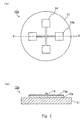
Fig. 1(a) is a plan view showing an example of a magnetoresistive
device of the present invention. Fig. 1(b) is a sectional view of the
magnetoresistive device of Fig. 1(a).
-
Fig. 2(a) is a plan view showing another example of a
magnetoresistive device of the present invention. Fig. 2(b) is a sectional
view of the magnetoresistive device of Fig. 2(a).
-
Fig. 3 is a process drawing showing an example of a method for
producing a magnetoresistive device of the present invention.
-
Fig. 4 is a process drawing showing another example of a method for
producing a magnetoresistive device of the present invention.
-
Fig. 5 is a process drawing showing still another example of a
method for producing a magnetoresistive device of the present invention.
-
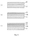
Fig. 6 is a process drawing showing still another example of a
method for producing a magnetoresistive device of the present invention.
-
Fig. 7(a) is a partially sectional view showing still another example
of a magnetoresistive device of the present invention. Fig. 7(b) is a
schematic illustration showing an arrangement of magnetic layers in the
magnetoresistive device of Fig. 7(a).
-
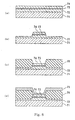
Fig. 8 is a process drawing showing a method for producing the
magnetoresistive device of Fig. 7.
-
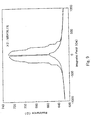
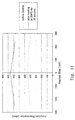
Fig. 9 is a graph showing a MR curve for a magnetoresistive device
of the present invention.
-
Fig. 10 is a graph showing an example of the applied bias
dependency of normalized MR for a magnetoresistive device of the present
invention.
-
Fig. 11 is a graph showing an example of the applied bias
dependency of the junction resistance for a magnetoresistive device of the
present invention.
-
Fig. 12 is a graph showing another example of the applied bias
dependency of normalized MR for a magnetoresistive device of the present
invention.
-
Fig. 13 is a graph showing another example of the applied bias
dependency of junction resistance for a magnetoresistive device of the
present invention.
-
Fig. 14 is a graph showing another example of a MR curve for a
magnetoresistive device of the present invention.
-
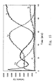
Fig. 15 is a graph showing an Auger depth profile of a junction for a
magnetoresistive device of the present invention.
-
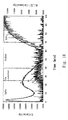
Fig. 16 is a magnification of the graph shown in Fig. 15.
-
Fig. 17 is a graph showing still another example of the applied bias
dependency of normalized MR for a magnetoresistive device of the present
invention.
-
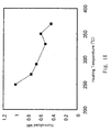
Fig. 18 is a graph showing a relation between the heating
temperature and normalized MR for a method for producing a
magnetoresistive device of the present invention.
BEST MODE FOR CARRYING OUT THE INVENTION
-
In the following, embodiments of the present invention are
described with reference to the drawings.
First Embodiment
-
In the first embodiment, an example of a magnetoresistive device of
the present invention is described.
-
Fig. 1(a) shows a plan view of a magnetoresistive device 10 of a first
embodiment. Fig. 1(b) shows a sectional view taken along the line X-X of
Fig. 1(a).
-
Referring to Fig. 1, a magnetoresistive device 10 includes a
substrate 11, and a first magnetic layer 12, a high-resistivity layer 13 and a
second magnetic layer 14 laminated one by one on the substrate 11. In
other words, the magnetoresistive device 10 includes the high-resistivity
layer 13, and the first magnetic layer 12 and the second magnetic layer 14
arranged so as to sandwich the high-resistivity layer 13.
-
Various substrates may be used for the substrate 11. Specifically,
for example, a single crystal (magnesia, sapphire, STO, etc.), polycrystal
(e.g. ATTIC substrate), amorphous (thermal oxide film of silicon), or
conductive substrate (or an oxide of alumina or silicon formed on a base)
may be employed. The substrate 11 is not limited to these examples, and
other substrates also may be used as long as the first magnetic layer 12 and
the second magnetic layer 14 are insulated. For example, when the
substrate 11 is a conductor, an additional insulator may be formed between
the first magnetic layer 12 and the second magnetic layer 14 in a place
other than the tunnel junction.
-
It is preferable that the surface roughness of the substrate 11 is not
more than 1 nm, particularly preferably not more than 0.5 nm. The
substrate 11 may have a lower electrode layer or a lower magnetic layer on
its surface as needed. The lower electrode layer herein referred to is an
electrode for current and voltage to measure the magnetic resistance of the
device, and a low-resistivity metal such as Pt, Au, Cu, Ru or Al may be used.
In this case, it is particularly preferable that the lower electrode layer
consists of a material containing at least 90 atomic % of Cu. Furthermore,
before forming the high-resistivity layer (non-magnetic layer), to smooth the
surface of the lower electrode layer, ions in a cluster form (e.g. cluster of an
inert gas such as Ar) may be irradiated at a low angle with respect to the
surface of the lower electrode layer. Furthermore, the first magnetic layer
12 may serve as the lower electrode layer.
-
Furthermore, a magnetic perovskite oxide, FeCo, Fe or the like
having high spin polarizability may be used for the lower magnetic layer.
Furthermore, when forming a spin valve magnetoresistive device, to make
the first magnetic layer 12 or the second magnetic layer 14 to be a pinned
layer, a conductive antiferromagnetic material consisting of a compound of
at least one element selected from Pt, Ir, Cr, Pd, Ru and Re; and Mn (e.g.
PtMn or IrMn) may be used. Also, Co-based alloy/Ru/Co-based alloy
known as a synthetic structure may be used. In this case, the Ru layer has
a thickness of 0.6 to 0.8 nm. The Co-based alloy contains at least 50 % Co,
and for example, Co, CoPt or CoPtCr may be used.
-
The first magnetic layer 12 and the second magnetic layer 14
essentially consist of magnetic metals and contain, for example, at least one
metal element M selected from Fe, Ni and Co. Specifically, these layers
contain, for example, Fe, Co, Ni, a FeCo alloy, a FeNi alloy or a CoFeNi alloy.
Particularly, it is preferable that the amount of nickel in the FeNi alloy is
from 30 to 80 %, and the amount of Co in the FeCo alloy is at least 10 %.
Furthermore, in the first magnetic layer 12, it is preferable that the element
RCP is included in these materials. Other than these materials, AMnSb (A
is at least one selected from Ni, Cu and Pt) also may be used. Furthermore,
materials such as LaSrMnO, CrO2 and Fe3O4 that are oxides but exhibit
high spin polarizability also may be used.
-
The high-resistivity layer (non-magnetic layer) 13 is a barrier for
passing tunneling electrons between the first magnetic layer 12 and the
second magnetic layer 14. The high-resistivity layer 13 may pass
thermoelectrons in addition to tunneling electrons. In the
magnetoresistive device 10, a current electrode and a voltage electrode are
connected to each of the first magnetic layer 12 and the second magnetic
layer 14, and a magnetic resistance is measured by a four-probe method.
In the magnetoresistive device 10, a tunneling current flows through a
portion where the first magnetic layer 12 and the second magnetic layer 14
cross each other. Hereinafter, the area of this crossing portion may be
referred to as a cross-sectional area of the device.
-
The high-resistivity layer 13 contains an element LONC that is at
least one selected from oxygen, nitrogen and carbon as a constituent
element. Specifically, a high-resistivity layer containing at least one
selected from an oxide, a nitride and a carbide may be used as the high-resistivity
layer 13. More specifically, for example, a layer consisting of a
high-resistivity material having a high bandgap of at least 1 eV such as
Al2O3, AlN, BN, SiO2, Si3N4, SiC, (AlGa)N or (AlB)N may be used.
Moreover, a layer consisting of a composite of these materials, or multiple
layers of these materials may be used. The amounts of oxygen, nitrogen
and carbon in these materials may deviate from their stoichiometric ratios
by about 5 %. Furthermore, the non-magnetic layer 13 may have a multi-layered
structure in which a layer (not more than 1 nm in thickness)
consisting of a non-magnetic metal material or a magnetic metal material is
sandwiched between high-resistivity materials. Furthermore, a layer (not
more than 0.5 nm in thickness) consisting of a non-magnetic metal may be
inserted in the high-resistivity layer 13. The thickness of the high-resistivity
layer 13 is, for example, from 0.2 nm to 5 nm, and particularly
preferably from 0.5 nm to 2.5 nm.
-
In the magnetoresistive device 10, at least one layer A (preferably
both layers) selected from the first magnetic layer 12 and the second
magnetic layer 14 contains at least one metal element M selected from Fe,
Ni and Co, and an element RCP different from the metal element M.
Specifically, for example, a magnetic layer consisting of Fe, Si and Al or a
layer containing the above-described magnetic materials and an element
RCP may be used as the layer A. It is preferable that the layer A contains at
least 0.1 atomic % of the element RCP, particularly preferably at least 10
atomic % of the element RCP. The element RCP in the layer A may be or may
not be in a solid solution state with the metal element M. The element RCP
in the layer A may form a compound by combining with the element LONC.
-
It is preferable that the layer A contains the element RCP so that the
concentration of the element RCP is high on the side of the high-resistivity
layer 13. In this case, the concentration of the element RCP may increase
gradually to the side of the high-resistivity layer 13. Also, the layer A may
have a two-layered structure consisting of a layer containing the element
RCP and a layer not containing the element RCP.
-
Furthermore, the second magnetic layer 14 may be formed after
forming the high-resistivity layer 13, and at least a portion of the high-resistivity
layer 13 contacting the second magnetic layer 14 may contain an
aluminum oxide as a main component. In this case, it is preferable that a
current is passed so that the first magnetic layer 12 is positive and the
second magnetic layer 14 is negative. For example, the aluminum oxide
may be Al2O3.
-
Furthermore, at least a portion of the high-resistivity layer 13 may
be formed by forming a film containing the metal element M and the
element RCP, and then reacting the surface of the film with the element LONC.
In this case, it is preferable that a current is passed so that the first
magnetic layer 12 is negative and the second magnetic layer 14 is positive.
-
The element RCP is characterized by that it combines with the
element LONC more easily in terms of energy than the metal element M.
For example, (1) an element having a larger free energy in negative for
forming an oxide by combining with one molecule of oxygen than the metal
element M, (2) an element having a larger free energy in negative for
forming a nitride by combining with one molecule of nitrogen than the
metal element M, or (3) an element having a larger free energy in negative
for forming a carbide by combining with one molecule of carbon than the
metal element M may be used as the element RCP. Specifically, at least one
element selected from Si, Ge, Al, Ga, Cr, V, Nb, Ta, Ti, Zr, Hf, Mg and Ca
may be used as the element RCP.
-
In the magnetoresistive device 10, when forming the high-resistivity
layer 13 or using the device, the element RCP in the layer A captures the
element LONC diffusing from the high-resistivity layer 13 to form a
compound. As a result, in the magnetoresistive device 10, formation of an
antiferromagnetic material such as Fe2O3 or CoO or a magnetic material
having low spin polarizability such as Fe4N or FeC in the layer A can be
prevented. Thus, according to the magnetoresistive device 10, the
thickness of the high-resistivity layer can be made sufficiently small, so that
a device having a low junction resistance and a high magnetic resistance
can be obtained.
-
The magnetoresistive device shown in Fig. 1 is only one example,
and the magnetoresistive device of the present invention may have other
structures. As an example of a structure different from the
magnetoresistive device 10, a plan view of the magnetoresistive device 10a
is shown in Fig. 2(a). Furthermore, a sectional view taken along the line
Y-Y of Fig. 2(a) is shown in Fig. 2(b).
-
Referring to Fig. 2, the magnetoresistive device 10a includes a
substrate 11, and a first magnetic layer 12a, a high-resistivity layer 13a and
a second magnetic layer 14 laminated one by one on the substrate 11. The
first magnetic layer 12a and the second magnetic layer 14 are arranged so
as to sandwich the high-resistivity layer 13a.
-
Because the substrate 11 and the second magnetic layer 14 are the
same as those in the magnetoresistive device 10, overlapped explanations
thereof are omitted. The high-resistivity layer 13a is formed by reacting a
portion of the first magnetic layer 12a with the element LONC, and has the
same function as the high-resistivity layer 13. That is, in the
magnetoresistive device 10a, at least a portion of the high-resistivity layer
13 is formed by forming a film containing the metal element M and the
element RCP, and then reacting the surface of the film with the element
LONC.
-
In the magnetoresistive device 10a, it is preferable that a current is
passed so that the first magnetic layer 12a is negative and the second
magnetic layer 14 is positive.
-
According to the magnetoresistive device 10a, the same effect as
that of the magnetoresistive device 10 is obtained.
Second Embodiment
-
In the second embodiment, an example of the method for producing
a magnetoresistive device according to the present invention is described.
With respect to the same parts and elements as those described in the first
embodiment, the same numerals are applied, and overlapped explanations
thereof are omitted.
-
The method of the second embodiment includes:
- (a) forming a first magnetic layer 12a located on a substrate 11, and
a high-resistivity layer 13 located on the first magnetic layer 12a and
containing at least one element LONC selected from oxygen, nitrogen and
carbon; and
- (b) forming a second magnetic layer 14 on the high-resistivity layer
13. The first magnetic layer 12a contains at least one metal element M
selected from Fe, Ni and Co, and contains an element RCP different from the
metal element M. As described in the first embodiment, the element RCP
combines with the element LONC more easily in terms of energy than the
metal element M. It is preferable that the second magnetic layer 14 also
contains the element RCP.
-
-
In the following, the above-mentioned method is described further
with more specific four methods. In Figs. 3 to 6, only the portion where the
first magnetic layer and the second magnetic layer cross each other is
illustrated.
[First Method]
-
Fig. 3 shows an example of the production process of the first
method. In the first method, first, as illustrated in Fig. 3(a), a magnetic
layer 32 containing a metal element M is formed on a substrate 11.
Specifically, a layer consisting of at least one selected from Fe, Ni and Co
may be used as the magnetic layer 32. The magnetic layer 32 may be
formed, for example, by a film-forming method such as evaporation using a
metal mask, sputtering, MBE, laser ablation, high-frequency magnetron
sputtering, direct current sputtering, facing target sputtering, or ion beam
sputtering. Any of the following layers such as a magnetic layer or a high-resistivity
layer also may be formed by the same film-forming method.
-
Then, as illustrated in Fig. 3(b), a layer B containing an element RCP
is formed on the magnetic layer 32. The layer B can be formed, for
example, using a metal mask having a square open hole.
-
Then, as illustrated in Fig. 3(c), a portion of the surface of the layer
B is allowed to react with an element LONC to form a high-resistivity layer 13.
That is, the high-resistivity layer 13 is formed by oxidizing, nitriding, or
carbonizing the element in the surface of the layer B. To react the surface
of the layer B with the element LONC, for example, the layer B may be
treated in a gas atmosphere containing the element LONC. Examples of the
gas atmosphere containing the element LONC include oxygen gas atmosphere,
oxygen plasma atmosphere, nitrogen gas atmosphere, nitrogen plasma
atmosphere, oxygen radical atmosphere, nitrogen radical atmosphere, ozone
atmosphere, and the like. In the step of Fig. 3(c), the kind of a gas, partial
pressure of a gas, plasma density, substrate temperature, and the like are
controlled to carry out the treatment.
-
Then, as illustrated in Fig. 3(d), by heating the substrate on which
the high-resistivity layer 13 is formed at a temperature of at least 50 °C but
not higher than 350 °C, unreacted parts of the element RCP not included in
the high-resistivity layer 13 are allowed to diffuse mutually with the metal
element M in the magnetic layer 32, thereby forming a first magnetic layer
32a containing the element RCP in which the concentration of the element
RCP gradually increases to the side of the high-resistivity layer 13.
-
Then, as illustrated in Fig. 3(e), a second magnetic layer 14 is
formed on the high-resistivity layer 13. The second magnetic layer 14 can
be formed by the same method as the magnetic layer 32. Thus, the
magnetoresistive device 10 described in the first embodiment can be
produced.
-
In the first method, heating of the substrate (diffusion of the
element RCP) may be carried out after forming the second magnetic layer 14.
The substrate also may be heated simultaneously with the step of forming
the magnetic layer 32, so that the element RCP is allowed to diffuse into the
magnetic layer 32 when forming the layer B. In this case, the outermost
surface of the layer B is oxidized with residual oxygen or water in the
vacuum device, etc. to form a high-resistivity layer. Thus, essentially, the
step of forming a high-resistivity layer, the step of forming a layer
consisting of unreacted RCP, and the step of diffusing unreacted RCP proceed
simultaneously. These steps are all included in the first method.
Furthermore, fine processing for forming the device also may be carried out
between these steps.
[Second Method]
-
In the second method, first, as illustrated in Fig. 4(a), a first
magnetic layer 12a is formed on a substrate 11.
-
Then, as illustrated in Fig. 4(b), a layer C having a thickness of 0.1
nm to 2 nm and containing an element RCP is formed on the first magnetic
layer 12a.
-
Then, as illustrated in Fig. 4(c), a high-resistivity layer 13 is formed
by reacting the layer C with an element LONC. That is, the high-resistivity
layer 13 is formed by oxidizing, nitriding, or carbonizing an element in the
layer C. This is the same as the step of Fig. 3(c). However, the entire
layer C is allowed to react with the element LONC in the second method.
-
Then, as illustrated in Fig. 4(d), a second magnetic layer 14 is
formed on the high-resistivity layer 13. Thus, the magnetoresistive device
10 described in the first embodiment can be produced.
-
It is preferable that the first magnetic layer 12a contains the
element RCP so that the concentration of the element RCP gradually
increases to the side of the high-resistivity layer 13. To form such a first
magnetic layer 12a, the element RCP may be allowed to diffuse into the first
magnetic layer 12a in the step of Fig. 4(b) or Fig. 4(c).
-
The first magnetic layer 12a also may be formed by evaporation or
sputtering in which the deposition rates of respective elements are changed
so that the concentration of the element RCP is high on the side of the high-resistivity
layer 13 (this also applies to the following methods).
[Third Method]
-
In the third method, first, as illustrated in Fig. 5(a), a first magnetic
layer 12a is formed on a substrate 11. This is the same as the step of Fig.
4(a).
-
Then, as illustrated in Fig. 5(b), a high-resistivity layer 13 is formed
by depositing an element RCP on the first magnetic layer 12a in a gas
atmosphere containing an element LONC. Examples of the gas atmosphere
containing an element LONC include oxygen gas atmosphere, oxygen plasma
atmosphere, nitrogen gas atmosphere, nitrogen plasma atmosphere, oxygen
radical atmosphere, nitrogen radical atmosphere, ozone atmosphere, and
the like.
-
In the step of Fig. 5(b), the element RCP may be allowed to diffuse
into the first magnetic layer 12a so that the concentration of the element
RCP in the first magnetic layer 12a gradually increases to the side of the
high-resistivity layer 13.
-
Then, as illustrated in Fig. 5(c), a second magnetic layer 14 is
formed. This is the same as the step of Fig. 4(d). Thus, the
magnetoresistive device 10 described in the first embodiment can be
produced.
[Fourth Method]
-
In the fourth method, as illustrated in Fig. 6(a), a magnetic layer 62
containing a metal element M and an element RCP is formed on a substrate
11. The magnetic layer 62 can be formed by the same method as the first
magnetic layer 12a.
-
Then, as illustrated in Fig. 6(b), by reacting the surface of the
magnetic layer 62 with an element LONC, a first magnetic layer 12a and a
high-resistivity layer 13 are formed. That is, in the step of Fig. 6(b), the
high-resistivity layer 13 is formed by oxidizing, nitriding, or carbonizing the
surface of the magnetic layer 62. To react the surface of the magnetic layer
62 with the element LONC, the magnetic layer 62 may be treated in a gas
atmosphere containing the element LONC in the same way as the step 4(c).
-
In the step of Fig. 6(b), it is preferable that the element RCP is
allowed to diffuse into the first magnetic layer 12a so that the concentration
of the element RCP in the first magnetic layer gradually increases to the side
of the high-resistivity layer 13. In this case, it is preferable that when
reacting the surface of the magnetic layer 62 with the element LONC, the
surface of the magnetic layer 62 is heated at a temperature of at least 50 °C
but not higher than 800 °C (preferably, 100 °C to 500 °C).
-
Then, as illustrated in Fig. 6(c), the second magnetic layer 14 is
formed. This is the same as the step of Fig. 4(d). Thus, the
magnetoresistive device 10a described in the first embodiment can be
produced.
-
In the above-mentioned production method of the second
embodiment, when forming the high-resistivity layer 13, the element LONC
diffusing from the high-resistivity layer 13 to the first magnetic layer 12a is
captured by the element RCP in the first magnetic layer 12a. Thus,
according to the above method, a magnetoresistive device having a low
junction resistance and a high magnetic resistance can be produced.
-
The first magnetic layer 12a in which the concentration of the
element RCP is high on the side of the high-resistivity layer 13 also may be
formed by the following method. First, the first magnetic layer 12a and
the high-resistivity layer 13 are formed. Then, under the environment in
which the kind of gas, partial pressure of a gas, plasma density, substrate
temperature and the like are controlled, the surface of the high-resistivity
layer 13 is oxidized or nitirided, a gradient of chemical potential of oxygen
ions or nitrogen ions is formed. This makes possible that the concentration
of the element RCP gradually increases to the side of the high-resistivity
layer 13 in the first magnetic layer 12a.
-
Although the method using a metal mask has been described in the
above embodiment, general fine processing technology used for
semiconductors or the like also may be employed. By using such fine
processing technology, a magnetoresistive device used for magnetic
reproducing heads or MRAM devices can be produced.
Third Embodiment
-
In the third embodiment, a magnetic component of the present
invention is described.
-
The magnetic component of the present invention includes a
magnetoresistive device. The magnetoresistive device is obtained by
heating the magnetoresistive device of the present invention described in
the first embodiment at a temperature of at least 200 °C.
Examples
-
The present invention is described further below in detail with
reference to examples.
Example 1
-
In Example 1, the magnetoresistive device 10 of the present
invention was produced by the method shown in Fig. 3. In Example 1, the
element RCP in the layer B was allowed to diffuse by heating after forming
the second magnetic layer.
-
In Example, 1, four devices having cross-sectional areas of 20 × 20,
50 × 50, 100 × 100, and 200 × 200 (µm × µm) were produced. The magnetic
layers and the layer B were formed by RF magnetron sputtering using a
metal mask. The degree of vacuum in the sputter equipment when
forming a film was 6.65 × 10⁻⁴ Pa (5 × 10⁻⁶ Torr). The film-forming rate for
each layer was about 10 nm/min.
-
In Example 1, as the substrate, a Si substrate on which a SiO
2 film
(300 nm in thickness) was formed by thermal oxidation was used.
- (1) A metal mask was placed on the Si substrate, and a film
consisting of Fe (20 nm in thickness) was formed as the magnetic layer 32.
Then, the sputter equipment was opened in the air, and the metal mask was
exchanged.
- (2) On the magnetic layer 32, a layer consisting of Si (0.5 nm in
thickness) and a layer consisting ofAl (1.0 nm in thickness) were formed
one by one as the layer B.
- (3) The substrate on which the layer B was formed was allowed to
stand at a substrate temperature of 60 °C in a pure oxygen atmosphere for
one hour, and the surface of the layer B was oxidized. Thus, the high-resistivity
layer 13 was formed. Then, the sputter equipment was opened
in the air, and the metal mask was exchanged.
- (4) On the high-resistivity layer 13, a layer consisting of Fe50Co50 (20
nm in thickness) was formed as the second magnetic layer 14. At this time,
MR was measured (applied magnetic field: ±79,600 A/m (±1000 Oe)).
- (5) The substrate on which the second magnetic layer 14 was formed
was heated at 250 °C in vacuum for 1 hour. The thus obtained
magnetoresistive device was measured for MR (applied magnetic field:
±79,600 A/m (±1000 Oe)).
-
-
In the MR curve measured after the step (4), the MR increased
rapidly at about 2,390 A/m (about 30 Oe), and the MR decreased rapidly at
23,900 A/m (300 Oe). This corresponds to the double hysteresis loops of the
MH curve of this device measured by VSM (vibration sample
magnetometer), and showed a typical tendency of differential coercive force.
The value of 2,390 A/m (300 Oe) corresponds to the coercive force of Fe, and
the value of 23,900 A/m (300 Oe) corresponds to the coercive force of the
CoFe alloy. The MR ratio at ±79,600 A/m (±1000 Oe) and at zero magnetic
field was about 13 to 16 % in any cross-sectional area of the device.
Furthermore, the device resistance normalized for the cross-sectional area
of 1 µm ×1 µm was about 1 MΩ irrespective of the cross-sectional area of the
device.
-
In the MR curve measured after the step (5), the rise field and fall
field of MR was decreased to 1,990 A/m (25 Oe) and 21,500 A/m (270 Oe),
respectively. Furthermore, in any cross-sectional area of the device, the
MR ratio was increased up to about 20 to 23 %. Furthermore, after the
step (5), the device resistance at zero magnetic field was decreased to 300
KΩ.
-
The interface of the high-resistivity layer before and after the
heating in the step (5) was observed by an Auger depth profile. The result
showed that the interface between Fe and Si, which was sharp right after
forming the films, was broad after the heating so that the concentration of
Si was high on the side of the high-resistivity layer. Furthermore, when
investigating the change in oxidation condition before and after the heating
by XPS, only the peak of an aluminum oxide was observed both before and
after heating. Furthermore, when investigating the change in the bonding
condition before and after the heating by X-ray diffraction, it was found that
the peak of Fe right after forming the films shifted to the side of the FeSi
alloy after the heating.
-
These results show that at least Si remained at the interface
between the first magnetic layer and the high-resistivity layer right after
forming the films, and Si was allowed to diffuse mutually with Fe in the
first magnetic layer 12 by the heating.
-
It is considered that the change in MR before and after the heating
was caused by the deletion of spin memory due to unreacted Si before the
heating and the increase in spin polarizability at the interface of the high-resistivity
layer due to the heating.
-
Thus, in Example 1, a magnetoresistive device having a low device
resistance and a high MR was obtained.
Example 2
-
In Example 2, the magnetoresistive device 10 of the present
invention was produced by the method shown in Fig. 4.
-
In Example 2, four devices having cross-sectional areas of 20 × 20,
50 x 50, 100 × 100, and 200 × 200 (µm × µm) were produced. The magnetic
layers and the layer B were formed by RF magnetron sputtering using a
metal mask. The degree of vacuum in the sputter equipment when
forming a film was 6.65 × 10⁻⁴ Pa (5 × 10⁻⁶ Torr). The film-forming rate for
each layer was about 10 nm/min.
-
In Example 2, as the substrate, a Si substrate on which a SiO
2 film
(300 nm in thickness) was formed by thermal oxidation was used.
- (1) A metal mask was placed on the Si substrate, and a FeSiAl layer
consisting of Fe (85 mass %) - Si (10 mass %) -Al (5 mass %) (20 nm in
thickness) was formed as the first magnetic layer 12a. Then, the sputter
equipment was opened in the air, and the metal mask was exchanged.
- (2) On the FeSiAl layer, an aluminum layer (1.0 nm in thickness)
was formed as the layer C.
- (3) The substrate on which the aluminum layer was formed was
allowed to stand at a substrate temperature of 60 °C in a pure oxygen
atmosphere for 24 hours to oxidize the aluminum layer so that a high-resistivity
layer was formed. Then, the sputter equipment was opened in
the air, and the metal mask was exchanged.
- (4) On the high-resistivity layer, a layer consisting of Fe50Co50 (20
nm in thickness) was formed as the second magnetic layer 14.
-
-
In Example 2, as a comparative example, a magnetoresistive device
using a layer consisting of Fe (20 nm in thickness) in place of the FeSiAl
layer as the magnetic layer 32 also was produced. The thus obtained
magnetoresistive device was measured for MR (applied magnetic field:
±79,600 A/m (± 1000 Oe)).
-
With respect to both the devices using the FeSiAl alloy as the
magnetic layer 32 and the device using Fe as the magnetic layer 32, it was
found that the obtained MR curve was a differential coercive force type
corresponding to hysteresis loops of VSM. In the device using Fe for the
magnetic layer 32, the MR ratio at ±79,600 A/m (±1000 Oe) and at zero
magnetic field was about 7 % in any cross-sectional area of the device. On
the other hand, in the device using the FeSiAl alloy for the magnetic layer
32, the MR ratio was about 20 %, which was a high value. Furthermore, in
the device using the FeSiAl alloy, the normalized resistance was about 2 MΩ
in any cross-sectional area of the device, and a relatively low resistance was
exhibited.
-
Auger depth profiles of respective devices were observed. As a
result, it was found that in the device using Fe for the magnetic layer 32,
oxygen was spread broadly from the interface between the aluminum oxide
as a high-resistivity layer and the first magnetic layer (mainly Fe) to the
side of the first magnetic layer. On the other hand, in the device using
FeSiAl for the magnetic layer 32, A1 and Si having concentration gradients
were observed in high concentrations in the vicinity of the interface between
the aluminum oxide and the first magnetic layer. Also, a high
concentration of oxygen was observed at the same depth as where Si or Al
was distributed in a high concentration. In a deeper place, it was observed
that the amount of oxygen decreased more sharply than in the comparative
example.
-
Furthermore, in the comparative example using Fe, when
investigating the oxidation condition by XPS, Fe oxides were observed. On
the other hand, in the magnetoresistive device using FeSiAl, only Si oxides
and Al oxides were observed.
-
These results show that at the interface between FeSiAl as the
magnetic layer and the aluminum oxide as the high-resistivity layer,
diffusion of oxygen into the magnetic layer was inhibited by Si and Al, so
that the oxidation of the metal element M that seems to result in spin
inversion was inhibited. Thus, it appears that a very high MR can be
realized by using a magnetic layer containing the element RCP such as
FeSiAl, even though the polarizability of FeSiAl is lower than that of Fe.
-
As mentioned above, according to the present invention, a
magnetoresistive device having a low resistance and a high MR is realized.
Furthermore, the magnetoresistive device produced by the above method
was so excellent that the irregularity in the device properties was about
10 % in an average of ten samples.
-
In Example 2, although FeSiAl was used for the first magnetic layer,
the same effect is obtained using other elements as long as the metal
element M and the element RCP are contained in the first magnetic layer.
Example 3
-
In Example 3, a device was formed using a thin-film formation with
magnetron sputtering and pattern processing with photolithography and
ion milling.
-
In Example 3, six magnetoresistive devices with different structures
were formed. The structures of the devices formed in Example 3 are shown
in Tables 1 and 2.
| Sample No. | Thickness of SiO2 in the substrate [nm] | Thickness of the first magnetic layer [nm] | Thickness of Al layer [nm] | Oxidation conditions |
| | | | | Oxygen pressure [Pa] | Time [min] | Substrate temperature |
| X1 |
| | 300 | 25 | 0.8 | 34580 | 20 | Room temp. |
| X2 | 300 | 25 | 0.8 | 34580 | 60 | Room temp. |
| X3 | 300 | 20 | 1.0 | 34580 | 60 | Room temp. |
| X4 | 500 | 20 | 0.6 | 34580 | 60 | Room temp. |
| X5 | 500 | 20 | 1.0 | 34580 | 60 | 90 °C |
| X6 |
| | 500 | 20 | 0.8 | 34580 | 60 | 90 °C |
| Sample No. | Second magnetic layer | Thickness of interlayer insulating film [nm] | Structure of the upper electrod |
| | Composition [atomic %] | Thickness [nm] | | |
| X1 | Co50Fe50 | 11 | 200 | Au: 20 nm | Al: 200 nm | Au: 50 nm |
| X2 | Co50Fe50 | 11 | 200 | Au: 20 nm | Al: 200 nm | Au: 50 nm |
| X3 | Co50Fe50 | 4 | 200 | Pt: 10 nm | Cu: 200 nm | Ta: 50 nm |
| X4 | Co90Fe10 | 10 | 300 | Pt: 5 nm | Cu: 400 nm | Ta: 50 nm |
| X5 | Co30Fe70 | 10 | 300 | Pt: 5 nm | Cu: 400 nm | Pt: 50 nm |
| X6 | Co30Fe70 | 10 | 300 | Pt: 5 nm | Cu: 400 nm | Ta: 50 nm |
-
FeSiAl alloy consisting of Fe (85 mass %) - Si (10 mass %) - Al (5
mass %) was used for the first magnetic layer. In the sample X6, a pinned
layer (25 nm in thickness) consisting of Ir20Mn80 (atomic %) was formed
between the second magnetic layer and the interlayer insulating layer.
-
Fig. 7(a) is an enlarged view of a functional part of a
magnetoresistive device 70 produced in Example 3. Referring to Fig. 7(a),
the magnetoresistive device 70 includes a substrate 71; a first magnetic
layer 72, a high-resistivity layer 73, a second magnetic layer 74 and an
upper electrode 75 formed one by one on the substrate 71; and an interlayer
insulating layer 76 located at the side faces of the high-resistivity layer 73
and the second magnetic layer 74. Fig. 7(b) is a plan view showing an
arrangement of the first magnetic layer 72 and the second magnetic layer
74.
-
Fig. 8 shows a production process for the method of Example 3. In
the method of Example 3, magnetron sputtering was used for forming thin
films. The degree of vacuum in the sputter equipment when forming thin
films was not higher than about 4 × 10⁻⁴ Pa (3 × 10⁻⁶ Torr). The film-forming
rate was about 0.1 to 0.2 nm/sec.
-
First, on the substrate 71, the first magnetic layer 72 and an
aluminum layer consisting of Al were formed one by one. As the substrate
71, a Si substrate on which SiO2 was formed was used. Then, oxygen was
introduced in the sputter equipment to oxidize the aluminum layer, and the
high-resistivity layer 73 was formed. Then, as illustrated in Fig. 8(a), the
second magnetic layer 74 was formed on the high-resistivity layer 73.
-
Next, as illustrated in Fig. 8(b), by leaving a resist in the shape of a
junction by photolithography and thereafter milling portions other than the
junction, a portion of the first magnetic layer 72 was removed over the
high-resistivity layer 73.
-
Then, as illustrated in Fig. 8(c), an interlayer insulating layer 76
consisting of SiO2 was formed by lift-off technology, and side faces of the
junction were insulated.
-
Then, as illustrated in Fig. 8(d), after cleaning the surface of the
junction as needed, the upper electrode 75 was formed. The upper
electrode 75 also may be formed between the steps of Fig. 8(b) and Fig. 8(c).
-
In Fig. 8, a magnetoresistive device in which the first magnetic layer
72 functions as a lower electrode has been described. However, the same
result was obtained when further a lower electrode was formed below the
first magnetic layer. In this case, the same effect was obtained even when
a portion of the lower electrode was removed over the first magnetic layer
by the milling in the step of Fig. 8(b).
-
With respect to the magnetoresistive device produced by the above
method, a MR curve of the sample X2, which is a typical MR curve, is shown
in Fig. 9. Furthermore, with respect to the device of the sample X1 before
and after the heating, the applied bias dependency of MR is shown in the
graph of Fig. 10, and the applied bias dependency of junction resistance is
shown in the graph of Fig. 11. Furthermore, with respect to the sample X2
before and after the heating, the applied bias dependency of MR is shown in
the graph of Fig. 12, and the applied bias dependency of junction resistance
is shown in the graph of Fig. 13. The heating was carried out after forming
the multi-layered film, or after processing it into the shape of a device.
When the heating is carried out right after forming the multi-layered film,
it is preferable that the heating is performed in a vacuum under a magnetic
field of at least 79,600 A/m (1000 Oe). Furthermore, when the heating is
carried out after processing it into the shape of a device, taking into account
the influence of an anti-magnetic field, it is preferable that the heating is
performed in vacuum under a magnetic field of at least 398,000 A/m (5000
Oe). The graphs shown in Figs. 10 to 13 are for devices having a cross-sectional
area of 3 µm × 3 µm. Furthermore, in the graphs of Figs. 10 to 13,
the applied bias when passing a current from the second magnetic layer to
the first magnetic layer (i.e. when passing electrons from the first magnetic
layer to the second magnetic layer) is determined negative. In the junction
resistance, different from conventional devices, only a little asymmetry was
observed, but no shift of the peak value was observed. However, in the MR
value, a shift of the peak MR value in the direction of negative bias was
observed, and an inhibition of decrease in MR at negative bias was observed.
As a result, an excellent characteristic was obtained such that the bias at
which MR was decreased by half exceeded 500 mV. The same results were
obtained in any of the samples X1 to X6 in Tables 1 and 2. With respect to
the samples X1 to X6, the bias at which MR was decreased by half when a
bias was applied from the first magnetic layer to the second magnetic layer
is shown in Table 3.
| Sample No. | Peak MR value (%) | Bias at which MR is Decreased by half [mV] |
| X1 | 11.8 | 510 |
| X2 | 16.2 | 550 |
| X3 | 7.8 | 510 |
| X4 | 10.9 | 650 |
| X5 | 13.5 | 570 |
| X6 | 6.0 | 500 |
-
When a magnetic layer having at least one element selected from Fe,
Co and Ni as a basic component and having at least 0.5 mass % of at least
one element selected from Al, Si, Ge, Ga, Cr, V, Nb, Ta, Ti, Zr, Hf, Mg and Ca
as an additional component was used as the first magnetic layer, the same
effect was obtained. Furthermore, when a layer consisting of at least one
element selected from Si, Ge, Ga, Cr, V, Nb, Ta, Ti, Zr, Hf, Mg and Ca was
used in place of the aluminum layer that becomes the high-resistivity layer
73, the same effect was obtained.
Example 4
-
In Example 4, a magnetoresistive device of the present invention
was produced by the method illustrated in Fig. 6.
-
In Example 4, four devices having cross-sectional areas of 20 × 20,
50 × 50, 100 × 100, and 200 × 200 (µm × µm) were produced. Each layer
was formed by RF magnetron sputtering. The degree of vacuum in the
sputter equipment when forming a film was 6.65 × 10⁻⁴ Pa (5 × 10⁻⁶ Torr).
The film-forming rate for each layer was about 10 nm/min.
-
In Example 4, as the substrate, a Si substrate on which a SiO
2 film
(300 nm in thickness) was formed by thermal oxidation was used.
- (1) A metal mask was placed on the Si substrate, and a FeSiAl layer
consisting of Fe (85 mass %) - Si (10 mass %) - Al (5 mass %) was formed as
the magnetic layer 62. The substrate temperature when forming the layer
was 450 °C. The thickness of the FeSiAl layer was 20 nm.
- (2) Pure oxygen of 13.3 Pa (100 mTorr) was introduced into the
sputter equipment. Then, the substrate was allowed to stand in the pure
oxygen atmosphere for 0.5 hour while maintaining the substrate
temperature at 450 °C. Thus, the surface of the FeSiAl layer was oxidized,
and a high-resistivity layer was formed. Then, the sputter equipment was
opened in the air, and the metal mask was exchanged.
- (3) As the second magnetic layer, a NiFe layer (20 nm in thickness)
consisting of Ni80Fe20 was formed at room temperature. Thus, a
magnetoresistive device of the present invention was formed. For the thus
obtained device, MR was measured (applied magnetic field: ±79,600 A/m
(±1000 Oe)).
-
-
It was found that the MR curve measured after the step (3) was a
differential coercive force type corresponding to the hysteresis loop of
FeSiAl and the hysteresis loop of NiFe. The MR ratio in the device was
from 27 to 30 %, which was very high. Furthermore, the resistance of the
device was 30 kΩ, which was very low.
-
Fig. 14 shows an example of the MR curve of the device. Both the
rise and fall of the MR curve are gentle. Although from the MR curves of
respective magnetic films it appears that magnetized FeSiAl and NiFe are
not completely antiparallel, it is understood that a very high MR is realized.
Furthermore, although both FeSiAl and NiFe have lower spin polarizability
than Fe or FeCo, a higher MR and a lower resistance than Example 1 or 2
were obtained.
-
When observing an Auger depth profile of the device, an oxide layer
of the FeSiAl layer (the first magnetic layer) having particularly high
concentrations of Si and Al was observed at the interface between the
FeSiAl layer and the NiFe layer. Furthermore, the oxygen concentration
changed sharply in this layer. Taking into consideration the change in the
composition ratio of Si and Al, it seems that particularly aluminum diffused
from inside of the FeSiAl layer into the high-resistivity layer.
-
These results show that a high-resistivity layer can be formed by
natural oxidation (or thermal oxidation) of a magnetic layer containing the
element RCP (such as FeSiAl), and a TMR device having an excellent MR
and a low resistance can be obtained.
-
Although FeSiAl was used for the first magnetic layer in Example 4,
the same effect is obtained as long as the first magnetic layer contains at
least one metal element M selected from Fe, Co and Ni, and at least one
element RCP selected from Si, Ge, Al, Ga, Cr, V, Nb, Ta, Ti, Zr, Hf, Mg and Ca
(This also applies to the following examples).
-
Furthermore, in Example 4, the FeSiAl layer was formed while
heating the substrate. However, the FeSiAl layer also may be oxidized,
nitrided, or carbonized by heating the substrate at a temperature of at least
50 °C but not higher than 800 °C after forming the FeSiAl layer at room
temperature. The oxidation or nitriding may be carried out by treating it
in an oxygen atmosphere, oxygen plasma atmosphere, nitrogen atmosphere,
or nitrogen plasma atmosphere, while heating the substrate. The gas
pressure at this time is, for example, from 13.3 mPa (0.1 m Torr) to 1.11 ×
105 Pa (1 atm.). In this method, a tunnel junction also can be formed in the
same way as in Example 4 (This also applies to the following examples.).
Example 5
-
In Example 5, a magnetoresistive device of the present invention
was produced by the method described in the second embodiment. In
Example 5, each layer was formed by the same film-forming method as in
Example 1. The same Si substrate as in Example 1 was used. The device
of Example 5 had a cross-sectional area of 100 µm × 100 µm.
- (1) A metal mask was placed on the Si substrate, and a FeSiAl layer
consisting of Fe (85 mass %) - Si (10 mass %) - Al (5 mass %) was formed as
the first magnetic layer 12a. The substrate temperature when forming the
layer was 430 °C. The thickness of the FeSiAl layer was 20 nm.
- (2) Pure oxygen of 13.3 Pa (100 mTorr) was introduced into the
sputter equipment. Then, the substrate was allowed to stand in the pure
oxygen atmosphere for 1 hour while maintaining the substrate temperature
at 430 °C. Thus, the surface of the FeSiAl layer was oxidized, and a high-resistivity
layer was formed. Then, the sputter equipment was opened in
the air, and the metal mask was exchanged.
- (3) As the second magnetic layer, a CoFe layer (11 nm in thickness)
consisting of Co50Fe50 was formed at room temperature. For the thus
obtained magnetoresistive device, MR was measured (applied magnetic
field: ±79,600 A/m (±1000 Oe)).
-
-
It was found that the MR curve measured when completing the step
(3) was a differential coercive force type corresponding to a hysteresis loop
of FeSiAl and a hysteresis loop of CoFe. After the step (3), because the
junction resistance of 100 square micron was not sufficiently high with
respect to the sheet of FeSiAl serving as an electrode, the MR curve
included a shape effect. When this device was heated at 250 °C, the
junction resistance increased, and a normal tunnel magnetic resistance was
able to be measured. The MR after the heating was about 20 %, which was
very high.
-
An Auger depth profile after the heating is shown in Fig. 15. A
magnification of the longitudinal axis of Fig. 15 is shown in Fig. 16. As
illustrated, CeFe is oxidized since the outermost surface of the sample is in
contact with the air. However, the presence of an oxide layer at the surface
of FeSiAl is confirmed toward the depth direction (i.e. the substrate
direction, the right side of the graph). In Fig. 16, it is observed that
particularly, the peak of the intensity distribution of aluminum is shifted
slightly to the substrate side with respect to the intensity distribution of
oxygen forming the high-resistivity layer, and the intensity of aluminum is
decreased in the FeSiAl layer. This seems to be because aluminum has
diffused mainly from inside of the FeSiAl layer.
-
These results show that by natural oxidation (or thermal oxidation)
of a magnetic layer containing an element RCP such as FeSiAl, a high-resistivity
layer is formed, and a TMR device having an excellent MR and a
low resistance is obtained.
Example 6
-
In Example 6, as for the magnetoresistive device of Example 5, the
bias dependency of MR property was investigated by changing the direction
of an applied bias (direction of a current). The results are shown in Fig. 17.
-
In Fig. 17, the bias is considered positive when a current is passed
from FeCo to FeSiAl. Inversely, the bias is considered negative when a
current is passed from FeSiAl to FeCo. The longitudinal axis of Fig. 17
shows normalized MR.
-
In the magnetoresistive device of Example 5, different from
Example 3, higher bias stability was obtained when a current was passed
from the FeSiAl layer (the first magnetic layer 12a).
Example 7
-
In Example 7, the heating temperature dependency of MR was
investigated by further heating the magnetoresistive device of Example 5.
The heating was carried out in vacuum under zero magnetic field.
-
The measurement results are shown in Fig. 18. The longitudinal
axis of the graph shows normalized MR, and the lateral axis of the graph
shows heating temperature. The MR is normalized in Fig. 18. Different
from conventional TMR devices, the tunnel structure was maintained after
heating it at a high temperature of 400 °C. This shows that the
magnetoresistive device of the present invention has high thermal stability.
-
The magnetoresistive device of the present invention showed a
characteristic in that heating at a temperature of at least 200 °C further
increases the MR ratio, or that thermal stability was maintained at a high
temperature.
-
Having described embodiments of the present invention with
reference to examples, the present invention is not limited to the above-described
embodiments, and may be applied to other embodiments based on
the technical idea of the present invention.
INDUSTRIAL APPLICABILITY
-
As mentioned above, in the magnetoresistive device of the present
invention, decrease in MR due to spin inversion in the vicinity of the high-resistivity
layer, and deletion of spin memory due to unreacted non-magnetic
material (mainly Al) are inhibited. Thus, according to the
magnetoresistive device of the present invention, a very thin high-resistivity
layer can be formed. As a result, a magnetoresistive device
having a low resistance and a high rate of change in magnetoresistance is
obtained.
-
The magnetoresistive device of the present invention can be used in
a wide range of applications such as reproducing heads of magnetic
recorders, magnetic sensors, magnetic random access memories (MRAM) or
the like. By using the magnetoresistive device of the present invention as
a reproducing head for magnetic or photomagnetic recording media, a high
memory density of 15.5 Gbit/cm2 (100 Gbit/in2) is realized. Furthermore,
by using the magnetoresistive device of the present invention, nonvolatile
memories corresponding to high frequencies are realized.
-
Furthermore, in the method of the present invention for producing a
magnetoresistive device, oxygen, nitrogen, carbon or the like diffusing from
the high-resistivity layer into the first magnetic layer is captured by the
element RCP when forming the high-resistivity layer. Thus, according to
the method of the present invention, a magnetoresistive device having a low
resistance and a high rate of change in magnetoresistance can be produced
easily. Furthermore, according to the method of the present invention, a
device with little irregularity can be produced with high productivity.