EP1124270A2 - Method for producing piezoelectric films with rotating magnetron sputtering system - Google Patents
Method for producing piezoelectric films with rotating magnetron sputtering system Download PDFInfo
- Publication number
- EP1124270A2 EP1124270A2 EP01300748A EP01300748A EP1124270A2 EP 1124270 A2 EP1124270 A2 EP 1124270A2 EP 01300748 A EP01300748 A EP 01300748A EP 01300748 A EP01300748 A EP 01300748A EP 1124270 A2 EP1124270 A2 EP 1124270A2
- Authority
- EP
- European Patent Office
- Prior art keywords
- insulating layer
- piezoelectric film
- surface roughness
- reactive gas
- piezoelectric
- Prior art date
- Legal status (The legal status is an assumption and is not a legal conclusion. Google has not performed a legal analysis and makes no representation as to the accuracy of the status listed.)
- Granted
Links
Images

Classifications
-
- H—ELECTRICITY
- H10—SEMICONDUCTOR DEVICES; ELECTRIC SOLID-STATE DEVICES NOT OTHERWISE PROVIDED FOR
- H10N—ELECTRIC SOLID-STATE DEVICES NOT OTHERWISE PROVIDED FOR
- H10N30/00—Piezoelectric or electrostrictive devices
- H10N30/01—Manufacture or treatment
- H10N30/07—Forming of piezoelectric or electrostrictive parts or bodies on an electrical element or another base
- H10N30/074—Forming of piezoelectric or electrostrictive parts or bodies on an electrical element or another base by depositing piezoelectric or electrostrictive layers, e.g. aerosol or screen printing
- H10N30/076—Forming of piezoelectric or electrostrictive parts or bodies on an electrical element or another base by depositing piezoelectric or electrostrictive layers, e.g. aerosol or screen printing by vapour phase deposition
-
- C—CHEMISTRY; METALLURGY
- C23—COATING METALLIC MATERIAL; COATING MATERIAL WITH METALLIC MATERIAL; CHEMICAL SURFACE TREATMENT; DIFFUSION TREATMENT OF METALLIC MATERIAL; COATING BY VACUUM EVAPORATION, BY SPUTTERING, BY ION IMPLANTATION OR BY CHEMICAL VAPOUR DEPOSITION, IN GENERAL; INHIBITING CORROSION OF METALLIC MATERIAL OR INCRUSTATION IN GENERAL
- C23C—COATING METALLIC MATERIAL; COATING MATERIAL WITH METALLIC MATERIAL; SURFACE TREATMENT OF METALLIC MATERIAL BY DIFFUSION INTO THE SURFACE, BY CHEMICAL CONVERSION OR SUBSTITUTION; COATING BY VACUUM EVAPORATION, BY SPUTTERING, BY ION IMPLANTATION OR BY CHEMICAL VAPOUR DEPOSITION, IN GENERAL
- C23C14/00—Coating by vacuum evaporation, by sputtering or by ion implantation of the coating forming material
- C23C14/0021—Reactive sputtering or evaporation
- C23C14/0036—Reactive sputtering
- C23C14/0094—Reactive sputtering in transition mode
-
- C—CHEMISTRY; METALLURGY
- C23—COATING METALLIC MATERIAL; COATING MATERIAL WITH METALLIC MATERIAL; CHEMICAL SURFACE TREATMENT; DIFFUSION TREATMENT OF METALLIC MATERIAL; COATING BY VACUUM EVAPORATION, BY SPUTTERING, BY ION IMPLANTATION OR BY CHEMICAL VAPOUR DEPOSITION, IN GENERAL; INHIBITING CORROSION OF METALLIC MATERIAL OR INCRUSTATION IN GENERAL
- C23C—COATING METALLIC MATERIAL; COATING MATERIAL WITH METALLIC MATERIAL; SURFACE TREATMENT OF METALLIC MATERIAL BY DIFFUSION INTO THE SURFACE, BY CHEMICAL CONVERSION OR SUBSTITUTION; COATING BY VACUUM EVAPORATION, BY SPUTTERING, BY ION IMPLANTATION OR BY CHEMICAL VAPOUR DEPOSITION, IN GENERAL
- C23C14/00—Coating by vacuum evaporation, by sputtering or by ion implantation of the coating forming material
- C23C14/06—Coating by vacuum evaporation, by sputtering or by ion implantation of the coating forming material characterised by the coating material
- C23C14/0617—AIII BV compounds, where A is Al, Ga, In or Tl and B is N, P, As, Sb or Bi
-
- C—CHEMISTRY; METALLURGY
- C23—COATING METALLIC MATERIAL; COATING MATERIAL WITH METALLIC MATERIAL; CHEMICAL SURFACE TREATMENT; DIFFUSION TREATMENT OF METALLIC MATERIAL; COATING BY VACUUM EVAPORATION, BY SPUTTERING, BY ION IMPLANTATION OR BY CHEMICAL VAPOUR DEPOSITION, IN GENERAL; INHIBITING CORROSION OF METALLIC MATERIAL OR INCRUSTATION IN GENERAL
- C23C—COATING METALLIC MATERIAL; COATING MATERIAL WITH METALLIC MATERIAL; SURFACE TREATMENT OF METALLIC MATERIAL BY DIFFUSION INTO THE SURFACE, BY CHEMICAL CONVERSION OR SUBSTITUTION; COATING BY VACUUM EVAPORATION, BY SPUTTERING, BY ION IMPLANTATION OR BY CHEMICAL VAPOUR DEPOSITION, IN GENERAL
- C23C14/00—Coating by vacuum evaporation, by sputtering or by ion implantation of the coating forming material
- C23C14/22—Coating by vacuum evaporation, by sputtering or by ion implantation of the coating forming material characterised by the process of coating
- C23C14/34—Sputtering
- C23C14/35—Sputtering by application of a magnetic field, e.g. magnetron sputtering
-
- H—ELECTRICITY
- H10—SEMICONDUCTOR DEVICES; ELECTRIC SOLID-STATE DEVICES NOT OTHERWISE PROVIDED FOR
- H10N—ELECTRIC SOLID-STATE DEVICES NOT OTHERWISE PROVIDED FOR
- H10N30/00—Piezoelectric or electrostrictive devices
- H10N30/80—Constructional details
- H10N30/85—Piezoelectric or electrostrictive active materials
-
- Y—GENERAL TAGGING OF NEW TECHNOLOGICAL DEVELOPMENTS; GENERAL TAGGING OF CROSS-SECTIONAL TECHNOLOGIES SPANNING OVER SEVERAL SECTIONS OF THE IPC; TECHNICAL SUBJECTS COVERED BY FORMER USPC CROSS-REFERENCE ART COLLECTIONS [XRACs] AND DIGESTS
- Y10—TECHNICAL SUBJECTS COVERED BY FORMER USPC
- Y10T—TECHNICAL SUBJECTS COVERED BY FORMER US CLASSIFICATION
- Y10T29/00—Metal working
- Y10T29/42—Piezoelectric device making
Definitions
- the invention relates to a method for producing electronic devices containing a piezoelectric film comprising use of a rotating magnetron sputtering system.
- the invention is particularly useful in fabricating acoustic resonators and semiconductor devices.
- Communications systems typically include a variety of devices (e.g., filters, mixers, amplifiers, integrated circuits, and so forth). Communications systems are useful for transmitting information (e.g., voice, video, data) relayed by means of wireless links, twisted pair, optical fibers, and so forth. As wireless communications systems become more advanced, signals are being transmitted at higher frequencies (e.g. , PCS, ISM, etc). As systems are continually developed in response to market pressures, the demand for increased performance and reduced size intensifies. Market forces demand increased integration and reduction of component size.
- BAW resonators such as B ulk A coustic W ave (BAW) resonators are important components in the fabrication of bandpass filters and other related semiconductor devices.
- the BAW resonator is a piezoelectric resonator that essentially comprises a film of piezoelectric material (e.g., a crystalline AlN film), deposited between at least two electrodes. Upon application of voltage to such a structure, the piezoelectric material will vibrate in an allowed vibrational mode at a certain frequency. Piezoelectric resonators are thus useful in discriminating between signals based on frequency diversity (e.g ., a bandpass filter), and in providing stable frequency signals (e.g., as in a frequency stabilizing feedback element in an oscillator circuit).
- frequency diversity e.g ., a bandpass filter
- stable frequency signals e.g., as in a frequency stabilizing feedback element in an oscillator circuit.
- the performance and resonant frequency of the piezoelectric resonator will depend upon the composition, thickness, and orientation of the piezoelectric material.
- the resonant frequency of a piezoelectric material is typically inversely proportional to its thickness; thus, for piezoelectric resonators to operate at high frequencies ⁇ e . g ., frequencies greater than ⁇ 700 Megahertz (MHz) up to 10 Gigahertz (10GHz) ⁇ , the thickness of the piezoelectric film must be reduced to a thin film (e.g ., having a thickness ranging from about 500 nm to about 10 ⁇ m).
- the coupling between electrical and mechanical energy of a piezoelectric resonator is dependent on the crystalline orientation of the atoms comprising the piezoelectric film.
- the induced strain (i.e., stress wave) in a piezoelectric film in response to applied voltage (i.e., electric field) can only occur from the advantageous alignment of the crystalline axis within the piezoelectric film.
- An example of an advantageous film orientation is ⁇ 002> of AlN perpendicular to the substrate.
- Piezoelectric film quality may be affected by the method used to form the film.
- sputter deposition or reactive sputter deposition techniques have been used.
- Sputter deposition involves a vacuum deposition process in which a sputtering target is bombarded with ions, and the atoms of the target material are mechanically ejected from the target and deposited onto a nearby substrate.
- reactive sputtering a reactive gas is introduced into the deposition chamber and reacts with the target material to produce a film that is sputtered onto the substrate, either directly or upon further reaction with freed target material.
- DC reactive sputtering a direct current electrical potential is applied within the sputtering chamber in which a reactive sputtering process is carried out.
- a pulse DC sputtering method for efficiently depositing thin films of piezoelectric materials such as aluminum nitride (AlN), e . g ., with improved control over the direction and delivery of the reactive gas, is described in U.S. patent application Serial No. 09/145,323 , to Miller et al ., " Pulse DC Reactive Sputtering Method for Fabricating Piezoelectric Resonators," filed Sept. 1, 1998, assigned to the present assignee and incorporated herein by reference.
- the quality of the piezoelectric films is improved with the techniques used to deposit the films, i.e., the pulse width of the positive portion of the applied voltage is adjusted based on its effect on the desired film constituency, stress, and texture.
- Magnetron sputtering systems are known in which magnetically-enhanced targets are used to confine the plasma discharge along a particular path and enhance the flow of target material. See, e.g., U.S. Pat. 5,830,327 to Kolenkow, "Methods and Apparatus for Sputtering with Rotating Magnet Sputter Sources”; U.S. Pat. No. 5,693,197 to Lal et al ., “ DC Magnetron Sputtering Method and Apparatus ": and U.S. Pat. No. 5,378,341 to Drehman et al ., " Conical Magnetron Sputter Source,” all of which are incorporated herein.
- magnetron sputtering has been problematic, however, for depositing silicon dioxide films. Because silicon dioxide is a good insulator, a film sufficiently thick to cause arcing problems is rapidly formed at certain areas of the target, i.e., splats or regions of silicon dioxide may be deposited on the target surface so that it is not uniformly biased, and eventually, the target may become coated to the point where it is no longer conductive and the deposition may stop. Thus, magnetron reactive sputtering has not been conventionally used to deposit quality silicon dioxide films. See, e.g., U.S. Pat. No. 5,683,558 to Sieck et al. , "Anode Structure for Magnetron Sputtering Systems," at col.
- a high-quality AlN piezoelectric film deposited on a reflecting multi-layer acoustic mirror stack is a method to produce high-quality, RF front-end filters for GHz applications.
- the invention embraces a quality-assurance method for use in the fabrication of piezoelectric films for electronic devices, particularly resonators.
- the method comprises determining the surface roughness of an insulating layer on which the piezoelectric film is to be deposited and achieving a surface roughness for the insulating layer that is sufficiently low to achieve the high-quality piezoelectric film.
- the low surface roughness for the insulating layer is achieved with use of a rotating magnet magnetron system for improving the uniformity of the deposited layer.
- the high-quality piezoelectric film is assured by optimizing deposition parameters or monitoring and correcting for the surface roughness of the insulating layer pre-fabrication of the piezoelectric film.
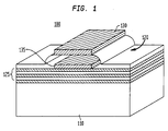
- FIG. 1 is a perspective schematic illustration of an acoustic resonator, which may be fabricated using the inventive method.
- the resonator 100 comprises a substrate 110, a film or layer 120 of piezoelectric material, and a means for retaining acoustic energy in the piezoelectric film, such as a Bragg reflecting region 125, between the substrate 110 and film 120.
- a layer of air may be used to suspend the film 120 above the substrate 110.
- a bottom electrode 135 and top electrode 130 are disposed on opposite surfaces of the piezoelectric film 120.
- the layer of piezoelectric material advantageously comprises A1N, but may be made of any suitable material that has piezoelectric qualities sufficient for the particular resonator application.
- Typical piezoelectric materials include, for example, quartz, zinc oxide (ZnO), and ceramic materials such as lithium niobate (LiNbO 3 ), lithium tantalate (LiTaO 3 ), paratellurite (TeO 2 ), and lead titanate zirconate (PZT).
- the substrate typically is comprised of silicon but may be fabricated with other materials such as quartz, sapphire, polysilicon, aerogel, and aluminum oxide (Al 2 O 3 ).
- the electrodes and particularly the bottom electrode 135 may comprise aluminum (Al) or a metal stack using titanium and Al. Besides use of Al and/or Ti/Al, other metals having a low sheet resistance and low surface roughness may be used for fabricating the electrodes 130, 135. Previous stacked metal electrodes often have comprised Ti/TiN/Al as the composition of choice.
- the inventive method is advantageous in that high-quality piezoelectric films can be fabricated when there is a decrease in the process window for depositing textured Ti-Al, and the quality of the piezoelectric film can be assured pre-fabrication, i.e ., before the piezoelectric film is deposited.
- This is accomplished by fabricating insulating layers 125 having a surface roughness that is sufficiently low to assure the high-quality piezoelectric film (e.g., ⁇ 10 ⁇ ), non-destructively evaluating these layers, and further smoothing them, if necessary.
- This method also reliably predicts the quality of the piezoelectric film before it is deposited.
- a process involving use of rotating magnet magnetrons and pulsed DC power supplies is applied to deposit the insulating layers and/or piezoelectric film.
- Rotating magnet magnetrons are used to provide film thickness uniformity, and such rotating magnet magnetrons are made possible in that process parameters are optimized to achieve a high deposition rate and correct index of refraction.
- the process comprises determination of a "cross-over point" such that the target will remain effective in emitting atoms and resisting the deposition of materials thereon.
- the "cross-over point” is defined as the point at which a pressure increase in the chamber 210 (see FIG. 2) becomes non-linear with the flow of reactive gasses, and is further defined below.
- the process makes use of the recognition that the quality of the piezoelectric film can be improved by addressing the surface roughness of the layers on which the piezoelectric film is deposited, i.e., providing an underlying insulating layer having a relatively smooth surface produces a higher quality piezoelectric film.
- the surface roughness of the insulating layers are monitored and smoothed, if necessary, before the piezoelectric film is deposited.
- the contemporaneously-filed Bower application described above (which is assigned to the present assignee and incorporated herein), describes the recognition that the surface roughness of the electrode underlying the piezoelectric film (FIG. 1, 135) affects the quality of the piezoelectric film 120.
- the Bower application thus describes a method of making a device having a piezoelectric film comprising controlling the surface roughness of the metal layer, which may include controlling the surface roughness of the insulating layers 125 underlying the metal layer 135.
- the Bower method comprises use of textured titanium (and a collimator in the deposition process), which increases the system tolerance or process window for surface roughness.
- the insulating layers 125 do not have to be as smooth as when the collimator is not used in order to achieve a high-quality piezoelectric film.
- the collimator also is known, however, for decreasing the thickness uniformity of the titanium layer.
- the insulating layers should be fabricated so they have root mean square (RMS) morphology reflecting a surface roughness of about less than 10 Angstroms.
- the RMS value reflects a true average, absolute value for the deviation or difference in the surface morphology from a mean value of zero, the value of zero reflecting a completely smooth surface.
- the RMS value is defined by the square root of the difference between the mean square and the square of the mean, or in other words, it is the normalized average value of the roughness relative to the median of the measured roughness.
- a "high-quality" piezoelectric film is defined herein as a film having a texture reflecting a good crystalline orientation of atoms, low stress (less than about 50 megaPascals ⁇ MPa ⁇ ), and appropriate index of refraction (approximately 2.0, more preferably 2.07 ⁇ 0.005, and more preferably 2.078 ⁇ . 0.005).
- Film thickness uniformity advantageously is 0.4% one Sigma, with a more preferred thickness uniformity of 0.2% one Sigma, with an even more preferred thickness uniformity of 0.1% three Sigma.
- the "quality" of a piezoelectric film as that term is used herein relates to at least one of the texture, stress, uniformity, and/or index of refraction of the piezoelectric film.
- “texture” as used herein is intended to describe the crystallographic alignment of grains in a polycrystalline film wherein "maximum texture” denotes a film having an alignment (orientation) of grains centered about a single direction at an angle subtended from (relative to) the growth direction.
- maximum texture denotes a film having an alignment (orientation) of grains centered about a single direction at an angle subtended from (relative to) the growth direction.
- the texture and thus quality of the piezoelectric film can be defined by reference to its "rocking curve.” More specifically, ideally crystallographic directions of the grains are centered about a single direction; as mentioned above, the performance of the piezoelectric film ( e . g . in a piezoelectric resonator), is dependent upon the crystalline orientation of the atoms comprising the film.
- the piezoelectric film advantageously is formed with a FWHM rocking curve of less than 3.5°, with a more preferred low rocking curve being less than about 2.5°, and more preferably less than 1.5° (FWHM).
- a high-quality piezoelectric film may be fabricated by applying a rotating magnetron and pulse DC reactive sputtering process to fabricate one or more layers of the piezoelectric device, including the insulating layers (FIG. 1, 125), and/or the piezoelectric film (FIG. 1, 120).
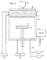
- FIG. 2 is a simplified, schematic representation of a rotating magnetron sputtering apparatus for use in depositing the piezoelectric 120, the insulating layers 125, and the electrodes 130, 135 on the substrate 110.
- the apparatus includes a chamber 210 (e.g ., a plasma chamber), and a pair of electrodes (the target 260 and anode ring 225) within the chamber.
- the electric potential applied to the electrodes may be controlled by a pulsed DC power source 230 or other suitable source.
- Various sources are provided for injecting gasses into the chamber.
- a first flow control source 240 injects noble gasses into the chamber (e.g ., Ar, Ze, and Kr), and a second flow control source 250 supplies a reactive gas (O 2 , N 2 , etc.) into the chamber 210.
- the gasses are supplied via gas delivery port 245.
- a target material is positioned within the sputtering chamber.
- the substrate 110 is also positioned therein, and disposed such that it is in communication with the target and gasses within the chamber.
- the target material 260 is mounted adjacent a rotating magnet assembly 280 which includes a magnet array to produce a magnetic field to penetrate the target material 260 and form an arc over its surface facing the substrate 110.
- a rotation motor 300 causes the rotating magnet assembly to rotate about an axis of rotation with respect to the target 260.
- the magnetic field generated across target 260 helps to confine free electrons near the surface of the target.
- the increased concentration of ions excited by these electrons at the target surface increases the efficiency of the sputtering process.
- the pressure within the chamber can be regulated with pressure regulators 240, 250 and throttle valve 270.
- An RF power supply 235 applies a bias voltage to the substrate platen 115 to control tensile film stress.
- a high-quality film may be achieved with this apparatus, and various parameters can be applied to optimize the processing conditions.
- Applicants have discovered a method comprising optimization of the reaction parameters to achieve a high-deposition rate and correct index of refraction.
- the method includes a step of determining the "cross-over point" in the process.
- the "cross-over point” is defined as the point at which a pressure increase in the chamber 210 becomes non-linear with the flow of reactive gasses, and this point reflects a reactive gas flow rate that strongly effects a reaction with the target material.
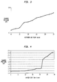
- FIG. 3 is a representative graph illustrating determination of the cross-over point in a process involving fabrication of an AlN piezoelectric film, in which the reactive gas comprises nitrogen and the target comprises aluminum.
- FIG. 4 is a representative graph illustrating determination of the cross-over point in a process involving fabrication of an SiO 2 layer, in which the reactive gas comprises oxygen and the target comprises silicon.
- the characteristic pressure-flow curve shows two asymptotic regimes.
- low flow of reactive gas to the left of the graph
- all the nitrogen is being reacted with metallic aluminum so introduction of small amounts of nitrogen does not increase the chamber pressure.
- gas flow is increased, gas is present in the chamber that cannot react with metal, and the unreacted gas causes an increase in pressure in the chamber.
- the target material becomes fully “poisoned” or coated with the reaction product (AlN) such that any further gas admitted into the chamber will not react with target material and will directly contribute to a pressure increase.
- the plot of pressure versus reactive gas flow shows a "crossover curve" from the behavior of a metallic target fully consuming reactive gas to the behavior of a fully poisoned target showing increasing pressure with further admission of reactive gas.
- FIG. 5 is a block diagram showing illustrative steps of one aspect of the invention.
- the invention comprises use of the cross-over curve in optimizing the reactive sputtering deposition process with use of rotating magnet magnetrons and pulsed DC power.
- the method includes a step of providing the target material within a sputtering chamber, with the target material being oriented on a rotating magnet assembly for producing a magnetic field across the target material.
- a substrate within the sputtering chamber in open communication with the target, and a pair of electrodes (target and anode ring) are positioned within the sputtering chamber.
- a suitable rotation speed is 282 rpms.
- the cross-over point for the flow of a reactive gas into the sputtering chamber is determined with appropriate settings to the pulse frequency and pulse width.
- the noble gas is introduced into the sputtering chamber, and then the reactive gas is added so that it reacts with a portion of the target material.
- the reactive gas is introduced incrementally into the sputtering chamber so that the flow rate of the reactive gas is maintained at a rate corresponding substantially to, but greater than, the flow rate at the cross-over point.
- a film is thus deposited on the substrate as the chamber is maintained just above the cross-over point.
- the cross-over point will result in a metallic film.
- the deposition rate decreases for at least 20 sccm and until the target is totally poisoned, becomes an insulator, and a plasma can no longer be maintained.
- a pulsed DC voltage is applied across the pair of electrodes (the target and anode ring) that are positioned within the sputtering chamber so that ions from the noble gas impinge upon the target material and eject atoms therefrom. Freed atoms of the target material react mostly at the target with the reactive gas to form a coating on the substrate. Maintaining the flow rate near the cross-over point is effective in optimizing the deposition conditions; the target will continue to be conductive while depositing a coating on the substrate, and poisoning of the target itself is controlled. Additionally, various other aspects of the process may be managed to improve the deposition rate and overall quality of the deposited films.
- the relevant parameters of the process may be monitored and adjusted, considering that the deposition rate is inversely proportional to the amount of reactive gas, the power supply pulse width, and the deposition pressure, and is directly proportional to the power.
- the deposition rate is unaffected by the power supply frequency.
- the index of refraction is inversely proportional to both the amount of reactive gas and the power supply pulse width.
- these deposition parameters may be adjusted to achieve an optimal deposition rate for producing substantially stress-free piezoelectric films having the desired index of refraction.
- the index of refraction of the deposited coating can be monitored and adjusted to achieve a desired index of refraction for the coating. This may comprise a coarse adjustment with reactive gas, followed by a fine tuning with pulse width.
- the current and/or voltage can be monitored and frequency adjusted to achieve a stable waveform.
- the pulse width of the DC voltage can be adjusted to improve the homogeneity of the film or coating formed on the substrate.
- the DC power can be increased or the pressure or flow rate reduced to improve the surface roughness for the film.
- the inventive process is advantageous for depositing piezoelectric films and also for optimizing the processing conditions for depositing the insulating layers, which will impact upon the texture of the piezoelectric films deposited thereon.
- additional parameters to consider are that a reduction in the surface roughness of the resultant SiO 2 films is achieved by increasing the power and/or decreasing the pressure.
- these parameters may be adjusted and optimized to achieve the highest deposition rate that produces films having the desired surface roughness and index of refraction. Applying this evaluative process, films may be consistently produced that have the desired index of refraction and a surface texture of less than 25 ⁇ (RMS), and more preferably less than 10. ⁇
- the surface roughness of the insulating layer may be measured and if necessary, further processed to achieve optimal quality piezoelectric films.
- the surface roughness of an SiO 2 film may be non-destructively measured by an Acoustic Force Microscope (AFM) located within the silicon laboratory in which the piezoelectric device is produced, e.g., a class 10 clean room where all silicon fabrication takes place or other Silicon Fabrication Research Laboratory (SFRL).
- AFM Acoustic Force Microscope
- SFRL Silicon Fabrication Research Laboratory
- a first step comprises determining the cross-over curve on a monitor wafer. This can be accomplished by arbitrarily setting the pulse frequency at 100 kHz and the pulse width at 25 nS.
- argon the noble gas
- a suitable flow rate for Ar is 20 sccm and a resultant chamber pressure of 1.5mTorr.
- the nitrogen is introduced incrementally (e.g. , in 1 sccm steps), as the voltage, current and chamber pressure are monitored to determine the flow rate that corresponds to the cross-over point. (Any one of the voltage, current, or chamber pressure plotted against flow rate will indicate the cross-over point; any one of these factors may be analyzed, or all three may be analyzed for confirmation.)
- Nitrogen the reactive gas
- the film is then deposited at a gas ratio approximately 3 sccm greater than the cross-over point.
- the stress and index of refraction of the deposited material are measured.
- the voltage-current of the magnetron should be monitored and if necessary, the frequency should be adjusted to achieve a stable waveform. The frequency does not affect the film quality and may be freely adjusted.
- the amount of reactive gas and power supply pulse width are adjusted to achieve the desired index of refraction.
- the gas ratios may be varied to make coarse corrections.
- the reverse-bias pulse width may be adjusted for fine-tuning correction of the index-the more the pulse width is increased (that is, the larger percentage of the selected frequency it covers), the higher the index will be, but increasing the pulse width also lowers the deposition rate.
- RF bias is applied to the substrate to control tensile stress.
- Monitor wafers are used to determine the bias that results in zero ⁇ fifty MPa stress when the index is fine tuned. The system should be monitored and corrected for zero stress when the index is fine-tuned.
- the pulsed DC power may be adjusted as described in the above-referenced Miller application, incorporated herein, to enhance the desired film constituency, stress, and texture through more efficient reaction by the reactive gasses. Each power change requires re-optimization of the index of refraction and stress.
- a silicon dioxide (SiO 2 ) film may be fabricated using a silicon target doped with ⁇ 2% boron. Oxygen is used as the reactive gas to oxidize the silicon target and form the SiO 2 .
- a first step in the insulating layer deposition comprises determining the cross-over point on a monitor wafer.
- the initial pulse frequency is arbitrarily set at 100 kHz, the pulse width at 25 nS, and the argon flow adjusted to 30 sccm.
- Oxygen gas is added in 1 sccm steps while the voltage, current and chamber pressure are recorded. The flow rate is maintained at a gas ratio of approximately 3 sccm greater than the cross-over point.
- a film is deposited onto a new monitor wafer and the index is measured.
- Stress is ⁇ 125MPa ( ⁇ 25MPa) compressive and cannot be corrected using RF bias or chamber pressure. Accordingly, the stress level may be addressed by controlling the A1N stress ( i . e . leaving AlN at 100 MPa tensile stress).
- the voltage-current of the magnetron should be monitored and if necessary, the frequency should be adjusted to achieve a stable waveform. The frequency does not affect the film quality and may be freely adjusted.
- the amount of reactive gas and power supply pulse width are adjusted to achieve the desired index of refraction.
- the gas ratios may be varied to make coarse corrections.
- the reverse-bias pulse width may be adjusted for fine-tuning correction of the index-the more the pulse width is increased (that is, the larger percentage of the selected frequency it covers), the higher the index will be, but increasing the pulse width also lowers the deposition rate.
- the surface roughness is measured and the power and pressure adjusted until the desired surface roughness is achieved; the surface roughness of the resultant SiO 2 film improves with increasing power and decreasing pressure.
- a deposition power of 2kW and a 30/28 sccm Ar/ O 2 ratio should result in a film having a surface roughness of less than 15 ⁇ (RMS).
- a surface roughness of 15 ⁇ can be improved to less than 10 ⁇ using the HSE.
- Roughness greater than 20 ⁇ needs CMP to improve to less than 10 ⁇ .
- An advantageous aspect of the invention comprises the ability to measure the SiO 2 surface morphology and improve this surface to less than 10 ⁇ prior to the deposition of the piezoelectric layer, which reduces the cost of piezoelectric film fabrication.
Landscapes
- Chemical & Material Sciences (AREA)
- Engineering & Computer Science (AREA)
- Chemical Kinetics & Catalysis (AREA)
- Materials Engineering (AREA)
- Mechanical Engineering (AREA)
- Metallurgy (AREA)
- Organic Chemistry (AREA)
- Manufacturing & Machinery (AREA)
- Physical Vapour Deposition (AREA)
- Formation Of Insulating Films (AREA)
Abstract
Description
Claims (17)
- A method for use in fabricating a piezoelectric film deposited on at least one insulating layer comprising determining the surface roughness of the at least one insulating layer and achieving a surface roughness for the insulating layer that is sufficiently low that the quality of the piezoelectric film can be determined prior to fabrication of the piezoelectric film.
- The method of claim 1 in which at least one metal layer is deposited between the insulating layer and the piezoelectric film.
- The method of claim 1 comprising a reactive sputtering process using rotating magnet magnetrons and pulsed DC power in depositing the at least one insulating layer for promoting the thickness uniformity of the at least one insulating layer.
- The method of claim 1 comprising a reactive sputtering process using rotating magnet magnetrons and pulsed DC power in depositing the piezoelectric film for promoting the thickness uniformity of the piezoelectric film.
- The method of claim 1 comprising a reactive sputtering process in which a target material and a substrate are disposed within a sputtering chamber and a reactive gas is introduced into the chamber, wherein the process further comprises the steps of:determining the cross-over point for the flow of a reactive gas into the sputtering chamber; andintroducing a reactive gas into the sputtering chamber, wherein the reactive gas reacts with a portion of said target material, the reactive gas being introduced into the sputtering chamber at a flow rate corresponding substantially to the flow rate at the cross-over point.
- The method of claim 1 comprising the steps of measuring the surface roughness of the at least one insulating layer before the piezoelectric film is deposited and achieving a desired surface roughness for the at least one insulating layer of less than 10(RMS).

- The method of claim 6 in which the surface roughness of the at least one insulating layer is non-destructively measured in situ by an acoustic force microscope.
- The method of claim 6 in which the desired surface roughness is achieved with use of chemical mechanical polishing or a hydrogen hot sputter etch process.
- A method of reactive sputtering with rotating magnetrons and pulsed DC power, the method comprising:providing a target material within a sputtering chamber, the target material being oriented on a rotating magnet assembly;positioning a substrate within the sputtering chamber;causing the magnet assembly to rotate for producing a magnetic field across the target material;introducing a noble gas into the sputtering chamber,introducing a reactive gas into the sputtering chamber, wherein the reactive gas reacts with a portion of said target material; andapplying a pulsed DC voltage across a pair of electrodes that are positioned within the sputtering chamber so that ions from the noble gas impinge upon the target material and eject atoms therefrom, wherein the freed atoms of the target material react with the reactive gas to form a coating on the substrate.
- The method of claim 9 further comprising the steps of determining the cross-over point for the flow of the reactive gas into the sputtering chamber and introducing the reactive gas into the sputtering chamber at a flow rate corresponding substantially to the flow rate at the cross-over point.
- The method of claim 9 wherein the pair of electrodes comprise a target and anode ring.
- The method of claim 9 further comprising a step of adjusting the pulse width of the DC voltage to improve the structure of the coating formed on the substrate.
- The method of claim 9 further comprising a step of monitoring the index of refraction of the coating formed on the substrate and the current or power supply pulse width to achieve a desired index of refraction for the coating.
- The method of claim 9 further comprising at least one of a step of at least one of increasing the pulsed DC voltage or reducing the pressure to achieve a desired surface roughness for the coating.
- The method of claim 9 further comprising a step of monitoring at least one of the current or pulsed DC voltage and adjusting the frequency to achieve a stable waveform.
- The method of claim 9 comprising at least one of (i) deposition of one or more insulating layers on a substrate; and (ii) deposition of a piezoelectric film on at least one of an insulating layer or a metal layer, (iii) in the fabrication of a piezoelectric device.
- A method for fabricating a piezoelectric device comprising non-destructively predicting and assuring the quality of a piezoelectric film to be deposited on at least one insulating layer by achieving a surface roughness for the insulating layer that is approximately less than 10 Angstroms RMS.
Applications Claiming Priority (2)
| Application Number | Priority Date | Filing Date | Title |
|---|---|---|---|
| US503225 | 1990-04-02 | ||
| US09/503,225 US6342134B1 (en) | 2000-02-11 | 2000-02-11 | Method for producing piezoelectric films with rotating magnetron sputtering system |
Publications (3)
| Publication Number | Publication Date |
|---|---|
| EP1124270A2 true EP1124270A2 (en) | 2001-08-16 |
| EP1124270A3 EP1124270A3 (en) | 2005-09-14 |
| EP1124270B1 EP1124270B1 (en) | 2011-05-11 |
Family
ID=24001226
Family Applications (1)
| Application Number | Title | Priority Date | Filing Date |
|---|---|---|---|
| EP01300748A Expired - Lifetime EP1124270B1 (en) | 2000-02-11 | 2001-01-29 | Method for producing piezoelectric films with rotating magnetron sputtering system |
Country Status (4)
| Country | Link |
|---|---|
| US (1) | US6342134B1 (en) |
| EP (1) | EP1124270B1 (en) |
| JP (1) | JP5093943B2 (en) |
| KR (2) | KR100860182B1 (en) |
Cited By (5)
| Publication number | Priority date | Publication date | Assignee | Title |
|---|---|---|---|---|
| WO2006064414A1 (en) * | 2004-12-15 | 2006-06-22 | Philips Intellectual Property & Standards Gmbh | Thin film acoustic reflector stack |
| CN100498659C (en) * | 2006-12-29 | 2009-06-10 | 中国电信股份有限公司 | Method and apparatus for providing mouse function for remote controller |
| WO2021148195A1 (en) * | 2020-01-24 | 2021-07-29 | Evatec Ag | Phase shift controlled sputter system and process |
| CN115863489A (en) * | 2023-03-02 | 2023-03-28 | 广东联塑班皓新能源科技集团有限公司 | Photovoltaic module manufacturing method |
| CN119144930A (en) * | 2024-11-15 | 2024-12-17 | 武汉大学 | High-purity light metal doped LiNbO3Piezoelectric coating and preparation method thereof |
Families Citing this family (45)
| Publication number | Priority date | Publication date | Assignee | Title |
|---|---|---|---|---|
| US6329305B1 (en) * | 2000-02-11 | 2001-12-11 | Agere Systems Guardian Corp. | Method for producing devices having piezoelectric films |
| JP2005236337A (en) * | 2001-05-11 | 2005-09-02 | Ube Ind Ltd | Thin film acoustic resonator and manufacturing method thereof |
| GB0116688D0 (en) * | 2001-07-07 | 2001-08-29 | Trikon Holdings Ltd | Method of depositing aluminium nitride |
| JP2003121133A (en) * | 2001-10-17 | 2003-04-23 | Acbtec:Kk | Method and apparatus for forming multilayer thin film |
| US6906451B2 (en) | 2002-01-08 | 2005-06-14 | Murata Manufacturing Co., Ltd. | Piezoelectric resonator, piezoelectric filter, duplexer, communication apparatus, and method for manufacturing piezoelectric resonator |
| JP2004221622A (en) * | 2002-01-08 | 2004-08-05 | Murata Mfg Co Ltd | Piezoelectric resonator, piezoelectric filter, duplexer, communication apparatus, and manufacturing method of piezoelectric resonator |
| JP2004048639A (en) * | 2002-05-17 | 2004-02-12 | Murata Mfg Co Ltd | Piezoelectric resonator and manufacturing method thereof |
| JP3846406B2 (en) | 2002-01-10 | 2006-11-15 | 株式会社村田製作所 | Electronic component, manufacturing method thereof, filter and duplexer using the same, and electronic communication device |
| US7091412B2 (en) * | 2002-03-04 | 2006-08-15 | Nanoset, Llc | Magnetically shielded assembly |
| US20040210289A1 (en) * | 2002-03-04 | 2004-10-21 | Xingwu Wang | Novel nanomagnetic particles |
| US7162302B2 (en) * | 2002-03-04 | 2007-01-09 | Nanoset Llc | Magnetically shielded assembly |
| US20040225213A1 (en) * | 2002-01-22 | 2004-11-11 | Xingwu Wang | Magnetic resonance imaging coated assembly |
| US20050260331A1 (en) * | 2002-01-22 | 2005-11-24 | Xingwu Wang | Process for coating a substrate |
| US6617178B1 (en) * | 2002-07-02 | 2003-09-09 | Agilent Technologies, Inc | Test system for ferroelectric materials and noble metal electrodes in semiconductor capacitors |
| DE10301261B4 (en) * | 2003-01-15 | 2018-03-22 | Snaptrack, Inc. | Bulk acoustic wave device and method of manufacture |
| US20050155779A1 (en) * | 2003-04-08 | 2005-07-21 | Xingwu Wang | Coated substrate assembly |
| US20050149169A1 (en) * | 2003-04-08 | 2005-07-07 | Xingwu Wang | Implantable medical device |
| US20050278020A1 (en) * | 2003-04-08 | 2005-12-15 | Xingwu Wang | Medical device |
| US20050240100A1 (en) * | 2003-04-08 | 2005-10-27 | Xingwu Wang | MRI imageable medical device |
| US20070010702A1 (en) * | 2003-04-08 | 2007-01-11 | Xingwu Wang | Medical device with low magnetic susceptibility |
| US20050244337A1 (en) * | 2003-04-08 | 2005-11-03 | Xingwu Wang | Medical device with a marker |
| US20060102871A1 (en) * | 2003-04-08 | 2006-05-18 | Xingwu Wang | Novel composition |
| US20050261763A1 (en) * | 2003-04-08 | 2005-11-24 | Xingwu Wang | Medical device |
| US20050119725A1 (en) * | 2003-04-08 | 2005-06-02 | Xingwu Wang | Energetically controlled delivery of biologically active material from an implanted medical device |
| US20050149002A1 (en) * | 2003-04-08 | 2005-07-07 | Xingwu Wang | Markers for visualizing interventional medical devices |
| GB0308249D0 (en) * | 2003-04-10 | 2003-05-14 | Trikon Technologies Ltd | Method of depositing piezoelectric films |
| US20070027532A1 (en) * | 2003-12-22 | 2007-02-01 | Xingwu Wang | Medical device |
| JP4737375B2 (en) * | 2004-03-11 | 2011-07-27 | セイコーエプソン株式会社 | Method for manufacturing actuator device, method for manufacturing liquid jet head, and method for manufacturing liquid jet device |
| US7565723B2 (en) * | 2004-03-30 | 2009-07-28 | Brother Kogyo Kabushik Kaisha | Piezoelectric actuator and method of fabricating piezoelectric actuator |
| US20060118758A1 (en) * | 2004-09-15 | 2006-06-08 | Xingwu Wang | Material to enable magnetic resonance imaging of implantable medical devices |
| JP4379475B2 (en) * | 2004-12-24 | 2009-12-09 | 株式会社村田製作所 | Piezoelectric thin film resonator and manufacturing method thereof |
| US20060140867A1 (en) * | 2004-12-28 | 2006-06-29 | Helfer Jeffrey L | Coated stent assembly and coating materials |
| DE102006061324B4 (en) * | 2006-06-20 | 2008-07-24 | Fraunhofer-Gesellschaft zur Förderung der angewandten Forschung e.V. | A method of controlling a high power reactive pulse magnetron sputtering process and apparatus therefor |
| FR2951026B1 (en) * | 2009-10-01 | 2011-12-02 | St Microelectronics Sa | METHOD FOR MANUFACTURING BAW RESONATORS ON A SEMICONDUCTOR WAFER |
| FR2951023B1 (en) * | 2009-10-01 | 2012-03-09 | St Microelectronics Sa | METHOD FOR MANUFACTURING MONOLITHIC OSCILLATORS WITH BAW RESONATORS |
| FR2951024B1 (en) * | 2009-10-01 | 2012-03-23 | St Microelectronics Sa | METHOD FOR MANUFACTURING BAW RESONATOR WITH HIGH QUALITY FACTOR |
| JP5855410B2 (en) * | 2011-09-29 | 2016-02-09 | 株式会社アルバック | Method for forming aluminum nitride film |
| WO2013070679A1 (en) * | 2011-11-08 | 2013-05-16 | Tosoh Smd, Inc. | Silicon sputtering target with special surface treatment and good particle performance and methods of making the same |
| DE102013213935B4 (en) * | 2013-07-16 | 2015-08-20 | Fraunhofer-Gesellschaft zur Förderung der angewandten Forschung e.V. | Method for depositing a piezoelectric AlN-containing layer |
| GB201505578D0 (en) * | 2015-03-31 | 2015-05-13 | Spts Technologies Ltd | Method and apparatus for depositing a material |
| GB201706284D0 (en) * | 2017-04-20 | 2017-06-07 | Spts Technologies Ltd | A method and apparatus for controlling stress variation in a material layer formed via pulsed DC physical vapour deposition |
| GB201714646D0 (en) * | 2017-09-12 | 2017-10-25 | Spts Technologies Ltd | Saw device and method of manufacture |
| WO2021146917A1 (en) * | 2020-01-21 | 2021-07-29 | 济南晶正电子科技有限公司 | Piezoelectric thin film composite substrate and manufacturing method therefor |
| CN114389555A (en) * | 2020-10-21 | 2022-04-22 | 诺思(天津)微系统有限责任公司 | Bulk acoustic wave resonator, method of manufacturing the same, filter, and electronic apparatus |
| JP2023029041A (en) * | 2021-08-20 | 2023-03-03 | 株式会社レゾナック | Manufacturing method for laminated body |
Family Cites Families (20)
| Publication number | Priority date | Publication date | Assignee | Title |
|---|---|---|---|---|
| EP0117258B1 (en) * | 1983-02-23 | 1987-05-20 | Ibm Deutschland Gmbh | Process for the production of metallic layers adhering to plastic supports |
| JPH04176866A (en) * | 1990-11-08 | 1992-06-24 | Showa Shinku:Kk | Film forming velocity controlling device for sputtering equipment |
| JPH06244261A (en) * | 1990-12-31 | 1994-09-02 | Texas Instr Inc <Ti> | Semiconductor device manufacturing process control sensor |
| US5319977A (en) * | 1991-06-20 | 1994-06-14 | The Board Of Trustees Of The Leland Stanford Junior University | Near field acoustic ultrasonic microscope system and method |
| CA2123479C (en) * | 1993-07-01 | 1999-07-06 | Peter A. Sieck | Anode structure for magnetron sputtering systems |
| US5378341A (en) | 1993-10-13 | 1995-01-03 | The United States Of America As Represented By The Secretary Of The Air Force | Conical magnetron sputter source |
| EP0669412B1 (en) * | 1994-02-25 | 2002-05-22 | Sumitomo Electric Industries, Ltd. | Aluminim nitride thin film substrate and process for producing same |
| JPH07243039A (en) * | 1994-03-02 | 1995-09-19 | Chugai Ro Co Ltd | DC magnetron type reactive sputtering method |
| US5651865A (en) * | 1994-06-17 | 1997-07-29 | Eni | Preferential sputtering of insulators from conductive targets |
| US5693197A (en) | 1994-10-06 | 1997-12-02 | Hmt Technology Corporation | DC magnetron sputtering method and apparatus |
| JPH0949077A (en) * | 1995-08-09 | 1997-02-18 | Ulvac Japan Ltd | DC sputtering equipment |
| US5702573A (en) * | 1996-01-29 | 1997-12-30 | Varian Associates, Inc. | Method and apparatus for improved low pressure collimated magnetron sputter deposition of metal films |
| JPH09302469A (en) * | 1996-05-09 | 1997-11-25 | Asahi Glass Co Ltd | Sputtering method |
| KR980011943A (en) * | 1996-07-24 | 1998-04-30 | 김광호 | Sputtering for large diameter wafers |
| US5830327A (en) | 1996-10-02 | 1998-11-03 | Intevac, Inc. | Methods and apparatus for sputtering with rotating magnet sputter sources |
| US5935641A (en) * | 1996-10-23 | 1999-08-10 | Texas Instruments Incorporated | Method of forming a piezoelectric layer with improved texture |
| JP3813740B2 (en) * | 1997-07-11 | 2006-08-23 | Tdk株式会社 | Substrates for electronic devices |
| EP0968318A1 (en) * | 1997-11-24 | 2000-01-05 | CVC, Inc. | Pulsed mode deposition for low rate film deposition |
| US6001227A (en) | 1997-11-26 | 1999-12-14 | Applied Materials, Inc. | Target for use in magnetron sputtering of aluminum for forming metallization films having low defect densities and methods for manufacturing and using such target |
| US6060818A (en) * | 1998-06-02 | 2000-05-09 | Hewlett-Packard Company | SBAR structures and method of fabrication of SBAR.FBAR film processing techniques for the manufacturing of SBAR/BAR filters |
-
2000
- 2000-02-11 US US09/503,225 patent/US6342134B1/en not_active Expired - Lifetime
-
2001
- 2001-01-29 EP EP01300748A patent/EP1124270B1/en not_active Expired - Lifetime
- 2001-02-09 KR KR1020010006412A patent/KR100860182B1/en not_active Expired - Lifetime
- 2001-02-09 JP JP2001033034A patent/JP5093943B2/en not_active Expired - Lifetime
-
2007
- 2007-07-23 KR KR1020070073750A patent/KR100890080B1/en not_active Expired - Fee Related
Cited By (7)
| Publication number | Priority date | Publication date | Assignee | Title |
|---|---|---|---|---|
| WO2006064414A1 (en) * | 2004-12-15 | 2006-06-22 | Philips Intellectual Property & Standards Gmbh | Thin film acoustic reflector stack |
| CN100557963C (en) * | 2004-12-15 | 2009-11-04 | Nxp股份有限公司 | Thin film acoustic reflector lamination, manufacturing method and configuration |
| CN100498659C (en) * | 2006-12-29 | 2009-06-10 | 中国电信股份有限公司 | Method and apparatus for providing mouse function for remote controller |
| WO2021148195A1 (en) * | 2020-01-24 | 2021-07-29 | Evatec Ag | Phase shift controlled sputter system and process |
| CN115863489A (en) * | 2023-03-02 | 2023-03-28 | 广东联塑班皓新能源科技集团有限公司 | Photovoltaic module manufacturing method |
| CN115863489B (en) * | 2023-03-02 | 2023-06-30 | 广东联塑班皓新能源科技集团有限公司 | Manufacturing method of photovoltaic module |
| CN119144930A (en) * | 2024-11-15 | 2024-12-17 | 武汉大学 | High-purity light metal doped LiNbO3Piezoelectric coating and preparation method thereof |
Also Published As
| Publication number | Publication date |
|---|---|
| JP5093943B2 (en) | 2012-12-12 |
| US6342134B1 (en) | 2002-01-29 |
| KR100890080B1 (en) | 2009-03-24 |
| KR20070092693A (en) | 2007-09-13 |
| EP1124270B1 (en) | 2011-05-11 |
| EP1124270A3 (en) | 2005-09-14 |
| KR100860182B1 (en) | 2008-09-24 |
| KR20010082101A (en) | 2001-08-29 |
| JP2001279438A (en) | 2001-10-10 |
Similar Documents
| Publication | Publication Date | Title |
|---|---|---|
| EP1124270B1 (en) | Method for producing piezoelectric films with rotating magnetron sputtering system | |
| US6329305B1 (en) | Method for producing devices having piezoelectric films | |
| Iriarte et al. | Reactive sputter deposition of highly oriented AlN films at room temperature | |
| US20090246385A1 (en) | Control of crystal orientation and stress in sputter deposited thin films | |
| Shao et al. | High quality co-sputtering AlScN thin films for piezoelectric Lamb-wave resonators | |
| US4640756A (en) | Method of making a piezoelectric shear wave resonator | |
| US6312568B2 (en) | Two-step AIN-PVD for improved film properties | |
| Engelmark et al. | Synthesis of highly oriented piezoelectric AlN films by reactive sputter deposition | |
| KR102931304B1 (en) | Piezoelectric bulk layer with tilted C-axis orientation and method for manufacturing the same | |
| EP1174525B1 (en) | Thin film, method for manufacturing thin film, and electronic component | |
| US7010837B2 (en) | Method for manufacturing an electronic component | |
| US11824511B2 (en) | Method for manufacturing piezoelectric bulk layers with tilted c-axis orientation | |
| US12029129B2 (en) | Method and apparatus for tuning film properties during thin film deposition | |
| KR20030037223A (en) | Method of Depositing Aluminium Nitride | |
| KR20220036855A (en) | A METHOD OF DEPOSITING LOW DEFECT Al1-xScxN FILMS | |
| Clement et al. | Effects of post-deposition vacuum annealing on the piezoelectric properties of AlScN thin films sputtered on 200 mm production wafers | |
| EP3454470B1 (en) | Method of manufacture of a surface acoustic wave device and surface acoustic wave device | |
| CN119433480B (en) | Process debugging method for preparing thin films by reactive magnetron sputtering | |
| Mishin et al. | Optimizing high concentration scandium aluminum nitride films | |
| US6153268A (en) | Method for producing oriented piezoelectric films | |
| US6746577B1 (en) | Method and apparatus for thickness control and reproducibility of dielectric film deposition | |
| Chang et al. | Characterization of lead zirconate titanate thin film deposition onto Pt/Ti/SiO2/Si substrates | |
| Mishin | Improving manufacturability of bulk acoustic wave and surface acoustic wave devices | |
| Mazzalai et al. | Developing production process for high performance piezoelectrics in MEMS applications | |
| KR20240156413A (en) | POI(piezoelectric-on-insulator) substrate and process for producing POI(piezoelectric-on-insulator) substrate |
Legal Events
| Date | Code | Title | Description |
|---|---|---|---|
| PUAI | Public reference made under article 153(3) epc to a published international application that has entered the european phase |
Free format text: ORIGINAL CODE: 0009012 |
|
| AK | Designated contracting states |
Kind code of ref document: A2 Designated state(s): AT BE CH CY DE DK ES FI FR GB GR IE IT LI LU MC NL PT SE TR |
|
| AX | Request for extension of the european patent |
Free format text: AL;LT;LV;MK;RO;SI |
|
| RIC1 | Information provided on ipc code assigned before grant |
Ipc: 7H 01L 41/22 A Ipc: 7C 23C 14/35 B |
|
| PUAL | Search report despatched |
Free format text: ORIGINAL CODE: 0009013 |
|
| AK | Designated contracting states |
Kind code of ref document: A3 Designated state(s): AT BE CH CY DE DK ES FI FR GB GR IE IT LI LU MC NL PT SE TR |
|
| AX | Request for extension of the european patent |
Extension state: AL LT LV MK RO SI |
|
| 17P | Request for examination filed |
Effective date: 20060314 |
|
| AKX | Designation fees paid |
Designated state(s): DE FR GB |
|
| RAP3 | Party data changed (applicant data changed or rights of an application transferred) |
Owner name: LUCENT TECHNOLOGIES INC. |
|
| GRAP | Despatch of communication of intention to grant a patent |
Free format text: ORIGINAL CODE: EPIDOSNIGR1 |
|
| GRAS | Grant fee paid |
Free format text: ORIGINAL CODE: EPIDOSNIGR3 |
|
| GRAA | (expected) grant |
Free format text: ORIGINAL CODE: 0009210 |
|
| AK | Designated contracting states |
Kind code of ref document: B1 Designated state(s): DE FR GB |
|
| REG | Reference to a national code |
Ref country code: GB Ref legal event code: FG4D |
|
| REG | Reference to a national code |
Ref country code: DE Ref legal event code: R096 Ref document number: 60144587 Country of ref document: DE Effective date: 20110622 |
|
| PLBE | No opposition filed within time limit |
Free format text: ORIGINAL CODE: 0009261 |
|
| STAA | Information on the status of an ep patent application or granted ep patent |
Free format text: STATUS: NO OPPOSITION FILED WITHIN TIME LIMIT |
|
| 26N | No opposition filed |
Effective date: 20120214 |
|
| REG | Reference to a national code |
Ref country code: DE Ref legal event code: R097 Ref document number: 60144587 Country of ref document: DE Effective date: 20120214 |
|
| PGFP | Annual fee paid to national office [announced via postgrant information from national office to epo] |
Ref country code: FR Payment date: 20140108 Year of fee payment: 14 |
|
| REG | Reference to a national code |
Ref country code: FR Ref legal event code: ST Effective date: 20150930 |
|
| PG25 | Lapsed in a contracting state [announced via postgrant information from national office to epo] |
Ref country code: FR Free format text: LAPSE BECAUSE OF NON-PAYMENT OF DUE FEES Effective date: 20150202 |
|
| PGFP | Annual fee paid to national office [announced via postgrant information from national office to epo] |
Ref country code: GB Payment date: 20151224 Year of fee payment: 16 |
|
| GBPC | Gb: european patent ceased through non-payment of renewal fee |
Effective date: 20170129 |
|
| PG25 | Lapsed in a contracting state [announced via postgrant information from national office to epo] |
Ref country code: GB Free format text: LAPSE BECAUSE OF NON-PAYMENT OF DUE FEES Effective date: 20170129 |
|
| REG | Reference to a national code |
Ref country code: DE Ref legal event code: R082 Ref document number: 60144587 Country of ref document: DE Representative=s name: DILG, HAEUSLER, SCHINDELMANN PATENTANWALTSGESE, DE Ref country code: DE Ref legal event code: R082 Ref document number: 60144587 Country of ref document: DE Representative=s name: DILG HAEUSLER SCHINDELMANN PATENTANWALTSGESELL, DE Ref country code: DE Ref legal event code: R081 Ref document number: 60144587 Country of ref document: DE Owner name: AVAGO TECHNOLOGIES GENERAL IP (SINGAPORE) PTE., SG Free format text: FORMER OWNER: LUCENT TECHNOLOGIES INC., MURRAY HILL, N.J., US |
|
| PGFP | Annual fee paid to national office [announced via postgrant information from national office to epo] |
Ref country code: DE Payment date: 20191218 Year of fee payment: 20 |
|
| REG | Reference to a national code |
Ref country code: DE Ref legal event code: R071 Ref document number: 60144587 Country of ref document: DE |