EP1124260A2 - Semiconductor device with reverse conducting faculty - Google Patents
Semiconductor device with reverse conducting faculty Download PDFInfo
- Publication number
- EP1124260A2 EP1124260A2 EP01301067A EP01301067A EP1124260A2 EP 1124260 A2 EP1124260 A2 EP 1124260A2 EP 01301067 A EP01301067 A EP 01301067A EP 01301067 A EP01301067 A EP 01301067A EP 1124260 A2 EP1124260 A2 EP 1124260A2
- Authority
- EP
- European Patent Office
- Prior art keywords
- region
- diodes
- anode
- cathode
- semiconductor device
- Prior art date
- Legal status (The legal status is an assumption and is not a legal conclusion. Google has not performed a legal analysis and makes no representation as to the accuracy of the status listed.)
- Withdrawn
Links
- 239000004065 semiconductor Substances 0.000 title claims abstract description 92
- 230000002441 reversible effect Effects 0.000 title claims abstract description 67
- 230000006698 induction Effects 0.000 claims abstract description 72
- 230000003068 static effect Effects 0.000 claims abstract description 72
- 239000000758 substrate Substances 0.000 claims abstract description 56
- 230000015556 catabolic process Effects 0.000 claims abstract description 48
- 230000000670 limiting effect Effects 0.000 claims description 12
- 230000003247 decreasing effect Effects 0.000 claims description 3
- 229910052710 silicon Inorganic materials 0.000 abstract description 17
- 239000010703 silicon Substances 0.000 abstract description 17
- XUIMIQQOPSSXEZ-UHFFFAOYSA-N Silicon Chemical compound [Si] XUIMIQQOPSSXEZ-UHFFFAOYSA-N 0.000 abstract description 12
- 238000011084 recovery Methods 0.000 description 16
- 239000003990 capacitor Substances 0.000 description 13
- 238000010586 diagram Methods 0.000 description 6
- 238000000926 separation method Methods 0.000 description 6
- 239000000969 carrier Substances 0.000 description 2
- 238000000034 method Methods 0.000 description 2
- 230000002829 reductive effect Effects 0.000 description 2
- 230000001052 transient effect Effects 0.000 description 2
- VYPSYNLAJGMNEJ-UHFFFAOYSA-N Silicium dioxide Chemical compound O=[Si]=O VYPSYNLAJGMNEJ-UHFFFAOYSA-N 0.000 description 1
- 230000002159 abnormal effect Effects 0.000 description 1
- 239000004020 conductor Substances 0.000 description 1
- 238000007599 discharging Methods 0.000 description 1
- 238000004519 manufacturing process Methods 0.000 description 1
- 238000012986 modification Methods 0.000 description 1
- 230000004048 modification Effects 0.000 description 1
- 229910052814 silicon oxide Inorganic materials 0.000 description 1
Images


Classifications
-
- H—ELECTRICITY
- H10—SEMICONDUCTOR DEVICES; ELECTRIC SOLID-STATE DEVICES NOT OTHERWISE PROVIDED FOR
- H10D—INORGANIC ELECTRIC SEMICONDUCTOR DEVICES
- H10D84/00—Integrated devices formed in or on semiconductor substrates that comprise only semiconducting layers, e.g. on Si wafers or on GaAs-on-Si wafers
- H10D84/60—Integrated devices formed in or on semiconductor substrates that comprise only semiconducting layers, e.g. on Si wafers or on GaAs-on-Si wafers characterised by the integration of at least one component covered by groups H10D10/00 or H10D18/00, e.g. integration of BJTs
- H10D84/676—Combinations of only thyristors
Definitions
- the present invention relates to a semiconductor device, and more particularly to a semiconductor device having reverse conducting faculty comprising a switching element including a semiconductor substrate of a first conductivity type having first and second major surfaces, a first main electrode region of the first conductivity type formed on the first major surface of the semiconductor substrate, a second major electrode region of a second conductivity type formed on the second surface of the semiconductor substrate, and a control electrode region of the second conductivity type for controlling a current passing between the first and second main electrode regions.
- a switching element including a semiconductor substrate of a first conductivity type having first and second major surfaces, a first main electrode region of the first conductivity type formed on the first major surface of the semiconductor substrate, a second major electrode region of a second conductivity type formed on the second surface of the semiconductor substrate, and a control electrode region of the second conductivity type for controlling a current passing between the first and second main electrode regions.
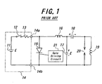
- FIG. 1 shows an example of a known pulse generating circuit used as a voltage supply source for use in a pulse laser.
- a pulse generating circuit between output terminals 14a and 14b of a charging circuit 14 including a DC power supply source 11, a switch 12 and a current limiting resistor 13, is connected a static induction thyristor 15 (herein after abbreviated as SIThy).
- SIThy static induction thyristor 15
- resonance coil 16 and capacitor 17 in parallel with the capacitor 17 are connected a capacitor 18 and a coil 19 having a large inductance, and a discharge gap 20 is connected across the coil 19 as a load.
- the switch 12 Under a non-conductive condition of the SIThy 15, at first the switch 12 is closed to charge the capacitor 17 through the resistor 13 and coil 16. During this charging process, an impedance of the coil 19 at a lower frequency is low, and thus the capacitor 18 is also charged through the coil 19. Now an output voltage of the DC power supply source 11 is denoted by E. After charging the capacitors 17 and 18 up to E, the SIThy 15 is turned-on by means of a gate driving circuit 21. Then, charge stored in the capacitor 17 is discharged through the SIThy 15 in accordance with a resonance characteristic determined by the coil 16 and capacitor 17, and the capacitor 17 is charged in a reverse polarity to a polarity in which the capacitor 17 is charged up to substantially -E.
- Charge stored in the capacitor 18 is also discharged through the SIThy 15 and coil 19. Since an impedance of the coil 19 is very high for a high frequency, the discharge is conducted very slowly. Therefore, a voltage of about - 2E will be applied across the discharge gap 20. When a discharge occurs, charge stored in the capacitors 17 and 18 disappears by discharge at the discharge gap 20. And the switch 12 is closed to initiate the charging operation again.
- Fig. 3 is a graph showing a voltage across the anode-cathode path of the SIThy 15. When discharge does not occurs correctly, a reverse voltage is applied to the SIThy 15. In this case, a reverse current flows from the cathode to the gate of the SIThy 15, and this results in application of an excessive high reverse voltage like as a reverse recovery phenomenon of the diode.
- the static induction thyristor having such a diode is generally called a reverse conducting static induction thyristor.
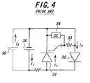
- Fig. 4 is an equivalent circuit of the above mentioned reverse conducting static induction thyristor.
- a diode 32 is connected in anti-parallel with a static induction thyristor (SIThy) 31 such that an anode of the diode is connected to a cathode of the SIThy and a cathode of the diode is connected to an anode of the SIThy.
- the anode of the diode 32 is further connected to a gate of the SIThy 31 by means of a resistor 33, and the gate of the SIThy is connected to a gate driving circuit (GC) 34 which controls the turn-on/turn-off of the SIThy.
- GC gate driving circuit
- a current I T flows through the SIThy
- a voltage supply source 36 is connected in a reverse polarity as depicted by a broken line in Fig. 4
- a current I R flows through the diode 32 to protect the SIThy 31 from being breakdown.
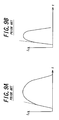
- Fig. 5 is a cross sectional view showing the structure of the above mentioned known reverse conducting static induction thyristor.
- a p + gate regions 43 In one major surface of an n - silicon substrate 41 there is formed a p + gate regions 43, and p + buried gate regions 44 are formed within a channel region.
- a gate electrode 45 is provided on the gate region 42 via a conductive layer 45a.
- the buried gate regions 43 are formed as a comb shape to be surrounded by the gate region 42.
- n + cathode regions 46 which are electrically connected to a cathode electrode 47 via a conductive layer 47a.
- an anode electrode 52 is provided via a conductive layer 52a.
- a thyristor section 44 is constructed by the gate region 42, buried gate regions 43, channel region, cathode regions 46. Furthermore, a diode section 49 is formed to surround the thyristor section 44 via a separation band 48.
- the diode second includes a p + anode region 50 and a cathode region 41a formed by a part of the n - silicon substrate 41.
- the anode region 50 is electrically connected to the cathode electrode 47 of the static induction thyristor via a conductive layer 47a and the cathode region 41a is connected to an anode electrode 52 of the static induction thyristor by means of n + contact region 51 and conductive layer 52a.
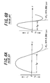
- Figs. 6, 7 and 8 are graphs showing the operation of the static induction thyristor used in the pulse generating circuit upon occurrence of discharge failure.
- Fig. 6 represent a variation of a current I ak flowing through the anode-cathode path
- Fig. 7 shows a variation of a gate current I g
- Fig. 8 denotes a variation of a gate voltage V g .
- A represents a case in which a pulse duration t w is long
- B shows a case in which a pulse duration t w is long.
- a pulse duration t w is set to a shorter value within a range from several hundreds ns to several ⁇ s, the reverse conducting static induction thyristor might be broken.
- a breakdown point situates in the static induction thyristor section and no abnormal phenomenon occurs in the diode section. From these phenomena, it is assumed that the breakdown of the reverse conducting static induction thyristor depends on an inclination of a raising portion of the current I ak .
- an inclination of a reverse current i r (di r /dt) is about 0.5 KA/ ⁇ s, and in the shorter pulse duration illustrated in Fig.
- an inclination of the reverse current is about 3 KA/ ⁇ s. Furthermore, as depicted in Fig. 8B, when the breakdown of the reverse conducting static induction thyristor due to discharge failure occurs, a remarkable variation appears in the gate voltage V g immediately after a reverse voltage peak.
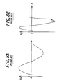
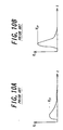
- Figs. 9 and 10 show a forward current I F flowing through the anode-cathode path of the diode 32 shown in Fig. 4 and a forward voltage drop V F appearing across the anode-cathode path of the diode when the diode is operated by a pulse.
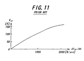
- A denotes a case of a smaller inclination and B represents a case of s larger inclination. From these graphs it can be understood that there is an intimate correlation between the inclination of the raising portion of the current IF and a transient on-voltage (forward recovery voltage) V FP as shown in Fig. 11.
- the forward recovery voltage V FP is lower such as about 70 V, but when the inclination of the current (dI F /dt) is high such as 1000A/ ⁇ s and 2000A/ ⁇ s, the forward recovery voltage V FP is becomes higher such as about 100 V and 170 V, respectively.
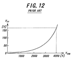
- Fig. 12 is a graph showing a relationship between the forward recovery voltage V FP and the breakdown voltage of the diode for the inclination dI F /dt of 2000 A/ ⁇ s.
- the forward recovery voltage V FP becomes higher.
- the forward recovery voltage V FP is about 170 V.
- the breakdown voltage of the diode section should be not lower than the breakdown voltage of the thyristor section, and therefore the diode section should have the breakdown voltage of several thousands volts.
- the diode section having such a high breakdown voltage also has a high forward recovery voltage V FP . In other words, the higher the breakdown voltage of the diode section is, the forward pulse current hardly flows through the diode section.
- the present invention has for its object to provide a novel and useful semiconductor device, in which the above mentioned problem of the known reverse conducting static induction thyristor, and even if a high reverse voltage is applied to a switching element abruptly, a protection diode can be brought into conductive and the switching element can be effectively protected from the breakdown.
- a semiconductor device having reverse conducting faculty comprises:
- said series arrangement of a plurality of diodes is formed in said first major surface of the semiconductor substrate in which said first main electrode region is also formed.
- Such a structure is particularly suitable for a high frequency pulse circuit in which inductance of wiring has to be reduced as far as possible.
- said series arrangement of a plurality of diodes may be formed on a separate semiconductor substrate from said semiconductor substrate semiconductor substrate which constitutes said switching element, or said series arrangement of a plurality of diodes may be formed as a diode stack including first and second electrodes connected to said first and second main electrodes of the switching element, respectively.
- said switching device and series arrangement of a plurality of diodes are installed in a common package in view of a reduction of wiring inductance.
- said switching device and series arrangement of a plurality of diodes may be in separate packages.
- said switching element is formed as a static induction thyristor whose cathode region and cathode electrode are formed by said first main electrode region and first main electrode, respectively, whose anode region and anode electrode are formed by said second main electrode region and second main electrode, respectively, and whose gate region and gate electrode are formed by said control region and control electrode, respectively.
- said switching element is formed as a reverse conducting static induction thyristor
- said series arrangement of a plurality of diodes are preferably formed as field limiting rings surrounding said static induction thyristor.
- a plurality of diodes of said series arrangement may be preferably formed such that breakdown voltages of the diodes are gradually increased toward outside.
- Fig. 13 is a schematic diagram showing a principal structure of the semiconductor device according to the invention.
- the switching element may be formed not only by a static induction thyristor, but also by another semiconductor switching element such as SCR and IGBT.
- the switching element is formed by a static induction thyristor.
- a series arrangement 63 of a plurality of diodes 62 is connected such that an anode of the series arrangement of diodes 63 is connected to the cathode K of the static induction thyristor 61 and a cathode of the series arrangement of diodes is connected to the anode A of the static induction thyristor, each of said plurality of diodes 62 having a breakdown voltage which is lower than a breakdown voltage of the static induction thyristor 61.
- the series arrangement 63 of diodes 62 is connected in parallel with the static induction thyristor in a reverse polarity.
- the breakdown voltages of these diodes 62 are set such that a sum of breakdown voltages of respective diodes becomes not less than the breakdown voltage of the static induction thyristor 61.
- the forward recovery voltage V FP of each diodes becomes about 10 V.
- Fig. 14 is a schematic diagram illustrating another principal structure of the semiconductor device according to the invention.
- the static induction thyristor is constructed as the reverse conducting static induction thyristor having a static induction thyristor section 61 and a diode section 64 connected in parallel with the static induction thyristor section 61 in a reverse polarity.
- a series arrangement 62 of a plurality of diodes 62 is connected in parallel with the reverse conducting static induction thyristor.
- the semiconductor device according to the invention having the above explained principal structures may be embodied in various ways.
- the series arrangement 63 of a plurality of diodes 62 may be formed on a same semiconductor substrate of the static induction thyristor 61 as a single unit.
- the semiconductor device when the semiconductor device is used in a high frequency circuit, it is necessary to make a stray inductance of wiring conductors as small as possible, and therefore it is preferable to construct the static induction thyristor 61 and series arrangement 63 of a plurality of diodes 62 in a single common semiconductor substrate.
- the series arrangement 63 of a plurality of diodes 62 may be constructed separately from a semiconductor substrate on which the static induction thyristor 61 is formed.
- the series arrangement 63 of diodes is preferably arranged within a package in which the static induction thyristor 61 is arranged, but it may be provided outside the package.
- This type of structure may be advantageously applied to the known semiconductor devices such as the static induction thyristor 61 shown in Fig. 13 and the reverse conducting static induction thyristor having the static induction thyristor 61 and the single diode 64 illustrated in Fig. 14.
- Figs. 15 and 16 are cross sectional views illustrating a first embodiment of the semiconductor device according to the invention having the principal structure shown in Fig. 14, in which the series arrangement 63 of a plurality of diodes 62 is connected in parallel with the switching element, i.e. static induction thyristor 61 as well as the single diode 64.
- a p + gate region (control region) 102 is formed substantially at a center area of one major surface of an n - silicon substrate 101, a plurality of first ring-shaped recesses 103 are formed to surround the gate region 102, and gate regions 104 are formed along the recesses 103.
- buried gate regions 105 are formed in channel regions formed by parts of the silicon substrate 101 surrounded by successive gate regions 102 and 104.
- conductive layers 106 On the gate regions 102 and 104 are formed conductive layers 106 and a gate electrode 107 is provided on the conductive layer at the central gate region 102.
- n + cathode regions (one major electrode region) 108 In surface portions of the channel regions, there are formed n + cathode regions (one major electrode region) 108 and the cathode regions are connected to a cathode electrode 110 via conductive layers 109.
- p + anode regions (the other major electrode region) 111 In the other major surface of the silicon substrate 101, there are formed p + anode regions (the other major electrode region) 111, which are connected to an anode electrode 113 via a conductive layer 112. In this manner, the thyristor section 114 is constructed.
- a p + anode region 131 of a main diode 134 outside the separation band 123, there is formed a p + anode region 131 of a main diode 134, said anode region having a wider width than the remaining p + regions 104 in the thyristor section 114.
- the anode region 131 is connected to the cathode electrode 110 via a conductive layer 132 of the thyristor section 114.
- a cathode region of the main diode section 134 is formed by a bulk of the n - silicon substrate 101 situating under the anode region 131.
- n + emitter region 133 which is connected to the anode electrode 113 of the thyristor section 144.
- the main diode section 134 serving to protect the thyristor section from the breakdown is formed such that the main diode section 134 is connected in parallel with the thyristor section 114 in a reverse polarity.
- the structure of the thyristor section 114, separation band 123 and main diode section 134 is identical with that of the known reverse conducting static induction thyristor.
- a plurality of ring-shaped third recesses 141 are formed to surround the main diode section 134, and in bottoms of these third recesses there are formed p + anode regions 142.
- each of the anode regions 142 is formed at a position deflected toward one side of the third recess 141.
- n + cathode contact regions 143 Between successive third recesses 141 there are formed n + cathode contact regions 143, and the successive cathode regions 143 are connected to adjacent p + anode regions 142 successively to constitute a series arrangement of a plurality of diodes by means of conductive layers 144. In this manner, a series arrangement section 145 is formed.
- exposed portions of the first major surface of the silicon substrate 101 are covered with insulating layers 146 such as silicon oxide layers as shown in Fig. 16.
- an anode region of the innermost diode in the series arrangement section 145 is formed by the anode region 131 of the main diode section 34, and a cathode of the outermost diode is connected to the anode electrode 113 of the static induction thyristor by means of the outermost cathode contact region 143 and conductive layers 147 and 112.
- the series arrangement section 145 in which the anode of the innermost diode is connected to the cathode electrode 110 of the thyristor and the cathode of the outermost diode is connected to the anode electrode 113.
- the main diode section 134 is connected in parallel with the series arrangement section 145 of a plurality of diodes.
- each of the plural diodes of the series arrangement section 145 has a breakdown voltage which is sufficiently lower than a breakdown voltage of the main diode section 134, and therefore its forward recovery voltage is sufficiently lower than that of the main diode section and energy loss due to the forward conduction becomes also very small.
- a reverse voltage is applied to the thyristor section 114, at first a plurality of diodes in the series arrangement section 145 are made conductive, and then the main diode section 134 is made conductive. In this manner, the thyristor section 134 can be effectively prevented from the breakdown.
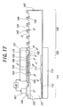
- Figs. 17 and 18 are cross sectional views illustrating a second embodiment of the semiconductor device according to the invention.
- the switching element is formed by the static induction thyristor without the main diode, and portions similar to those of the first embodiment are denoted by the same reference numerals used in Figs. 15 and 16.
- the ring-shaped recesses 141 formed in the series arrangement section 145 of a plurality of diodes are formed such that successive recesses viewed from the internal one have increasing widths so that the successive diodes have increasing breakdown voltage. Then, the p + anode regions 142 of these diodes serve optimally as a field limiting ring.
- the anode regions of a plurality of diodes of the series arrangement section 145 serve as the field limiting ring to some extent, but they do not optimally operate as the field limiting ring, because the third recesses 141 have identical width.
- the third recesses 141 formed in the series arrangement section 145 of a plurality of diodes have widths which are successively increased toward outside such that the p + anode regions 142 of the diodes work optimally as the field limiting ring.
- Such a structure may be easily realized by a known field limiting ring designing method.
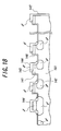
- Fig. 19 is a cross sectional view showing a third embodiment of the semiconductor device according to the invention.
- the switching element is formed by the static induction thyristor without a main diode. That is to say, in the first embodiment, the series arrangement section 145 of a plurality of diodes is provided in addition to the main diode section 134, but in the present embodiment the main diode section is not provided.
- a p + anode region of the innermost diode within the series arrangement 145 of a plurality of diodes is constituted by a p + region 122 within the separation band 123.
- the remaining structure of the present embodiment is identical with the above mentioned second embodiment.
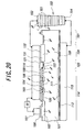
- Fig. 20 is a cross sectional view of a fourth embodiment of the semiconductor device according to the invention.
- the switching element is formed by the reverse conducting thyristor.
- the series arrangement of diodes is formed on the silicon substrate on which the thyristor is also formed.
- only the thyristor section 114, separation band 123 and main diode section 134 are formed on the silicon substrate 101, and a series arrangement 152 of a plurality of diodes 151 is provided separately from the silicon substrate 101.
- a reference numeral 161 denotes a field limiting ring section.
- the series arrangement of diodes may be formed on a semiconductor wafer like as the previous embodiment, but in the present embodiment, the series arrangement 152 of a plurality of diodes 151 is constructed by a diode stack. Furthermore, in the present embodiment, respective diodes 151 is constructed to have P + -i-n + structure and the series arrangement 152 is beveled such that a surface area of the diodes 151 is gradually decreased from the anode side to the cathode side.
- An anode electrode 153 of the series arrangement 152 of a plurality of diodes 151 is connected to the cathode electrode 110 of the thyristor section 114 and a cathode electrode 154 is connected to the anode electrode 113 of the thyristor section 114.
- the series arrangement 152 of a plurality of diodes 151 is preferably installed within a common package together with the silicon substrate 101 of the reverse conducting thyristor, but it may be installed in a separate package.
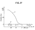
- Fig. 21 is a graph representing a breakdown rate of the semiconductor device according to the invention in comparison with the known reverse conducting static induction thyristor.
- the breakdown occurs in almost all samples when a width of a pulse voltage applied to the thyristor is not longer than 0.1 ⁇ s, i.e. when an inclination of a reverse current is not smaller than about 100 KA/ ⁇ s as shown by a curve A, and the breakdown occurs in a substantially half number of the samples at about 12 KA/ ⁇ s.
- the switching element formed on the semiconductor substrate is constituted by the static induction thyristor, but according to the invention, the switching element may be formed by any other switching element such as the gate turn-off (GTO) SCR and insulated gate bipolar transistor (IGBT).
- GTO gate turn-off
- IGBT insulated gate bipolar transistor
- the series arrangement of a plurality of diodes is connected in parallel with the switching element in a reverse polarity and each of these diodes has a breakdown voltage lower than a breakdown voltage of the switching element, when a current flowing through the switching element is abruptly decreased and a large reverse voltage is applied to the switching element, the series arrangement of diodes is positively conducted and the switching element can be-effectively prevented from breakdown.
- the series arrangement of diodes can be formed as a substantially same size as a conventional semiconductor device having the field limiting rings. Therefore, an increase in manufacturing cost can be restricted and an increase in cost of the semiconductor device according to the invention can be limited.
Landscapes
- Thyristors (AREA)
Abstract
Description
Claims (21)
- A semiconductor device having reverse conducting faculty comprising:a switching element including a semiconductor substrate of a first conductivity type having first and second major surfaces, a first main electrode region of the first conductivity type formed in the first major surface of the semiconductor substrate, a first main electrode connected to said first main electrode region, a second main electrode region of a second conductivity type formed in the second major surface of the semiconductor substrate, a second main electrode connected to said second main electrode region, a control electrode region of the second conductivity type formed in the first major surface of the semiconductor substrate for controlling a current passing between the first and second main electrode regions, and a control electrode connected to said control region; anda series arrangement of a plurality of diodes connected between said first main electrode and said second main electrode in an opposite polarity to a current flowing between said first main electrode region and said second main electrode region, each of said plurality of diodes having a breakdown voltage lower than a breakdown voltage of said switching element.
- The semiconductor device according to claim 1, wherein said series arrangement of a plurality of diodes is formed in said first major surface of the semiconductor substrate in which said first main electrode region is also formed.
- The semiconductor device according to claim 1, wherein said series arrangement of a plurality of diodes is formed on a separate semiconductor substrate from said semiconductor substrate semiconductor substrate which constitutes said switching element.
- The semiconductor device according to claim 1, wherein said series arrangement of a plurality of diodes is formed as a diode stack including first and second electrodes connected to said first and second main electrodes of the switching element, respectively.
- The semiconductor device according to claim 4, wherein said diode stack is beveled such that surface areas of successive diodes in the diode stack are gradually decreased viewed in a direction in which a current flows through the diode stack.
- The semiconductor device according to claim 4, wherein each of a plurality of diodes in the diode stack has p+-i-n+ structure.
- The semiconductor device according to any one of claims 3-6, wherein said switching device and series arrangement of a plurality of diodes are installed in a common package.
- The semiconductor device according to any one of claims 3-6, wherein said switching element and said series arrangement of a plurality of diodes are installed in separate packages.
- The semiconductor device according to claim 1, wherein said switching element is formed as a static induction thyristor whose cathode region and cathode electrode are formed by said first main electrode region and first main electrode, respectively, whose anode region and anode electrode are formed by said second main electrode region and second main electrode, respectively, and whose gate region and gate electrode are formed by said control region and control electrode, respectively.
- The semiconductor device according to claim 9, wherein said semiconductor substrate is formed by an n- semiconductor substrate, and said series arrangement of a plurality of diodes comprises a plurality of recesses formed in the first major surface of the n- semiconductor substrate, a plurality of p+ anode regions formed at bottom surfaces of said plurality of recesses, a plurality of n- cathode regions formed by portions of said first major surface of said n+ semiconductor substrate situating between successive recesses, a plurality of conductive layers formed on the first major surface of the n- semiconductor substrate via insulating layers such that said p+ anode regions and n+ cathode regions are successively connected by said conductive layers, and a cathode conductive layer for connecting an n+ cathode region of the outermost diode to said anode electrode of the static induction thyristor.
- The semiconductor device according to claim 10, wherein said series arrangement of a plurality of diodes further comprises a plurality of n+ cathode contact regions formed between said n- cathode regions and said conductive layers.
- The semiconductor device according to claim 10, wherein said recesses, anode regions and cathode regions of the series arrangement of a plurality of diodes are formed as ring-shape surrounding said static induction thyristor.
- The semiconductor device according to claim 12, wherein said recesses and anode regions of the series arrangement of a plurality of diodes are formed to serve as field limiting rings.
- The semiconductor device according to claim 12, wherein said recesses of the series arrangement of a plurality of diodes are formed such that widths of successive recesses are increased toward outside.
- The semiconductor device according to claim 1, wherein said switching element is formed as a reverse conducting static induction thyristor includinga thyristor section whose cathode region and cathode electrode are formed by said first main electrode region and first main electrode, respectively, whose anode region and anode electrode are formed by said second main electrode region and second main electrode, respectively, and whose gate region and gate electrode are formed by said control region and control electrode, respectively; anda main diode section having an anode region connected to said cathode electrode of the thyristor section and a cathode region connected to said anode electrode of the thyristor section.
- The semiconductor device according to claim 15, wherein said semiconductor substrate is formed by an n- semiconductor substrate;said main diode comprises a p+ anode region formed in said first major surface of the n- semiconductor substrate, said p+ anode region having a width longer than that of the gate regions of the thyristor section; andsaid series arrangement of a plurality of diodes comprises a plurality of recesses formed in the first major surface of the n- semiconductor substrate, a plurality of p+ anode regions formed at bottom surfaces of said plurality of recesses, a plurality of n- cathode regions formed by portions of said first major surface of said n- semiconductor substrate situating between successive recesses, a plurality of conductive layers formed on the first major surface of the n- semiconductor substrate via insulating layers such that said p+ anode regions and n+ cathode regions are successively connected by said conductive layers, and a cathode conductive layer for connecting an n+ cathode region of the outermost diode to said anode electrode of the static induction thyristor.
- The semiconductor device according to claim 16, wherein an anode region of the innermost diode of said series arrangement is formed by said p+ anode region of said main diode.
- The semiconductor device according to claim 16, wherein said series arrangement of a plurality of diodes further comprises a plurality of n+ cathode contact regions formed between said n- cathode regions and said conductive layers.
- The semiconductor device according to claim 16, wherein said recesses, anode regions and cathode regions of the series arrangement of a plurality of diodes are formed as ring-shape surrounding said thyristor section and main diode.
- The semiconductor device according to claim 19, wherein said recesses and anode regions of the series arrangement of a plurality of diodes are formed to serve as field limiting rings.
- The semiconductor device according to claim 20, wherein said recesses of the series arrangement of a plurality of diodes are formed such that widths of successive recesses are increased toward outside.
Applications Claiming Priority (2)
| Application Number | Priority Date | Filing Date | Title |
|---|---|---|---|
| JP2000030502 | 2000-02-08 | ||
| JP2000030502A JP4354069B2 (en) | 2000-02-08 | 2000-02-08 | Semiconductor device having reverse conduction function |
Publications (2)
| Publication Number | Publication Date |
|---|---|
| EP1124260A2 true EP1124260A2 (en) | 2001-08-16 |
| EP1124260A3 EP1124260A3 (en) | 2004-03-10 |
Family
ID=18555502
Family Applications (1)
| Application Number | Title | Priority Date | Filing Date |
|---|---|---|---|
| EP01301067A Withdrawn EP1124260A3 (en) | 2000-02-08 | 2001-02-07 | Semiconductor device with reverse conducting faculty |
Country Status (3)
| Country | Link |
|---|---|
| US (1) | US6403988B2 (en) |
| EP (1) | EP1124260A3 (en) |
| JP (1) | JP4354069B2 (en) |
Cited By (2)
| Publication number | Priority date | Publication date | Assignee | Title |
|---|---|---|---|---|
| WO2015192619A1 (en) * | 2014-06-17 | 2015-12-23 | 国家电网公司 | Synthesis loop-based testing apparatus and method for forward recovery characteristic of thyristor |
| CN106896258A (en) * | 2017-03-30 | 2017-06-27 | 西北核技术研究所 | A kind of IGCT transient state conduction voltage drop measuring circuit |
Families Citing this family (6)
| Publication number | Priority date | Publication date | Assignee | Title |
|---|---|---|---|---|
| US7321485B2 (en) | 1997-04-08 | 2008-01-22 | X2Y Attenuators, Llc | Arrangement for energy conditioning |
| JP4803965B2 (en) * | 2004-03-18 | 2011-10-26 | 日本碍子株式会社 | Junction gate type static induction thyristor and high voltage pulse generator using the junction gate type static induction thyristor |
| JP5052091B2 (en) * | 2006-10-20 | 2012-10-17 | 三菱電機株式会社 | Semiconductor device |
| JP5267036B2 (en) * | 2007-12-05 | 2013-08-21 | 株式会社デンソー | Manufacturing method of semiconductor device |
| US9406646B2 (en) * | 2011-10-27 | 2016-08-02 | Infineon Technologies Ag | Electronic device and method for fabricating an electronic device |
| JP7545365B2 (en) * | 2021-05-27 | 2024-09-04 | トヨタ自動車株式会社 | Cooling Structure |
Family Cites Families (10)
| Publication number | Priority date | Publication date | Assignee | Title |
|---|---|---|---|---|
| DE2238486A1 (en) * | 1972-08-04 | 1974-02-14 | Siemens Ag | THYRISTOR |
| SE414357B (en) * | 1978-08-17 | 1980-07-21 | Asea Ab | OVERVOLTAGE PROTECTION FOR PROTECTION OF SEMICONDUCTOR COMPONENTS OF LOW EFFECT TYPE |
| JPS56162867A (en) * | 1980-05-20 | 1981-12-15 | Toyo Electric Mfg Co Ltd | Composite thyristor |
| JPH0638707B2 (en) * | 1983-06-27 | 1994-05-18 | 株式会社日立製作所 | Control method of reverse conduction type gate turn-off type thyristor |
| JPH01102954A (en) * | 1987-10-16 | 1989-04-20 | Nissan Motor Co Ltd | Input protective circuit of semiconductor device |
| US4945266A (en) * | 1987-11-18 | 1990-07-31 | Mitsubishi Denki Kabushiki Kaisha | Composite semiconductor device |
| JPH0522099A (en) * | 1991-07-11 | 1993-01-29 | Nissan Motor Co Ltd | Semiconductor input protection circuit |
| US5682044A (en) * | 1995-01-31 | 1997-10-28 | Takashige Tamamushi | Reverse conducting thyristor with a planar-gate, buried-gate, or recessed-gate structure |
| US5679966A (en) * | 1995-10-05 | 1997-10-21 | North Carolina State University | Depleted base transistor with high forward voltage blocking capability |
| JPH09219510A (en) * | 1996-02-09 | 1997-08-19 | Toyo Electric Mfg Co Ltd | Reverse conduction semiconductor device |
-
2000
- 2000-02-08 JP JP2000030502A patent/JP4354069B2/en not_active Expired - Fee Related
-
2001
- 2001-02-02 US US09/776,577 patent/US6403988B2/en not_active Expired - Fee Related
- 2001-02-07 EP EP01301067A patent/EP1124260A3/en not_active Withdrawn
Cited By (3)
| Publication number | Priority date | Publication date | Assignee | Title |
|---|---|---|---|---|
| WO2015192619A1 (en) * | 2014-06-17 | 2015-12-23 | 国家电网公司 | Synthesis loop-based testing apparatus and method for forward recovery characteristic of thyristor |
| CN106896258A (en) * | 2017-03-30 | 2017-06-27 | 西北核技术研究所 | A kind of IGCT transient state conduction voltage drop measuring circuit |
| CN106896258B (en) * | 2017-03-30 | 2023-07-21 | 西北核技术研究所 | A Thyristor Transient Conduction Voltage Drop Measurement Circuit |
Also Published As
| Publication number | Publication date |
|---|---|
| US20010023963A1 (en) | 2001-09-27 |
| EP1124260A3 (en) | 2004-03-10 |
| JP2001223354A (en) | 2001-08-17 |
| US6403988B2 (en) | 2002-06-11 |
| JP4354069B2 (en) | 2009-10-28 |
Similar Documents
| Publication | Publication Date | Title |
|---|---|---|
| US6664590B2 (en) | Circuit configuration for load-relieved switching | |
| JP3804978B2 (en) | Converter circuit, circuit coupling arrangement having at least one switching device and circuit module | |
| US6933541B1 (en) | Emitter turn-off thyristors (ETO) | |
| US4755697A (en) | Bidirectional output semiconductor field effect transistor | |
| US6528826B2 (en) | Depletion type MOS semiconductor device and MOS power IC | |
| US4791470A (en) | Reverse conducting gate turn-off thyristor device | |
| US6403988B2 (en) | Semiconductor device with reverse conducting faculty | |
| US5463344A (en) | Fast turn on switch circuit with parallel MOS controlled thyristor and silicon controlled rectifier | |
| US5005061A (en) | Avalanche stress protected semiconductor device having variable input impedance | |
| US20130300487A1 (en) | Semiconductor switch | |
| JPH11274482A (en) | Semiconductor device | |
| JP2622524B2 (en) | Thyristor with turn-off mechanism and overvoltage protection means | |
| US4929856A (en) | Heavy-duty circuit breaker | |
| JPS62110435A (en) | Overvoltage protective integrated circuit device of subscriber line | |
| EP0077930B1 (en) | Gate turn-off thyristor | |
| US12495565B2 (en) | Bidirectional thyristor device with asymmetric characteristics | |
| US4357621A (en) | Reverse conducting thyristor with specific resistor structures between main cathode and amplifying, reverse conducting portions | |
| JP2004311901A (en) | Semiconductor device | |
| WO1999017374A1 (en) | Emitter turn-off thyristors (eto) | |
| US9553178B2 (en) | Semiconductor component with an emitter control electrode | |
| JP4278847B2 (en) | Reverse current protection circuit for power semiconductor switching element | |
| US5349213A (en) | Turn-off power semiconductor device | |
| JPS6248392B2 (en) | ||
| JP4129131B2 (en) | Semiconductor device | |
| JP5125899B2 (en) | Ignition device for internal combustion engine |
Legal Events
| Date | Code | Title | Description |
|---|---|---|---|
| PUAI | Public reference made under article 153(3) epc to a published international application that has entered the european phase |
Free format text: ORIGINAL CODE: 0009012 |
|
| AK | Designated contracting states |
Kind code of ref document: A2 Designated state(s): AT BE CH CY DE DK ES FI FR GB GR IE IT LI LU MC NL PT SE TR |
|
| AX | Request for extension of the european patent |
Free format text: AL;LT;LV;MK;RO;SI |
|
| PUAL | Search report despatched |
Free format text: ORIGINAL CODE: 0009013 |
|
| AK | Designated contracting states |
Kind code of ref document: A3 Designated state(s): AT BE CH CY DE DK ES FI FR GB GR IE IT LI LU MC NL PT SE TR |
|
| AX | Request for extension of the european patent |
Extension state: AL LT LV MK RO SI |
|
| RIC1 | Information provided on ipc code assigned before grant |
Ipc: 7H 01L 27/06 B Ipc: 7H 01L 27/08 A |
|
| AKX | Designation fees paid |
Designated state(s): CH DE FR GB LI |
|
| STAA | Information on the status of an ep patent application or granted ep patent |
Free format text: STATUS: THE APPLICATION IS DEEMED TO BE WITHDRAWN |
|
| 18D | Application deemed to be withdrawn |
Effective date: 20040911 |