EP1124148A1 - Apparatus for altering a light signal - Google Patents
Apparatus for altering a light signal Download PDFInfo
- Publication number
- EP1124148A1 EP1124148A1 EP01110557A EP01110557A EP1124148A1 EP 1124148 A1 EP1124148 A1 EP 1124148A1 EP 01110557 A EP01110557 A EP 01110557A EP 01110557 A EP01110557 A EP 01110557A EP 1124148 A1 EP1124148 A1 EP 1124148A1
- Authority
- EP
- European Patent Office
- Prior art keywords
- optical
- fiber
- light
- lens
- fibers
- Prior art date
- Legal status (The legal status is an assumption and is not a legal conclusion. Google has not performed a legal analysis and makes no representation as to the accuracy of the status listed.)
- Ceased
Links
Images


Classifications
-
- G—PHYSICS
- G02—OPTICS
- G02B—OPTICAL ELEMENTS, SYSTEMS OR APPARATUS
- G02B6/00—Light guides; Structural details of arrangements comprising light guides and other optical elements, e.g. couplings
- G02B6/24—Coupling light guides
- G02B6/26—Optical coupling means
- G02B6/32—Optical coupling means having lens focusing means positioned between opposed fibre ends
-
- G—PHYSICS
- G02—OPTICS
- G02B—OPTICAL ELEMENTS, SYSTEMS OR APPARATUS
- G02B6/00—Light guides; Structural details of arrangements comprising light guides and other optical elements, e.g. couplings
- G02B6/24—Coupling light guides
- G02B6/26—Optical coupling means
- G02B6/28—Optical coupling means having data bus means, i.e. plural waveguides interconnected and providing an inherently bidirectional system by mixing and splitting signals
- G02B6/2804—Optical coupling means having data bus means, i.e. plural waveguides interconnected and providing an inherently bidirectional system by mixing and splitting signals forming multipart couplers without wavelength selective elements, e.g. "T" couplers, star couplers
- G02B6/2817—Optical coupling means having data bus means, i.e. plural waveguides interconnected and providing an inherently bidirectional system by mixing and splitting signals forming multipart couplers without wavelength selective elements, e.g. "T" couplers, star couplers using reflective elements to split or combine optical signals
-
- G—PHYSICS
- G02—OPTICS
- G02B—OPTICAL ELEMENTS, SYSTEMS OR APPARATUS
- G02B6/00—Light guides; Structural details of arrangements comprising light guides and other optical elements, e.g. couplings
- G02B6/10—Light guides; Structural details of arrangements comprising light guides and other optical elements, e.g. couplings of the optical waveguide type
- G02B6/12—Light guides; Structural details of arrangements comprising light guides and other optical elements, e.g. couplings of the optical waveguide type of the integrated circuit kind
- G02B2006/12133—Functions
- G02B2006/12164—Multiplexing; Demultiplexing
-
- G—PHYSICS
- G02—OPTICS
- G02B—OPTICAL ELEMENTS, SYSTEMS OR APPARATUS
- G02B6/00—Light guides; Structural details of arrangements comprising light guides and other optical elements, e.g. couplings
- G02B6/24—Coupling light guides
- G02B6/36—Mechanical coupling means
- G02B6/3628—Mechanical coupling means for mounting fibres to supporting carriers
- G02B6/3632—Mechanical coupling means for mounting fibres to supporting carriers characterised by the cross-sectional shape of the mechanical coupling means
- G02B6/3636—Mechanical coupling means for mounting fibres to supporting carriers characterised by the cross-sectional shape of the mechanical coupling means the mechanical coupling means being grooves
-
- G—PHYSICS
- G02—OPTICS
- G02B—OPTICAL ELEMENTS, SYSTEMS OR APPARATUS
- G02B6/00—Light guides; Structural details of arrangements comprising light guides and other optical elements, e.g. couplings
- G02B6/24—Coupling light guides
- G02B6/36—Mechanical coupling means
- G02B6/3628—Mechanical coupling means for mounting fibres to supporting carriers
- G02B6/3648—Supporting carriers of a microbench type, i.e. with micromachined additional mechanical structures
- G02B6/3652—Supporting carriers of a microbench type, i.e. with micromachined additional mechanical structures the additional structures being prepositioning mounting areas, allowing only movement in one dimension, e.g. grooves, trenches or vias in the microbench surface, i.e. self aligning supporting carriers
-
- G—PHYSICS
- G02—OPTICS
- G02B—OPTICAL ELEMENTS, SYSTEMS OR APPARATUS
- G02B6/00—Light guides; Structural details of arrangements comprising light guides and other optical elements, e.g. couplings
- G02B6/24—Coupling light guides
- G02B6/36—Mechanical coupling means
- G02B6/3628—Mechanical coupling means for mounting fibres to supporting carriers
- G02B6/3684—Mechanical coupling means for mounting fibres to supporting carriers characterised by the manufacturing process of surface profiling of the supporting carrier
- G02B6/3692—Mechanical coupling means for mounting fibres to supporting carriers characterised by the manufacturing process of surface profiling of the supporting carrier with surface micromachining involving etching, e.g. wet or dry etching steps
-
- G—PHYSICS
- G02—OPTICS
- G02B—OPTICAL ELEMENTS, SYSTEMS OR APPARATUS
- G02B6/00—Light guides; Structural details of arrangements comprising light guides and other optical elements, e.g. couplings
- G02B6/24—Coupling light guides
- G02B6/42—Coupling light guides with opto-electronic elements
- G02B6/4201—Packages, e.g. shape, construction, internal or external details
- G02B6/4246—Bidirectionally operating package structures
Definitions
- the present invention relates to apparatus for altering a light signal.
- Fiber optics provides a low cost method for transmitting a light signal from one point to another.
- fiber optics allow transmission over paths having geometries that are more complex than the straight line segments provided by conventional optics.
- optical transmission systems have many advantages, these systems are particularly problematic when light from one fiber must coupled to a second fiber after being filtered or otherwise processed.
- the end of the first optical fiber is cut at an angle to prevent reflections from the glass-air interface from propagating back down the optical fiber.
- the cut fiber must be polished to prevent imperfections resulting from the cutting operation from generating back propagating reflections.
- an anti-reflective coating is applied to the cut and polished end to further reduce reflections. The cost of treating each cut end in this manner imposes economic constraints on the use of systems in which light must exit a fiber and pass through air.
- a second problem with such systems results from the high degree of alignment accuracy that is needed between the optical fibers.
- the ends must be aligned with a tolerance of the order of one micron.
- the fibers must be constrained from a rotational point of view. Even if one fiber is correctly fixed in space, the other fiber has two degrees of rotational freedom and three degrees of spatial freedom with respect to the fixed end of the first fiber.
- the high degree of alignment accuracy substantially increases the costs of systems of this type.
- European patent application 96301763.7 covers alignment apparatus which may be mass-produced at a much lower cost than prior art alignment mechanisms.
- the preferred embodiment of that application provides apparatus for aligning a plurality of optical fibers in predetermined positions with respect to one another.
- the apparatus includes a top plate and a bottom plate having a first set of alignment groves therein, there being one such grove corresponding to each optical fiber.
- the alignment groves are positioned such that the optical fibers will be in their correct positions with respect to one another when the optical fibers are forced against the bottom of the groves by the top plate.
- the optical flat also includes an anti-reflective material on the non-glued surface thereof.
- the bottom plate is preferably fabricated using photolithographic etching techniques similar to those used in mucro-machining and integrated circuit fabrication. This allows the bottom plates to be mass produced while maintaining the tight tolerances need for high light collection efficiencies.
- Various optical components can also be mounted on the bottom plates in groves with the aid of further groves in the bottom plates.
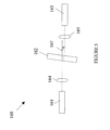
- Figure 1 illustrates the imaging of light from a first fiber 12 into a second fiber 14 by a lens 16.
- the ends of each fiber must be treated to avoid reflections generated at the glass-air interface from propagating back down the fiber.
- This treatment typically consists of cutting the end at an angle as shown at 18, polishing the end, and then coating the end with an anti-reflective coating. If a number of fibers must be positioned relative to one another, each end must be cut, polished, and coated.
- FIGS 2,3 and 4 illustrates an example of apparatus for aligning several optical fibers with respect to one another and for passivating the ends to reduce reflections, which is covered in European application 96301763.7.
- the required alignment tolerance is provided by a pedestal 102 which includes slots 104 that are positioned such that fibers that are forced against the bottom of each slot will be properly aligned with respect to one another. Exemplary fibers are shown at 105-110. The fibers are forced against slots 104 by top plate 112 which is preferably cemented to pedestal 102. The manner in which pedestal 102 is constructed will be discussed in more detail below.
- each fiber is cut at the desired angle by making a saw cut through the top plate 112. The cut extends into pedistal 102 as shown at 131 and 132. The saw cut severs each fiber at the correct angle. It should be noted that a single saw cut severs multiple fibers. In contrast to prior art systems, the ends of the optical fibers are not polished after the saw cut.
- a plate 146 is cemented to the fiber ends with the aid of a layer 145 of transparent cement.
- the index of refraction of the cement is chosen to match the index of the core of refraction of the fiber in the case of a single mode fiber. If the fiber is a GRIN lens, the index is chosen to match the index of the central region of the GRIN lens.
- Plate 146 is constructed from a material that has the same index of refraction as the cement layer. Hence, any scratches on the side of plate 146 that is in contact with the cement layer or on the cut fiber end are eliminated by the layer of cement.
- the surface 147 of plate 146 that is not in contact with the cement layer is preferably coated with an anti-reflective material to further reduce reflections.
- plate 146 is an inexpensive component that need only have one optically flat surface, i.e., surface 147.
- apparatus 100 can be constructed at a cost that is substantially less than the cost of systems in which the fiber ends are polished and coated with the anti-reflective material. It has been found experimentally, that the anti-reflection system described herein functions as well asthe conventional cut and polished end system. Thus,this system provides the benefits of the prior art systems at a substantially reduced cost.
- Pedestal 102 may be fabricated using conventional photo-lithography techniques. Such techniques provide the required alignment precision and are easily mass produced. Techniques for providing V-groves in Silicon or Ceramics are well known to the micro-machining arts. For example, in the case of a silicon substrate, a KOH etchant may be used. KOH provides a non-iostropic etch in which the etch rate of the (111) plane is so low that the etch process is practically stoped at the (111) planes. Hence, an etch mask oriented toward the (110) direction on a (100) silicon wafer will result in a V-groove formed by two (111) planes intercepting each other at a precise angle of 70.53°. The depth of the V-groove is solely determined by the width of the mask opening. Hence, two-dimensional lithography may be used to create a precise three-dimensional V-groove structure.
- optical component 162 is positioned such that the normal to its surface is at an angle with respect to the optical axis of optical fiber 161.
- this angular displacement results in the light leaving component 162 being displaced with respect to the optical axis of optical fiber 161 by an amount 167 that depends on the thickness and index of refraction of component 162.
- the alignment of optical fiber 163 must be tightly controlled to maintain high light collection efficiency.
- the system may be utilized to construct a universal optical platform for processing light traveling between four optical fibers or subsets thereof.
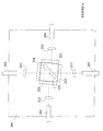
- a top view of such a platform is shown in Figure 6 at 200.
- Platform 200 processes light from optical fibers 202-205. Light may either enter or leave the platform via any of the fibers. The light leaving or entering a fiber is imaged or collimated by a corresponding lens. The lenses corresponding to optical fibers 202-205 are shown at 212-215, respectively. The actual processing of the light is performed by a coating applied to one or more of the 5 optical elements shown at 221-225.
- Platform 200 may be used to filter or polarize light traveling between two fibers that are opposite one another such as fibers 202 and 204. Platform 200 may also be used to construct a beam splitter or wavelength division multiplexer by utilizing the fibers that are arranged at right angles to these fibers.
- optical elements 221-225 All of the above described functions may be accomplished by utilizing different optical coatings on the optical elements 221-225. These optical elements are transparent and preferably planar. In the absence of any coatings on optical elements 221-225, the fibers are aligned such that light leaving fiber 202 is imaged into fiber 204. Similarly, light leaving fiber 205 is imaged into fiber 203. Finally, light leaving fiber 202 and reflected from optical element 225 is imaged into fiber 203. This alignment takes into account any beam walk-off produced by the passage of the light through the various optical elements. It should be noted that elements 221-224 are preferably positioned such that light reflected from their surfaces is not imaged back into fiber from which it originated.
- the platform on which the various components are mounted is preferably manufactured as described above. In all applications, all five of the optical components must be in place.
- one or more of the optical components are coated with thin film that provided the required optical processing. For example, if a beam splitter is to be constructed, the surface of optical element 225 is coated with a partially reflecting coating. If a filtering or polarizing operation is to be performed between fibers 202 and 204, the surface of either element 221 or 223 is coated. Since the coatings are much thinner than the optical elements, any walk-off resulting from a difference in thickness of the coated element can be neglected. Thus a single mass produced optical assembly may be used for a large number of applications without the need to align the apparatus for each new application.
- platform 200 utilized a lens that was separate from the adjacent optical element to image the light from the optical element into the corresponding optical fiber.
- the lens could be combined with the optical element if non-planar optical elements are acceptable.
- optical amplifiers may be constructed on such a platform.
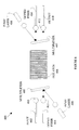
- the manner in which a typical optical amplifier operates may be more easily understood with reference to Figure 7 which is schematic drawing of a prior art Er-doped fiber example of an optical amplifier 300.
- Optical amplifier 300 amplifies a light signal input on a fiber 302.
- the input side of the fiber 302 is isolated by an optical isolator 303.
- the light is amplified in Er-doped fiber loop 305 which is pumped by lasers 304 and 306.
- the pumping light is coupled into loop 305 by wave division multiplexers (WDMs) 309 and 310.
- WDMs wave division multiplexers
- the amplified light from loop 305 is then filtered to remove any light at the pump frequency.
- the output end of fiber 302 is isolated from components on the output side of fiber 302 by isolator 307.
- the optical isolators prevent lasing in the amplifier by assuring that light only travels in one direction in Er-doped fiber loop 305.
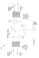
- FIG 8 is schematic drawing of an example of an Er-doped fiber optical amplifier for amplifying a signal received on optical fiber 404.
- the amplified light signal is coupled to optical fiber 410.
- the light signal received on optical fiber 402 is collimated by ball lens 403 and enters Er doped optical fiber 404 after passing through isolator 406 and WDM 407.
- Light from pump laser 408 is reflected from the surface of WDM 407 and also enters this end of doped fiber 404.
- Optical isolator 406 preforms functions analogous to isolators 303 and 307 shown in Figure 7.
- the light signal is amplified as it passes through doped fiber 404.
- the amplified signal is imaged by ball lens 412 into output fiber 410.
- a second pump laser 409 and WDM 405 are included in the preferred embodiment.
- the second pumping system allows the doped fiber to pumped from both ends.
- Optical isolator 406 prevents the light from pump laser 409 from escaping through output fiber 410.
- optical amplifier 400 eliminates one optical isolator. It should be noted that the cost of the optical isolators in optical amplifiers of the type shown in Figure 7 is a significant fraction of the cost of such amplifiers. Hence, this embodiment provides additional advantages over prior art optical amplifiers.
- FIG. 9 An alternative example of an optical amplifier is shown in Figure 9 at 500.
- This example utilizes two optical isolators 531 and 532 to assure that light travels in only one direction in Er-doped fiber 504; however, in contrast to optical amplifier 400, this embodiment requires only one pump laser.
- the input light is received on fiber 502, and the amplified light signal exits through fiber 510.
- the Er-doped fiber 504 is coupled to the amplifier via isolators 531 and 532.
- the Er-doped fiber is pumped by laser 525 which is coupled to the fiber 504 via WDM 522.
- Lenses 520-523 provide the required imaging functions. Lenses 520-521 couple the light from input fiber 520 into fiber 504, and the light exiting fiber 504 into output fiber 510. Lenses 523 images the pumping light into fiber 504.
- the invention also extends to apparatus for aligning a plurality of optical fibres in predetermined positions with respect to one another, the apparatus comprising a top plate; a bottom plate having a first set of alignment groves therein, there being one grove corresponding to each optical fibre, the alignment groves being positioned such that the optical fibres will be in the predetermined positions with respect to one another when the optical fibres are forced against the bottom of the groves by the top plate; and means for fastening the top and bottom plates such that the top plate forces the optical fibres against the groves in the bottom plate.
- At least one surface of the optical fibers is cut at an angle with respect to the axis of the optical fiber and wherein the cut end is bonded to an optical flat by a glue layer having the same index of refraction as the optical fiber.
- one surface of the optical flat is coated with an anti-reflective material.
- the groves in the bottom plate may be generated by photolithographically etching the bottom plate.
- the bottom plate comprises means for positioning an optical component with respect to the optical fibers.
- the optical component may be a lens.
- the optical fibers are arranged such that light leaving one of the optical fibers passes through a first lens, an optical element, a second lens and is imaged by the second lens into a second one of the optical fibers.
- the optical element comprises a optical isolator and a wave division multiplexer.
- the invention also extends to an optical amplifier comprising an input optical fiber for receiving a light signal at a predetermined wavelength to be amplified; a first pump light source; first wave division multiplexing means for focusing light from the first pump source into a first end of a doped optical fiber without blocking light at the wavelength of the light signal from exiting the first end of the doped optical fiber, the doped optical fiber being pumpable by the first pump light source; means for coupling light exiting a second end of the doped optical fiber into an output optical fiber; and optical isolation means for restricting the direction of travel of light in the doped optical fiber, wherein the optical isolation means is located between the first and second ends of the doped optical fiber.
- a second pump light source for focusing light from the second pump source into a second end of the doped optical fiber without blocking light at the wavelength of the light signal from entering the second end of the doped optical.
Abstract
Description
- The present invention relates to apparatus for altering a light signal.
- In many applications, optical transmission systems are utilized. Fiber optics provides a low cost method for transmitting a light signal from one point to another. In addition, fiber optics allow transmission over paths having geometries that are more complex than the straight line segments provided by conventional optics.
- While optical transmission systems have many advantages, these systems are particularly problematic when light from one fiber must coupled to a second fiber after being filtered or otherwise processed. Consider a system in which light leaves a first optical fiber, passes through an optical element of some sort, and is then re-imaged into a second optical fiber. In prior art systems, the end of the first optical fiber is cut at an angle to prevent reflections from the glass-air interface from propagating back down the optical fiber. In addition, the cut fiber must be polished to prevent imperfections resulting from the cutting operation from generating back propagating reflections. Finally, an anti-reflective coating is applied to the cut and polished end to further reduce reflections. The cost of treating each cut end in this manner imposes economic constraints on the use of systems in which light must exit a fiber and pass through air.
- A second problem with such systems results from the high degree of alignment accuracy that is needed between the optical fibers. For single mode fibers, the ends must be aligned with a tolerance of the order of one micron. In addition, the fibers must be constrained from a rotational point of view. Even if one fiber is correctly fixed in space, the other fiber has two degrees of rotational freedom and three degrees of spatial freedom with respect to the fixed end of the first fiber. The high degree of alignment accuracy substantially increases the costs of systems of this type.
- According to the present invention there is provided apparatus for altering a light signal as specified in claim 1.
- Other features are covered in European patent application 96301763.7, of which this is a divisional application, and in co-pending divisional patent application no. (RJ/N11019).
- It is also possible to provide an apparatus and method for reducing the reflectivity of cut fiber ends that does not require polishing of the ends.
- European patent application 96301763.7 covers alignment apparatus which may be mass-produced at a much lower cost than prior art alignment mechanisms. The preferred embodiment of that application provides apparatus for aligning a plurality of optical fibers in predetermined positions with respect to one another. The apparatus includes a top plate and a bottom plate having a first set of alignment groves therein, there being one such grove corresponding to each optical fiber. The alignment groves are positioned such that the optical fibers will be in their correct positions with respect to one another when the optical fibers are forced against the bottom of the groves by the top plate. To reduce reflections from cut fiber these optical fibers are cut at an angle with respect to the axis of the optical fiber, and the cut end is bonded to an optical flat by a glue layer having the same index of refraction as the optical fiber thereby preventing imperfections introduced by the cutting process from causing light to be reflected back into the fiber. Hence, the polishing steps used in prior art systems are avoided. In the preferred embodiment of the present invention, the optical flat also includes an anti-reflective material on the non-glued surface thereof. The bottom plate is preferably fabricated using photolithographic etching techniques similar to those used in mucro-machining and integrated circuit fabrication. This allows the bottom plates to be mass produced while maintaining the tight tolerances need for high light collection efficiencies. Various optical components can also be mounted on the bottom plates in groves with the aid of further groves in the bottom plates.
- An embodiment of the present invention is described below, by way of example only, with reference to the accompanying drawings, in which:
- Fig. 1 illustrates the preparation of fiber ends in applications in which light from a first fiber is imaged into a second fiber.
- Fig.2 is a top view of an embodiment of alignment apparatus covered in European application 96301763.7.
- Fig.3 is a cross-sectional view of the alignment apparatus shown in Figure 2 through line 120-121.
- Fig.4 is a cross-sectional view of the alignment apparatus shown in Figure 2 through line 122-123.
- Fig.5 is a cross-sectional view of an optical processing arrangement illustrating the alignment problems introduced by optical processing elements.
- Fig.6 is a top view of an embodiment of universal collimating platform.
- Fig.7 is a schematic drawing of a conventional optical amplifier.
- Fig.8 is a top view of an example of optical amplifier.
- Fig.9 is a top view of another example of optical amplifier.
-
- The preferred embodiment may be more easily understood with reference to Figure 1 which illustrates the imaging of light from a
first fiber 12 into asecond fiber 14 by alens 16. As noted above, the ends of each fiber must be treated to avoid reflections generated at the glass-air interface from propagating back down the fiber. This treatment typically consists of cutting the end at an angle as shown at 18, polishing the end, and then coating the end with an anti-reflective coating. If a number of fibers must be positioned relative to one another, each end must be cut, polished, and coated. - Now refer to Figures 2,3 and 4 which illustrates an example of apparatus for aligning several optical fibers with respect to one another and for passivating the ends to reduce reflections, which is covered in European application 96301763.7. The required alignment tolerance is provided by a
pedestal 102 which includesslots 104 that are positioned such that fibers that are forced against the bottom of each slot will be properly aligned with respect to one another. Exemplary fibers are shown at 105-110. The fibers are forced againstslots 104 bytop plate 112 which is preferably cemented topedestal 102. The manner in whichpedestal 102 is constructed will be discussed in more detail below. - In the example shown in Figures 2-4 the intervening optical components between each paid of fibers are indicated by blocks 133-135. Examples which specific optical elements will be discussed in more detail below.
Refer now to Figure 4 which illustrates the manner in which the ends of the optical fibers are treated to prevent light from reflecting back down the fibers at the glass-air interfaces. After the fibers have been secured against the bottom pedistal by the top plate, each fiber is cut at the desired angle by making a saw cut through thetop plate 112. The cut extends intopedistal 102 as shown at 131 and 132. The saw cut severs each fiber at the correct angle. It should be noted that a single saw cut severs multiple fibers. In contrast to prior art systems, the ends of the optical fibers are not polished after the saw cut. Instead, aplate 146 is cemented to the fiber ends with the aid of alayer 145 of transparent cement. The index of refraction of the cement is chosen to match the index of the core of refraction of the fiber in the case of a single mode fiber. If the fiber is a GRIN lens, the index is chosen to match the index of the central region of the GRIN lens.Plate 146 is constructed from a material that has the same index of refraction as the cement layer. Hence, any scratches on the side ofplate 146 that is in contact with the cement layer or on the cut fiber end are eliminated by the layer of cement. Thesurface 147 ofplate 146 that is not in contact with the cement layer is preferably coated with an anti-reflective material to further reduce reflections. - It should be noted that
plate 146 is an inexpensive component that need only have one optically flat surface, i.e.,surface 147. Hence, apparatus 100 can be constructed at a cost that is substantially less than the cost of systems in which the fiber ends are polished and coated with the anti-reflective material. It has been found experimentally, that the anti-reflection system described herein functions as well asthe conventional cut and polished end system. Thus,this system provides the benefits of the prior art systems at a substantially reduced cost. -
Pedestal 102 may be fabricated using conventional photo-lithography techniques. Such techniques provide the required alignment precision and are easily mass produced. Techniques for providing V-groves in Silicon or Ceramics are well known to the micro-machining arts. For example, in the case of a silicon substrate, a KOH etchant may be used. KOH provides a non-iostropic etch in which the etch rate of the (111) plane is so low that the etch process is practically stoped at the (111) planes. Hence, an etch mask oriented toward the (110) direction on a (100) silicon wafer will result in a V-groove formed by two (111) planes intercepting each other at a precise angle of 70.53°. The depth of the V-groove is solely determined by the width of the mask opening. Hence, two-dimensional lithography may be used to create a precise three-dimensional V-groove structure. - The ability to mass produce optical platforms having precise fixed alignment enables the system to be used for a number of optical components. In many applications light traveling down a first optical fiber must be filtered, polarized, or otherwise processed by some optical component before proceeding down a second optical fiber. The general arrangement for such processing is shown in Figure 5 at 160. Light traveling down
optical fiber 161 is collominated bylens 164 and than passes throughoptical component 162. Thelight leaving component 162 is then collected by asecond lens 165 which images that light into the outputoptical fiber 163. To eliminate reflections back downoptical fiber 161,optical component 162 is positioned such that the normal to its surface is at an angle with respect to the optical axis ofoptical fiber 161. Because of the difference in index of refraction ofcomponent 162 and air, this angular displacement results in thelight leaving component 162 being displaced with respect to the optical axis ofoptical fiber 161 by anamount 167 that depends on the thickness and index of refraction ofcomponent 162. As noted above, the alignment ofoptical fiber 163 must be tightly controlled to maintain high light collection efficiency. - In prior art optical processing systems, the cost of aligning the fibers for each different optical component is very high. The system provides means for mass producing very accurately aligned optical fibers and components; hence, an alignment platform is a significant improvement over the prior art.
- In particular, the system may be utilized to construct a universal optical platform for processing light traveling between four optical fibers or subsets thereof. A top view of such a platform is shown in Figure 6 at 200.
Platform 200 processes light from optical fibers 202-205. Light may either enter or leave the platform via any of the fibers. The light leaving or entering a fiber is imaged or collimated by a corresponding lens. The lenses corresponding to optical fibers 202-205 are shown at 212-215, respectively. The actual processing of the light is performed by a coating applied to one or more of the 5 optical elements shown at 221-225. -
Platform 200 may be used to filter or polarize light traveling between two fibers that are opposite one another such asfibers Platform 200 may also be used to construct a beam splitter or wavelength division multiplexer by utilizing the fibers that are arranged at right angles to these fibers. - All of the above described functions may be accomplished by utilizing different optical coatings on the optical elements 221-225. These optical elements are transparent and preferably planar. In the absence of any coatings on optical elements 221-225, the fibers are aligned such that
light leaving fiber 202 is imaged intofiber 204. Similarly,light leaving fiber 205 is imaged intofiber 203. Finally,light leaving fiber 202 and reflected fromoptical element 225 is imaged intofiber 203. This alignment takes into account any beam walk-off produced by the passage of the light through the various optical elements. It should be noted that elements 221-224 are preferably positioned such that light reflected from their surfaces is not imaged back into fiber from which it originated. - The platform on which the various components are mounted is preferably manufactured as described above. In all applications, all five of the optical components must be in place. For any particular application, one or more of the optical components are coated with thin film that provided the required optical processing. For example, if a beam splitter is to be constructed, the surface of
optical element 225 is coated with a partially reflecting coating. If a filtering or polarizing operation is to be performed betweenfibers element - The above described embodiment of
platform 200 utilized a lens that was separate from the adjacent optical element to image the light from the optical element into the corresponding optical fiber. However, it will be apparent to those skilled in the art that the lens could be combined with the optical element if non-planar optical elements are acceptable. - There are a number of other optical processing apparatuses that may advantageously be constructed using an optical alignment platform as described herein. For example, optical amplifiers may be constructed on such a platform. The manner in which a typical optical amplifier operates may be more easily understood with reference to Figure 7 which is schematic drawing of a prior art Er-doped fiber example of an
optical amplifier 300.Optical amplifier 300 amplifies a light signal input on afiber 302. The input side of thefiber 302 is isolated by anoptical isolator 303. The light is amplified in Er-dopedfiber loop 305 which is pumped bylasers loop 305 by wave division multiplexers (WDMs) 309 and 310. The amplified light fromloop 305 is then filtered to remove any light at the pump frequency. The output end offiber 302 is isolated from components on the output side offiber 302 byisolator 307. The optical isolators prevent lasing in the amplifier by assuring that light only travels in one direction in Er-dopedfiber loop 305. - Refer now to Figure 8 which is schematic drawing of an example of an Er-doped fiber optical amplifier for amplifying a signal received on
optical fiber 404. The amplified light signal is coupled tooptical fiber 410. The light signal received onoptical fiber 402 is collimated byball lens 403 and enters Er dopedoptical fiber 404 after passing throughisolator 406 andWDM 407. Light frompump laser 408 is reflected from the surface ofWDM 407 and also enters this end of dopedfiber 404.Optical isolator 406 preforms functions analogous toisolators fiber 404. The amplified signal is imaged byball lens 412 intooutput fiber 410. - To improve the pumping of doped
fiber 404, asecond pump laser 409 andWDM 405 are included in the preferred embodiment. The second pumping system allows the doped fiber to pumped from both ends.Optical isolator 406 prevents the light frompump laser 409 from escaping throughoutput fiber 410. - It should be noted that a single
optical isolator 406 performs the isolation functions of the two isolators described above with reference to the optical amplifier shown in Figure 7. Hence, in addition to providing an optical amplifier that can be assembled on an inexpensive mass-produced platform,optical amplifier 400 eliminates one optical isolator. It should be noted that the cost of the optical isolators in optical amplifiers of the type shown in Figure 7 is a significant fraction of the cost of such amplifiers. Hence, this embodiment provides additional advantages over prior art optical amplifiers. - An alternative example of an optical amplifier is shown in Figure 9 at 500. This example utilizes two
optical isolators fiber 504; however, in contrast tooptical amplifier 400, this embodiment requires only one pump laser. The input light is received onfiber 502, and the amplified light signal exits throughfiber 510. The Er-dopedfiber 504 is coupled to the amplifier viaisolators laser 525 which is coupled to thefiber 504 viaWDM 522. - Lenses 520-523 provide the required imaging functions. Lenses 520-521 couple the light from
input fiber 520 intofiber 504, and thelight exiting fiber 504 intooutput fiber 510.Lenses 523 images the pumping light intofiber 504. - The invention also extends to apparatus for aligning a plurality of optical fibres in predetermined positions with respect to one another, the apparatus comprising a top plate; a bottom plate having a first set of alignment groves therein, there being one grove corresponding to each optical fibre, the alignment groves being positioned such that the optical fibres will be in the predetermined positions with respect to one another when the optical fibres are forced against the bottom of the groves by the top plate; and means for fastening the top and bottom plates such that the top plate forces the optical fibres against the groves in the bottom plate.
- Preferably, at least one surface of the optical fibers is cut at an angle with respect to the axis of the optical fiber and wherein the cut end is bonded to an optical flat by a glue layer having the same index of refraction as the optical fiber.
- Advantageously, one surface of the optical flat is coated with an anti-reflective material.
- The groves in the bottom plate may be generated by photolithographically etching the bottom plate.
- Preferably, the bottom plate comprises means for positioning an optical component with respect to the optical fibers.
- The optical component may be a lens.
- In the preferred embodiment the optical fibers are arranged such that light leaving one of the optical fibers passes through a first lens, an optical element, a second lens and is imaged by the second lens into a second one of the optical fibers.
- Preferably, the optical element comprises a optical isolator and a wave division multiplexer.
- The invention also extends to an optical amplifier comprising an input optical fiber for receiving a light signal at a predetermined wavelength to be amplified; a first pump light source; first wave division multiplexing means for focusing light from the first pump source into a first end of a doped optical fiber without blocking light at the wavelength of the light signal from exiting the first end of the doped optical fiber, the doped optical fiber being pumpable by the first pump light source; means for coupling light exiting a second end of the doped optical fiber into an output optical fiber; and optical isolation means for restricting the direction of travel of light in the doped optical fiber, wherein the optical isolation means is located between the first and second ends of the doped optical fiber.
- Advantageously, there is provided a second pump light source; and second wave division multiplexing means for focusing light from the second pump source into a second end of the doped optical fiber without blocking light at the wavelength of the light signal from entering the second end of the doped optical.
- The disclosures in United States patent application no. 08/404,688, from which this application claims priority, in European patent application no. 96301763.7, of which this is a divisional patent application, and in the abstract accompanying this application are incorporated herein by reference.
Claims (2)
- Apparatus for altering a light signal comprising first, second, third and fourth optical fibres (202-205), each said optical fibre adapted for conducting light to or from said apparatus; first, second, third and fourth optical elements (221-224) corresponding, respectively, to said first, second, third and fourth optical fibres (202-205); first, second, third and fourth lenses (2112-215) corresponding, respectively, to said first, second, third and fourth optical fibres (202-205); and a fifth optical element (225), wherein each said lens is positioned with respect to said optical fibre corresponding to said lens such that light leaving said optical fibre and striking said lens from a first direction is collimated by said lens and collimated light entering said lens from a second direction is focused into said corresponding optical fibre, wherein said first (202) and third (204) optical fibres are positioned such that light entering said first optical fibre (202) traverses said first (221), third (223), and fifth (225) optical elements and is focused into said third optical fibre (204); wherein said second (205) and fourth (203) optical fibres are positioned such that light entering said second optical fibre (205) traverses said second (222), fourth (224), and fifth (225) optical elements and is focused into said fourth optical fibre (203); wherein said fifth optical element (225) is positioned such that a portion of the light leaving said first optical fibre (202) is reflected from the surface of said fifth optical element (225) into said fourth fibre (203) if said surface of said fifth optical element (225) is reflective, said portion depending on the degree of reflectivity of said surface of said fifth optical element (225), and wherein at least one surface of one of said optical elements includes a coating that alters the direction or composition of light striking said coating.
- Apparatus as in Claim 1, wherein said alteration caused by said coating depends on the wavelength of said light striking said coating.
Applications Claiming Priority (3)
| Application Number | Priority Date | Filing Date | Title |
|---|---|---|---|
| US08/404,688 US5528724A (en) | 1995-03-15 | 1995-03-15 | Apparatus and method for aligning optical fibers with respect to one another |
| US404688 | 1995-03-15 | ||
| EP96301763A EP0732603B1 (en) | 1995-03-15 | 1996-03-14 | Optical fiber alignment |
Related Parent Applications (1)
| Application Number | Title | Priority Date | Filing Date |
|---|---|---|---|
| EP96301763A Division EP0732603B1 (en) | 1995-03-15 | 1996-03-14 | Optical fiber alignment |
Publications (1)
| Publication Number | Publication Date |
|---|---|
| EP1124148A1 true EP1124148A1 (en) | 2001-08-16 |
Family
ID=23600626
Family Applications (3)
| Application Number | Title | Priority Date | Filing Date |
|---|---|---|---|
| EP96301763A Expired - Lifetime EP0732603B1 (en) | 1995-03-15 | 1996-03-14 | Optical fiber alignment |
| EP01110557A Ceased EP1124148A1 (en) | 1995-03-15 | 1996-03-14 | Apparatus for altering a light signal |
| EP01110558A Expired - Lifetime EP1124149B1 (en) | 1995-03-15 | 1996-03-14 | Optical amplifier |
Family Applications Before (1)
| Application Number | Title | Priority Date | Filing Date |
|---|---|---|---|
| EP96301763A Expired - Lifetime EP0732603B1 (en) | 1995-03-15 | 1996-03-14 | Optical fiber alignment |
Family Applications After (1)
| Application Number | Title | Priority Date | Filing Date |
|---|---|---|---|
| EP01110558A Expired - Lifetime EP1124149B1 (en) | 1995-03-15 | 1996-03-14 | Optical amplifier |
Country Status (4)
| Country | Link |
|---|---|
| US (1) | US5528724A (en) |
| EP (3) | EP0732603B1 (en) |
| JP (1) | JP3902680B2 (en) |
| DE (2) | DE69629064T2 (en) |
Cited By (2)
| Publication number | Priority date | Publication date | Assignee | Title |
|---|---|---|---|---|
| WO2003079084A1 (en) * | 2002-03-14 | 2003-09-25 | Corning Incorporated | Optical fiber positioning device and methods of manufacture |
| US6928226B2 (en) | 2002-03-14 | 2005-08-09 | Corning Incorporated | Fiber and lens grippers, optical devices and methods of manufacture |
Families Citing this family (14)
| Publication number | Priority date | Publication date | Assignee | Title |
|---|---|---|---|---|
| US6049650A (en) * | 1998-04-17 | 2000-04-11 | Seagate Technology, Inc. | Structure for micro-machine optical tooling and method for making and using |
| US6473553B1 (en) | 1998-04-17 | 2002-10-29 | Seagate Technology Llc | Apparatus for holding and engaging micro-machined objects and method for making same |
| US6075642A (en) * | 1998-06-18 | 2000-06-13 | Hewlett-Packard Company | Multi-port optical isolator |
| US6747793B1 (en) * | 1999-11-15 | 2004-06-08 | Axsun Technologies, Inc. | System with integrated semiconductor optical amplifier array and switching matrix |
| JP2001305376A (en) * | 2000-02-17 | 2001-10-31 | Nippon Sheet Glass Co Ltd | Method for designing collimator array device and collimator array device manufactured by the method |
| JP2002255580A (en) * | 2000-12-27 | 2002-09-11 | Nippon Sheet Glass Co Ltd | Method for cutting perform of rod lens and lens block to be used for the same |
| US6434314B1 (en) * | 2001-03-13 | 2002-08-13 | 3M Innovative Properties Company | Force equalizing filament clamp |
| US6772609B2 (en) * | 2001-12-13 | 2004-08-10 | Corning Incorporated | Multi-lens finishing process |
| JP2003337259A (en) * | 2002-05-21 | 2003-11-28 | Ricoh Opt Ind Co Ltd | Array type multi-fiber optical connector |
| JP4540951B2 (en) * | 2003-08-12 | 2010-09-08 | 株式会社フジクラ | Matrix light switch |
| JP2008003637A (en) * | 2004-03-31 | 2008-01-10 | Hitachi Chem Co Ltd | Optical element-binding structure and optical fiber structure |
| US8503840B2 (en) | 2010-08-23 | 2013-08-06 | Lockheed Martin Corporation | Optical-fiber array method and apparatus |
| WO2011130131A1 (en) | 2010-04-12 | 2011-10-20 | Lockheed Martin Corporation | Beam diagnostics and feedback system and method for spectrally beam-combined lasers |
| US11446776B2 (en) * | 2020-08-27 | 2022-09-20 | Northrop Grumman Systems Corporation | Method for assembling a hollow core optical fiber array launcher |
Citations (5)
| Publication number | Priority date | Publication date | Assignee | Title |
|---|---|---|---|---|
| JPS54146644A (en) * | 1978-05-09 | 1979-11-16 | Mitsubishi Electric Corp | Light distributor |
| JPS62138837A (en) * | 1985-12-12 | 1987-06-22 | Hitachi Ltd | Optical path change-over switch |
| US4720162A (en) * | 1981-05-11 | 1988-01-19 | Kokusai Denshin Denwa Kabushiki Kaisha | Device for switching from one light source to another |
| JPH0346637A (en) * | 1989-07-14 | 1991-02-27 | Nec Corp | Optical amplifier and optical amplifying method |
| EP0640853A1 (en) * | 1993-08-31 | 1995-03-01 | Fujitsu Limited | Hybrid type integrated optical device having double-layered substrate |
Family Cites Families (12)
| Publication number | Priority date | Publication date | Assignee | Title |
|---|---|---|---|---|
| DE2658067C3 (en) * | 1976-12-22 | 1980-11-06 | The Deutsch Company Electronic Components Division, Banning, Calif. (V.St.A.) | Optical connector |
| US4265513A (en) * | 1978-08-17 | 1981-05-05 | Nippon Electric Co., Ltd. | Light switch |
| DE3615727A1 (en) * | 1986-05-09 | 1987-11-12 | Zeiss Carl Fa | COUPLING POINT FOR MONOMODE FIBER |
| US4778243A (en) * | 1986-12-08 | 1988-10-18 | Siemens Aktiengesellschaft | Connector element for a light waveguide |
| JPS63289509A (en) * | 1987-05-22 | 1988-11-28 | Furukawa Electric Co Ltd:The | Multi-cored optical parts and its production |
| AU635172B2 (en) * | 1991-05-13 | 1993-03-11 | Nippon Telegraph & Telephone Corporation | Multifiber optical connector plug with low reflection and low insertion loss |
| US5191467A (en) * | 1991-07-24 | 1993-03-02 | Kaptron, Inc. | Fiber optic isolater and amplifier |
| JPH05307116A (en) * | 1992-05-01 | 1993-11-19 | Sumitomo Electric Ind Ltd | Optical fiber clamp |
| US5257332A (en) * | 1992-09-04 | 1993-10-26 | At&T Bell Laboratories | Optical fiber expanded beam coupler |
| JPH06252478A (en) * | 1993-02-26 | 1994-09-09 | Ando Electric Co Ltd | Optical fiber ring laser |
| US5359683A (en) * | 1993-06-10 | 1994-10-25 | Advanced Optronics, Inc. | 1×N electromechanical optical switch |
| GB2293024A (en) * | 1994-09-07 | 1996-03-13 | Northern Telecom Ltd | Optical isolator functioning at least twice in different pathways |
-
1995
- 1995-03-15 US US08/404,688 patent/US5528724A/en not_active Expired - Fee Related
-
1996
- 1996-02-21 JP JP03351396A patent/JP3902680B2/en not_active Expired - Fee Related
- 1996-03-14 DE DE69629064T patent/DE69629064T2/en not_active Expired - Fee Related
- 1996-03-14 EP EP96301763A patent/EP0732603B1/en not_active Expired - Lifetime
- 1996-03-14 DE DE69625838T patent/DE69625838T2/en not_active Expired - Fee Related
- 1996-03-14 EP EP01110557A patent/EP1124148A1/en not_active Ceased
- 1996-03-14 EP EP01110558A patent/EP1124149B1/en not_active Expired - Lifetime
Patent Citations (5)
| Publication number | Priority date | Publication date | Assignee | Title |
|---|---|---|---|---|
| JPS54146644A (en) * | 1978-05-09 | 1979-11-16 | Mitsubishi Electric Corp | Light distributor |
| US4720162A (en) * | 1981-05-11 | 1988-01-19 | Kokusai Denshin Denwa Kabushiki Kaisha | Device for switching from one light source to another |
| JPS62138837A (en) * | 1985-12-12 | 1987-06-22 | Hitachi Ltd | Optical path change-over switch |
| JPH0346637A (en) * | 1989-07-14 | 1991-02-27 | Nec Corp | Optical amplifier and optical amplifying method |
| EP0640853A1 (en) * | 1993-08-31 | 1995-03-01 | Fujitsu Limited | Hybrid type integrated optical device having double-layered substrate |
Non-Patent Citations (3)
| Title |
|---|
| PATENT ABSTRACTS OF JAPAN vol. 004, no. 005 (E - 165) 16 January 1980 (1980-01-16) * |
| PATENT ABSTRACTS OF JAPAN vol. 011, no. 366 (P - 641) 28 November 1987 (1987-11-28) * |
| PATENT ABSTRACTS OF JAPAN vol. 015, no. 196 (P - 1203) 21 May 1991 (1991-05-21) * |
Cited By (2)
| Publication number | Priority date | Publication date | Assignee | Title |
|---|---|---|---|---|
| WO2003079084A1 (en) * | 2002-03-14 | 2003-09-25 | Corning Incorporated | Optical fiber positioning device and methods of manufacture |
| US6928226B2 (en) | 2002-03-14 | 2005-08-09 | Corning Incorporated | Fiber and lens grippers, optical devices and methods of manufacture |
Also Published As
| Publication number | Publication date |
|---|---|
| EP1124149A2 (en) | 2001-08-16 |
| EP1124149A3 (en) | 2001-08-22 |
| DE69625838T2 (en) | 2003-09-25 |
| EP0732603B1 (en) | 2003-01-22 |
| JP3902680B2 (en) | 2007-04-11 |
| DE69629064D1 (en) | 2003-08-14 |
| US5528724A (en) | 1996-06-18 |
| JPH08262255A (en) | 1996-10-11 |
| EP0732603A3 (en) | 1997-08-27 |
| EP0732603A2 (en) | 1996-09-18 |
| EP1124149B1 (en) | 2003-07-09 |
| DE69625838D1 (en) | 2003-02-27 |
| DE69629064T2 (en) | 2004-04-22 |
Similar Documents
| Publication | Publication Date | Title |
|---|---|---|
| EP1124149B1 (en) | Optical amplifier | |
| US5267077A (en) | Spherical multicomponent optical isolator | |
| US6563976B1 (en) | Cost-effective wavelength division multiplexer and demultiplexer | |
| US6198864B1 (en) | Optical wavelength demultiplexer | |
| US5699463A (en) | Mechanical fiber optic switch | |
| FI82778C (en) | LJUSVAOGLEDARFOERGRENING. | |
| EP0722101B1 (en) | Optical fiber ferrule and optical coupler constructed using the optical fiber ferrule | |
| EP0642045A1 (en) | Hybrid optical IC with optical axes at different level | |
| CA2370746C (en) | Wavelength compensated optical wavelength division coupler and associated methods | |
| EP3182180B1 (en) | Multichannel fiber optic rotary joint(forj) having an achromatic metasurface | |
| JPS6145801B2 (en) | ||
| US20080118243A1 (en) | Compact optical multiplexer and demultiplexer | |
| JPH1172748A (en) | Optical isolator and wavelength multiplexer module having integrated optical isolator | |
| JP3130499B2 (en) | Three-port optical circulator and method of manufacturing the same | |
| JPH0854532A (en) | Integral device | |
| US7315673B2 (en) | Optical multiplexer/demultiplexer and method of manufacturing the same | |
| JP3151699B2 (en) | Fabrication method of optical circuit components | |
| JPH10268158A (en) | Optical branching filter and optical coupling part | |
| US20040001677A1 (en) | Telescopic collimator and method of manufacture | |
| JPH11218638A (en) | Optical constituent element | |
| JP4632227B2 (en) | Optical module | |
| JPH11190809A (en) | Multiplexer demultiplexer | |
| JPS6330605B2 (en) | ||
| JP2003329874A (en) | Optical module and method for manufacturing the same | |
| Mizuno et al. | A bidirectional optical module based on stacked planar optical circuit |
Legal Events
| Date | Code | Title | Description |
|---|---|---|---|
| PUAI | Public reference made under article 153(3) epc to a published international application that has entered the european phase |
Free format text: ORIGINAL CODE: 0009012 |
|
| 17P | Request for examination filed |
Effective date: 20010514 |
|
| AC | Divisional application: reference to earlier application |
Ref document number: 732603 Country of ref document: EP |
|
| AK | Designated contracting states |
Kind code of ref document: A1 Designated state(s): DE FR GB |
|
| RAP1 | Party data changed (applicant data changed or rights of an application transferred) |
Owner name: AGILENT TECHNOLOGIES, INC. (A DELAWARE CORPORATION |
|
| RIN1 | Information on inventor provided before grant (corrected) |
Inventor name: YANG, LONG Inventor name: CHANG, KOK-WAL |
|
| AKX | Designation fees paid |
Free format text: DE FR GB |
|
| 17Q | First examination report despatched |
Effective date: 20020902 |
|
| APBN | Date of receipt of notice of appeal recorded |
Free format text: ORIGINAL CODE: EPIDOSNNOA2E |
|
| APBR | Date of receipt of statement of grounds of appeal recorded |
Free format text: ORIGINAL CODE: EPIDOSNNOA3E |
|
| APAA | Appeal reference recorded |
Free format text: ORIGINAL CODE: EPIDOS REFN |
|
| APAF | Appeal reference modified |
Free format text: ORIGINAL CODE: EPIDOSCREFNE |
|
| APBT | Appeal procedure closed |
Free format text: ORIGINAL CODE: EPIDOSNNOA9E |
|
| RAP1 | Party data changed (applicant data changed or rights of an application transferred) |
Owner name: AVAGO TECHNOLOGIES FIBER IP (SINGAPORE) PTE. LTD. |
|
| STAA | Information on the status of an ep patent application or granted ep patent |
Free format text: STATUS: THE APPLICATION HAS BEEN REFUSED |
|
| 18R | Application refused |
Effective date: 20091019 |