EP1123753A2 - Mesoporous ceramic films having reduced dielectric constants - Google Patents
Mesoporous ceramic films having reduced dielectric constants Download PDFInfo
- Publication number
- EP1123753A2 EP1123753A2 EP00126445A EP00126445A EP1123753A2 EP 1123753 A2 EP1123753 A2 EP 1123753A2 EP 00126445 A EP00126445 A EP 00126445A EP 00126445 A EP00126445 A EP 00126445A EP 1123753 A2 EP1123753 A2 EP 1123753A2
- Authority
- EP
- European Patent Office
- Prior art keywords
- film
- ceramic
- surfactant
- solution
- less
- Prior art date
- Legal status (The legal status is an assumption and is not a legal conclusion. Google has not performed a legal analysis and makes no representation as to the accuracy of the status listed.)
- Granted
Links
Images


Classifications
-
- H—ELECTRICITY
- H10—SEMICONDUCTOR DEVICES; ELECTRIC SOLID-STATE DEVICES NOT OTHERWISE PROVIDED FOR
- H10P—GENERIC PROCESSES OR APPARATUS FOR THE MANUFACTURE OR TREATMENT OF DEVICES COVERED BY CLASS H10
- H10P14/00—Formation of materials, e.g. in the shape of layers or pillars
- H10P14/60—Formation of materials, e.g. in the shape of layers or pillars of insulating materials
- H10P14/69—Inorganic materials
- H10P14/692—Inorganic materials composed of oxides, glassy oxides or oxide-based glasses
- H10P14/6921—Inorganic materials composed of oxides, glassy oxides or oxide-based glasses containing silicon
- H10P14/6922—Inorganic materials composed of oxides, glassy oxides or oxide-based glasses containing silicon the material containing Si, O and at least one of H, N, C, F or other non-metal elements, e.g. SiOC, SiOC:H or SiONC
-
- C—CHEMISTRY; METALLURGY
- C08—ORGANIC MACROMOLECULAR COMPOUNDS; THEIR PREPARATION OR CHEMICAL WORKING-UP; COMPOSITIONS BASED THEREON
- C08G—MACROMOLECULAR COMPOUNDS OBTAINED OTHERWISE THAN BY REACTIONS ONLY INVOLVING UNSATURATED CARBON-TO-CARBON BONDS
- C08G77/00—Macromolecular compounds obtained by reactions forming a linkage containing silicon with or without sulfur, nitrogen, oxygen or carbon in the main chain of the macromolecule
- C08G77/60—Macromolecular compounds obtained by reactions forming a linkage containing silicon with or without sulfur, nitrogen, oxygen or carbon in the main chain of the macromolecule in which all the silicon atoms are connected by linkages other than oxygen atoms
- C08G77/62—Nitrogen atoms
-
- C—CHEMISTRY; METALLURGY
- C08—ORGANIC MACROMOLECULAR COMPOUNDS; THEIR PREPARATION OR CHEMICAL WORKING-UP; COMPOSITIONS BASED THEREON
- C08K—Use of inorganic or non-macromolecular organic substances as compounding ingredients
- C08K5/00—Use of organic ingredients
- C08K5/56—Organo-metallic compounds, i.e. organic compounds containing a metal-to-carbon bond
-
- C—CHEMISTRY; METALLURGY
- C08—ORGANIC MACROMOLECULAR COMPOUNDS; THEIR PREPARATION OR CHEMICAL WORKING-UP; COMPOSITIONS BASED THEREON
- C08L—COMPOSITIONS OF MACROMOLECULAR COMPOUNDS
- C08L53/00—Compositions of block copolymers containing at least one sequence of a polymer obtained by reactions only involving carbon-to-carbon unsaturated bonds; Compositions of derivatives of such polymers
-
- C—CHEMISTRY; METALLURGY
- C09—DYES; PAINTS; POLISHES; NATURAL RESINS; ADHESIVES; COMPOSITIONS NOT OTHERWISE PROVIDED FOR; APPLICATIONS OF MATERIALS NOT OTHERWISE PROVIDED FOR
- C09D—COATING COMPOSITIONS, e.g. PAINTS, VARNISHES OR LACQUERS; FILLING PASTES; CHEMICAL PAINT OR INK REMOVERS; INKS; CORRECTING FLUIDS; WOODSTAINS; PASTES OR SOLIDS FOR COLOURING OR PRINTING; USE OF MATERIALS THEREFOR
- C09D153/00—Coating compositions based on block copolymers containing at least one sequence of a polymer obtained by reactions only involving carbon-to-carbon unsaturated bonds; Coating compositions based on derivatives of such polymers
-
- C—CHEMISTRY; METALLURGY
- C09—DYES; PAINTS; POLISHES; NATURAL RESINS; ADHESIVES; COMPOSITIONS NOT OTHERWISE PROVIDED FOR; APPLICATIONS OF MATERIALS NOT OTHERWISE PROVIDED FOR
- C09D—COATING COMPOSITIONS, e.g. PAINTS, VARNISHES OR LACQUERS; FILLING PASTES; CHEMICAL PAINT OR INK REMOVERS; INKS; CORRECTING FLUIDS; WOODSTAINS; PASTES OR SOLIDS FOR COLOURING OR PRINTING; USE OF MATERIALS THEREFOR
- C09D183/00—Coating compositions based on macromolecular compounds obtained by reactions forming in the main chain of the macromolecule a linkage containing silicon, with or without sulfur, nitrogen, oxygen, or carbon only; Coating compositions based on derivatives of such polymers
- C09D183/16—Coating compositions based on macromolecular compounds obtained by reactions forming in the main chain of the macromolecule a linkage containing silicon, with or without sulfur, nitrogen, oxygen, or carbon only; Coating compositions based on derivatives of such polymers in which all the silicon atoms are connected by linkages other than oxygen atoms
-
- H—ELECTRICITY
- H10—SEMICONDUCTOR DEVICES; ELECTRIC SOLID-STATE DEVICES NOT OTHERWISE PROVIDED FOR
- H10P—GENERIC PROCESSES OR APPARATUS FOR THE MANUFACTURE OR TREATMENT OF DEVICES COVERED BY CLASS H10
- H10P14/00—Formation of materials, e.g. in the shape of layers or pillars
- H10P14/60—Formation of materials, e.g. in the shape of layers or pillars of insulating materials
- H10P14/65—Formation of materials, e.g. in the shape of layers or pillars of insulating materials characterised by treatments performed before or after the formation of the materials
- H10P14/6516—Formation of materials, e.g. in the shape of layers or pillars of insulating materials characterised by treatments performed before or after the formation of the materials of treatments performed after formation of the materials
- H10P14/6529—Formation of materials, e.g. in the shape of layers or pillars of insulating materials characterised by treatments performed before or after the formation of the materials of treatments performed after formation of the materials by exposure to a gas or vapour
-
- H—ELECTRICITY
- H10—SEMICONDUCTOR DEVICES; ELECTRIC SOLID-STATE DEVICES NOT OTHERWISE PROVIDED FOR
- H10P—GENERIC PROCESSES OR APPARATUS FOR THE MANUFACTURE OR TREATMENT OF DEVICES COVERED BY CLASS H10
- H10P14/00—Formation of materials, e.g. in the shape of layers or pillars
- H10P14/60—Formation of materials, e.g. in the shape of layers or pillars of insulating materials
- H10P14/66—Formation of materials, e.g. in the shape of layers or pillars of insulating materials characterised by the type of materials
- H10P14/668—Formation of materials, e.g. in the shape of layers or pillars of insulating materials characterised by the type of materials the materials being characterised by the deposition precursor materials
- H10P14/6681—Formation of materials, e.g. in the shape of layers or pillars of insulating materials characterised by the type of materials the materials being characterised by the deposition precursor materials the precursor containing a compound comprising Si
- H10P14/6687—Formation of materials, e.g. in the shape of layers or pillars of insulating materials characterised by the type of materials the materials being characterised by the deposition precursor materials the precursor containing a compound comprising Si the compound comprising silicon and nitrogen
- H10P14/6689—Formation of materials, e.g. in the shape of layers or pillars of insulating materials characterised by the type of materials the materials being characterised by the deposition precursor materials the precursor containing a compound comprising Si the compound comprising silicon and nitrogen the compound being a silazane
-
- H—ELECTRICITY
- H10—SEMICONDUCTOR DEVICES; ELECTRIC SOLID-STATE DEVICES NOT OTHERWISE PROVIDED FOR
- H10P—GENERIC PROCESSES OR APPARATUS FOR THE MANUFACTURE OR TREATMENT OF DEVICES COVERED BY CLASS H10
- H10P14/00—Formation of materials, e.g. in the shape of layers or pillars
- H10P14/60—Formation of materials, e.g. in the shape of layers or pillars of insulating materials
- H10P14/69—Inorganic materials
- H10P14/692—Inorganic materials composed of oxides, glassy oxides or oxide-based glasses
- H10P14/6921—Inorganic materials composed of oxides, glassy oxides or oxide-based glasses containing silicon
- H10P14/6928—Inorganic materials composed of oxides, glassy oxides or oxide-based glasses containing silicon the material containing silicon and at least one metal element, e.g. metal silicate based insulators or metal silicon oxynitrides
- H10P14/6929—Inorganic materials composed of oxides, glassy oxides or oxide-based glasses containing silicon the material containing silicon and at least one metal element, e.g. metal silicate based insulators or metal silicon oxynitrides the material containing aluminium, e.g. AlSiOx
-
- H—ELECTRICITY
- H10—SEMICONDUCTOR DEVICES; ELECTRIC SOLID-STATE DEVICES NOT OTHERWISE PROVIDED FOR
- H10P—GENERIC PROCESSES OR APPARATUS FOR THE MANUFACTURE OR TREATMENT OF DEVICES COVERED BY CLASS H10
- H10P14/00—Formation of materials, e.g. in the shape of layers or pillars
- H10P14/60—Formation of materials, e.g. in the shape of layers or pillars of insulating materials
- H10P14/63—Formation of materials, e.g. in the shape of layers or pillars of insulating materials characterised by the formation processes
- H10P14/6326—Deposition processes
- H10P14/6342—Liquid deposition, e.g. spin-coating, sol-gel techniques or spray coating
-
- H—ELECTRICITY
- H10—SEMICONDUCTOR DEVICES; ELECTRIC SOLID-STATE DEVICES NOT OTHERWISE PROVIDED FOR
- H10P—GENERIC PROCESSES OR APPARATUS FOR THE MANUFACTURE OR TREATMENT OF DEVICES COVERED BY CLASS H10
- H10P14/00—Formation of materials, e.g. in the shape of layers or pillars
- H10P14/60—Formation of materials, e.g. in the shape of layers or pillars of insulating materials
- H10P14/66—Formation of materials, e.g. in the shape of layers or pillars of insulating materials characterised by the type of materials
- H10P14/665—Porous materials
-
- H—ELECTRICITY
- H10—SEMICONDUCTOR DEVICES; ELECTRIC SOLID-STATE DEVICES NOT OTHERWISE PROVIDED FOR
- H10P—GENERIC PROCESSES OR APPARATUS FOR THE MANUFACTURE OR TREATMENT OF DEVICES COVERED BY CLASS H10
- H10P14/00—Formation of materials, e.g. in the shape of layers or pillars
- H10P14/60—Formation of materials, e.g. in the shape of layers or pillars of insulating materials
- H10P14/66—Formation of materials, e.g. in the shape of layers or pillars of insulating materials characterised by the type of materials
- H10P14/668—Formation of materials, e.g. in the shape of layers or pillars of insulating materials characterised by the type of materials the materials being characterised by the deposition precursor materials
- H10P14/6681—Formation of materials, e.g. in the shape of layers or pillars of insulating materials characterised by the type of materials the materials being characterised by the deposition precursor materials the precursor containing a compound comprising Si
- H10P14/6684—Formation of materials, e.g. in the shape of layers or pillars of insulating materials characterised by the type of materials the materials being characterised by the deposition precursor materials the precursor containing a compound comprising Si the compound comprising silicon and oxygen
- H10P14/6686—Formation of materials, e.g. in the shape of layers or pillars of insulating materials characterised by the type of materials the materials being characterised by the deposition precursor materials the precursor containing a compound comprising Si the compound comprising silicon and oxygen the compound being a molecule comprising at least one silicon-oxygen bond and the compound having hydrogen or an organic group attached to the silicon or oxygen, e.g. a siloxane
-
- Y—GENERAL TAGGING OF NEW TECHNOLOGICAL DEVELOPMENTS; GENERAL TAGGING OF CROSS-SECTIONAL TECHNOLOGIES SPANNING OVER SEVERAL SECTIONS OF THE IPC; TECHNICAL SUBJECTS COVERED BY FORMER USPC CROSS-REFERENCE ART COLLECTIONS [XRACs] AND DIGESTS
- Y10—TECHNICAL SUBJECTS COVERED BY FORMER USPC
- Y10T—TECHNICAL SUBJECTS COVERED BY FORMER US CLASSIFICATION
- Y10T428/00—Stock material or miscellaneous articles
- Y10T428/249921—Web or sheet containing structurally defined element or component
- Y10T428/249953—Composite having voids in a component [e.g., porous, cellular, etc.]
-
- Y—GENERAL TAGGING OF NEW TECHNOLOGICAL DEVELOPMENTS; GENERAL TAGGING OF CROSS-SECTIONAL TECHNOLOGIES SPANNING OVER SEVERAL SECTIONS OF THE IPC; TECHNICAL SUBJECTS COVERED BY FORMER USPC CROSS-REFERENCE ART COLLECTIONS [XRACs] AND DIGESTS
- Y10—TECHNICAL SUBJECTS COVERED BY FORMER USPC
- Y10T—TECHNICAL SUBJECTS COVERED BY FORMER US CLASSIFICATION
- Y10T428/00—Stock material or miscellaneous articles
- Y10T428/249921—Web or sheet containing structurally defined element or component
- Y10T428/249953—Composite having voids in a component [e.g., porous, cellular, etc.]
- Y10T428/249967—Inorganic matrix in void-containing component
Definitions
- This invention relates to films having reduced dielectric constants, and more particularly to a process for producing mesoporous ceramic films having increased porosity, reduced halide content and reduced metal content.
- porous silica materials is zeolites. Methods are known to prepare thin films of zeolites, but the relatively low porosity prevents them from achieving dielectric constants of 2.3 or less. A porosity of more than 55% is required to achieve the dielectric constants in a SiO 2 material of interest, according to the Maxwell equation (the Maxwell equation is described in Kingery et al., Introduction to Ceramics, p. 948 (John Wiley & Sons, Inc. 1970)).
- both the Brinker et al. and Liu et al. patents fail in several aspects identified by the present inventors as being critical to forming films acceptable for use in electronics applications.
- Neither patent teaches the use of reagents acceptable for use in the electronics industry.
- Both recite the use of a cationic, quaternary ammonium surfactant which is required to template the ordered pore structure of this class of materials.
- Such surfactants have halide counter ions which are corrosive to the metals and some barrier materials used in the preparation of integrated circuits.
- Liu et al. teaches performing ion exchange to remove the halide, it is not clear from Liu et al. how much, if any, of the halide remains within the film after ion exchange. Moreover, the ion exchange step increases the complexity and expense of the method.
- HCI HCI
- tetraethylorthosilicate a silica precursor such as tetraethylorthosilicate.
- Halides are, as mentioned above, corrosive to the metals and barriers used in these applications.
- the invention provides a process for producing a ceramic film having a dielectric constant below 2.3, a halide content of less than 1 ppm and a contaminant metal content of less than 1 ppm.
- the invention also encompasses ceramic films having a dielectric constant below 2.3, a halide content of less than 1 ppm and a contaminant metal content of less than 1 ppm.
- Films according to the invention can be provided by the following preferred process, wherein a spinning solution containing a ceramic precursor (e.g., a silica precursor) is applied to a substrate and spun on a spin processor.
- a ceramic precursor e.g., a silica precursor
- ceramic refers to complex compounds and solid solutions of both metallic and nonmetallic elements joined by ionic and covalent bonds. Most often, ceramic materials are a combination of inorgan ic elements. Occasionally, ceramic materials may contain carbon. Examples of ceramic materials include but are not limited to metal oxides, compounds of metal oxides, metal carbides, and nitrides, and carbonates. More specifically, for example, ceramic materials include but are not limited to silica, titania, alumina, titanium silicate, titanium carbide, aluminum nitride, silicon carbide, and silicon nitride. Ceramic materials may be found naturally in animal shells, bones, and teeth or may be found in porcelain or other man made products.
- the spinning solution from which the film is formed is preferably provided by the following two-step process.
- a stock solution of partially hydrolyzed silica is provided. This is preferably accomplished by reacting a silica precursor (such as, e.g., tetraethylorthosilicate), an alcohol (such as, e.g., ethanol), water and an acid catalyst.
- a silica precursor such as, e.g., tetraethylorthosilicate
- an alcohol such as, e.g., ethanol
- the resulting stock solution is aged for a period of time (preferably about 50-150 minutes, more preferably about 90 minutes) at elevated temperature (preferably about 40-70°C, more preferably about 60°C), and is then used in the second step.
- a portion of this stock solution is diluted with additional alcohol (i.e., an alcohol diluent, which is not necessarily the same as the alcohol used in the first step), a monofunctionalized alkoxysilane can be added, along with more acid catalyst, water, and the surfactant.
- additional alcohol i.e., an alcohol diluent, which is not necessarily the same as the alcohol used in the first step
- a monofunctionalized alkoxysilane can be added, along with more acid catalyst, water, and the surfactant.
- the surfactant functions as the pore former in the mixture.
- Suitable ceramic precursors for use in the spinning solution providing process include, e.g., tetraethoxysilane (TEOS), tetramethoxysilane (TMOS), titanium (IV) isopropoxide, titanium (IV) methoxide and aluminum sec-butoxide.
- TEOS tetraethoxysilane
- TMOS tetramethoxysilane
- titanium (IV) isopropoxide titanium (IV) methoxide and aluminum sec-butoxide.
- Suitable alcohols for use in the first step of the spinning solution providing process include, e.g., ethanol, methanol, propanol (e.g., isopropanol), isobutanol and n-butanol.
- Suitable alcohol diluents for use in the second step of the spinning solution providing process include, e.g., ethanol, methanol, propanol (e.g., isopropanol), isobutanol and n-butanol.
- the acid catalyst used in the spinning solution providing process is preferably an organic acid.
- Specific examples of acid catalysts include, e.g., acetic acid, oxalic acid and formic acid.
- Suitable functionalized alkoxysilanes for use in the spinning solution providing process include RSi(OR') 3 ; R 2 Si(OR') 2 ; R 3 SiOR'; RR'Si(OR") 2 ; and RR'R"SiOR”'; where R, R', R" and R''' are individually alkyl (i.e. methyl, ethyl, isopropyl, butyl) or aryl (i.e.
- phenyl e.g., methyltriethoxysilane and phenyltriethoxysilane; or R 2 Si(OR') 2 ; R 3 SiOR', where R is phenyl, CF 3 or butyl and R' is as defined above.
- R 2 R'SiOSiR 2 R' and RR'R"SiOSiRR'R" where R, R' and R" are defined as above can also be used.
- Use of alkylalkoxysilanes improves the k stability, while maintaining low k and high modulus.
- Suitable surfactants for use in the spinning solution providing process include, e.g., Pluronic L121, L123, L31, L81, L101 and P123 (BASF, Inc.), Brij 56 (C 16 H 33 (OCH 2 CH 2 ) 10 OH) (ICI), Brij 58 (C 16 H 33 (OCH 2 CH 2 ) 20 OH) (ICI) and Surfynols 465 and 485 (Air Products and Chemicals, Inc.).
- the surfactant can be an ethylene oxide propylene oxide (EO-PO) block copolymer or polyoxyethylene alkyl ether.
- the surfactant is an ethoxylated acetylenic diol, such as the Surfynols available from Air Products and Chemicals, Inc. of Allentown, PA. It is particularly preferred to provide surfactants wherein the metal content is less than 20 ppm.
- surfactants are available from ICI Surfactants (Uniqema) of Wilmington, DE under the trademark Brij, Air Products and Chemicals, Inc. of Allentown, PA under the trademark Surfyn ol and from BASF Corp. Performance Chemicals of Mt. Olive, NJ under the trademark Pluronic.
- the spinning solution is applied to a substrate (e.g., a Si wafer, Si 3 N 4 , Al, Pt, etc.) and the solution is spun on a spin processor.
- a substrate e.g., a Si wafer, Si 3 N 4 , Al, Pt, etc.
- This rapid motion causes the volatile alcohol to be removed, inducing film formation.
- the surfactant concentration increases above the critical micelle concentration (C mc ) and an ordered liquid crystal phase is formed in solution.
- the silica precursors present form a network around the liquid crystal and, as hydrolysis and condensation reactions proceed, the network forms a solid thin film. Upon calcination to remove the surfactant, the silica network is reacted further to form a rigid thin film.
- the films of the invention are mesoporous, which is defined for purposes of this disclosure to denote pore sizes of less than about 500 ⁇ , more preferably in the range of about 13 ⁇ to about 500 ⁇ , and most preferably 20 ⁇ to 50 ⁇ . It is preferred that the film have pores of uniform size, and that the pores are homogeneously distributed throughout the film. Films of the invention preferably have a porosity of about 50% to about 80%, more preferably about 55% to about 75%.
- the inventors have determined that it is possible to prepare films with varying porosity by manipulating the amount and type of surfactant in a formulation.
- a minimum level of porosity is critical to achieve a dielectric constant of less than 2.3. Also, it is necessary to keep the films free from adsorption of water. Water has a dielectric constant of 78.5, so adsorption of even small amounts of water will increase the dielectric constant to unacceptably high values. Films of the invention have reduced hygroscopicity and increased dielectric stability.
- the present invention increases the shelf-life (i.e., the gelation time) of film-forming solutions. This is a critical requirement for use of these solutions to form films. If the solutions are only viable for a short amount of time, as suggested by U.S. Patent No. 5,858,457 to Brinker et al., which states that the longer the film-forming solution is aged, the less porous the films that are formed, the cost of ownership would be too high to be employed for the desired applications.
- the gelation time for films of the invention is at least 24 hours, and more preferably at least 300 hours, when stored at about 22°C.
- the inventive process employs chemicals that are accepted for use in the electronics industry, because they do not contain contaminants which reduce the efficiency of preparation of integrated circuits.
- HCI, HBr, H 2 SO 4 , and H 3 PO 4 acid catalysts, cationic surfactants and anionic surfactants are preferably avoided, as they contribute undesirable counter-ions to the films of the invention.
- HNO 3 is an acceptable acid catalyst presumably due to its innocuous decompostion products.
- Films of the invention preferably contain contaminating metals in amounts less than 500 parts per million (ppm), preferably less than 1 ppm, more preferably less than 500 part per billion (ppb).
- Films of the invention preferably contain contaminating halides in amounts less than 1 ppm, preferably less than 750 ppb, more preferably less than 500 ppb.
- HMDS hexamethyldisilazane
- dielectric constants were determined according to ASTM Standard D150-98. Film porosity was estimated by the Maxwell model with the film dielectric constant and the dielectric constant of dense silicon oxide (4.2). The films were spun on low resistance (0.01 ⁇ cm) single crystal silicon wafers and calcined to 400°C. After calcination, the film thickness (d) was measured by a Tencor P-2 profilometer. The thickness error is less than 2%. The capacitance-voltage were measured at 1MHz with a Solotron 1260 frequency analyzer and MSI electronics Hg401 mercury probe. The errors of the capacitance and the mercury electrode area (A) are less than 1%.
- the total error of the dielectric constant is expected to be less than 5%.
- the film porosity can be measured by spectroscopic ellipsometry if th ere is water adsorption.
- the films were spun on a single crystal silicon wafer and calcined as in Example 2.
- the signals were collected by an SE 800 (Sentech Instruments GMbH) and calculated by Spectroray software using the Bruggemann model.
- the thickness and percentage of air were simulated in the wavelength range from 400nm to 300 nm with mean square error about 1 or less. The simulated thicknesses usually were in good agreement with the thicknesses measured by profilometer (within a few percent difference).
- Example 1 Standard stock solution using HCI as the acid catalyst
- a stock solution was prepared using HCI as the acid catalyst.
- HCI as the acid catalyst.
- Into a clean PTFE container were measured in the following order: 61 ml tetraethylorthosilicate (TEOS), 61 ml ethanol (absolute), 5 ml deionized water, and 0.2 ml 0.07M HCI solution.
- TEOS tetraethylorthosilicate
- absolute absolute
- 5 ml deionized water 0.2 ml 0.07M HCI solution.
- the container was sealed, and placed in a water bath at 60°C for 90 minutes. The solution was allowed to cool to room temperature, and was then used to prepare a spinning solution.
- a spinning solution was prepared using the above stock solution, by mixing into a tared polypropylene bottle 10 ml of the stock solution, 10 ml ethanol, 0.42 ml [(CH 3 CH 2 O) 3 Si(CH 2 ) 2 (CF 2 ) 5 CF 3 ] referred to as tridecafluoro-1,1,2,2-tetrahydrooctyl-1-triethoxysilane (TFTS), 0.4 ml deionized water, and 1.0 ml 0.07M HCI.
- the weight of the solution was determined, and Pluronic L121 (ethylene oxide-propylene oxide (EO-PO) block copolymer) surfactant was added at 6 weight percent of that amount.
- the resulting solution was sonicated for 20 minutes, and the resulting clear colorl ess solution was filtered through a 0.2 micron syringe filter.
- EO-PO ethylene oxide-propylene oxide
- a thin film was prepared by depositing 1.2 ml of the spinning solution onto a Si wafer, while spinning at 500 rpm for 10 seconds, the speed was increased to 3000 rpm for 25 seconds. The film was clear and homogeneous across the wafer. Calcination to produce the porous silica film was done in a N 2 purged box furnace, by heating the film at 5°C per minute to 425°C, and holding at 425°C for 30 minutes. The furnace was allowed to cool to room temperature, and the film characteristics were measured using spectroscopic ellipsometry. The resulting film was 0.72 microns thick, with a refractive index of 1.1960. This refractive index relates to a porosity of 55.9%, and suggests a dielectric constant of 2.19.
- Examples 1 and 2 are representative of the use of HCI as the acid catalyst and a polyalkylene oxide block copolymer as a surfactant.
- HCI as a catalyst in the preparation of sol gel solutions would preclude its use in microelectronic applications. Potential reactions with both metals used to form integrated circuits as well as barrier materials could cause significant reduction in the efficiency of these circuits. It is critical that alternative catalysts be found, which provide at least equivalent performance in the preparation of the films in terms of porosity and dielectric constant. Acceptable candidates are acids that do not corrode metals commonly employed in microelectronics, such as Cu and W.
- Example 3 Stock solution prepared using 0.07M HF
- a stock solution was prepared using HF instead of HCI as the acid catalyst.
- HF a weaker acid than HCI in water
- the amount was varied in an attempt to compensate for the weaker acid.
- Example 4 Spinning solution prepared using 1.0 ml 0.07M HF
- a polypropylene (PP) bottle the following were measured in the order given: 10 ml stock solution above, 10 ml ethanol, 0.42 ml TFTS, 0.4 ml deionized water, and 1.0 ml 0.07 M HF solution. The weight of this solution was obtained, and Pluronic L121 surfactant was added at 8 weight percent of the solution weight. The solution was sonicated for 20 minutes in a small ultrasonic bath. The resulting homogeneous, clear solution was filtered through a 0.2 micron syringe filter.
- This solution was then spun onto a prime low resistivity 4 inch Si wafer, by dispensing 1.2 ml of the final solution onto the center of the wafer, while spinning at about 500 rpm for about 10 seconds, and then spun at 3000 rpm for 25 seconds.
- the films were then calcined in a N 2 purged box furnace by heating at 5°C per minute to 425°C, holding at temperature for 30 minutes and allowing the furnace to cool to room temperature. The film was then tested by measuring the refractive index.
- Example 3 This solution was prepared using the stock solution in Example 3. Instead of using 1.0 ml of 0.07M HF solution as in Example 4, 0.8 ml were used. The solution was treated the same as in Example 4.
- Example 3 This solution was prepared using the stock solution in Example 3. Instead of using 1.0 ml of 0.07M HF solution as in Example 4, 1.2 ml were used. The solution was treated the same as in Example 4.
- Example 7 Stock solution prepared using 0.07M acetic acid
- a stock solution was prepared following Example 1, except using 0.07 M acetic acid in place of HCI in the process. The same amounts of the other reagents were used.
- a stock solution was prepared following Example 1, except using 0.07M formic acid in place of HCI in the process. The same amounts of the other reagents were used.
- the solutions were stored in the refrigerator and used to prepare films again after different times. After four days, the acetic acid and HF catalyzed solutions were able to spin good films with poor optical quality, but porosities of about 60%, while the formic acid catalyzed solution could not.
- Examples 11 and 12 demonstrate the effect of concentration of acetic acid on film characteristics. As noted above, the 0.07M HOAc and formic acid films were of poor quality initially. Therefore, the concentration of the acetic acid catalyst in both the stock solution and spinning solutions was varied. Two different concentrations were used, 1.0M and concentrated (99.7%).
- Example 7 A stock solution was prepared following Example 7, replacing the 0.07M HOAc solution with 1.0M HOAc solution. All other reagents were the same, and the solution was treated as in Example 7.
- a spinning solution was prepared following Example 8, except using 1.0 ml of 1.0 M HOAc in place of 1.2 ml of 0.07 M HOAc in the process. The same amounts of the other reagents were used. After two days aging at room temperature, this spinning solution produced films 54% porous and about 0.2 microns thick.
- Example 13 Concentrated HOAc stock solution.
- Example 7 A stock solution was prepared following Example 7, replacing the 0.07M HOAc-solution with concentrated (99.7%) HOAc. All other reagents were the same, and the solution was treated as in Example 7.
- a spinning solution was prepared following Example 8, except using 1.0 ml of concentrated (99.7%) HOAc in place of 1.2 ml of 0.07 M HOAc in the process. The same amounts of the other reagents were used. After four days aging at room temperature, this sol produced films 58% porous and about 0,5 um thick.
- the inventors have discovered that it is possible to prepare films with varying porosity by manipulating the amount and type of surfactant in a formulation.
- a minimum level of porosity is critical to achieve a dielectric constant of less than 2.3. Also, it is necessary to keep the films free from adsorption of water. Water has a dielectric constant of 78.5., so adsorption of even small amounts of water will increase the dielectric constant to unacceptably high values.
- the porosity is obtained via spectroscopic ellipsometry, which measures the refractive index of the film.
- the measured dielectric constant and the dielectric constant calculated via porosity were compared and matched within experimental error of both measurements. Some of the studies report only porosity as a gauge of the dielectric constant.
- Example 16 Solutions containing Brij 56 and PTES or TFTS
- a spinning solution was prepared using 10 ml of a stock solution prepared in Example 1, the stock solution was diluted with 10 ml ethanol, the molar amount of functional group as a percent of the total silica in the solution indicated in Table 2 was added, along with .0.4 ml deionized water, and 1.0 ml 0.07M HCI.
- the weight percent of the surfactant in this case Brij 56, (C 16 H 33 (OCH 2 CH 2 ) 10 OH)
- Each of the ten solutions was sonicated for 20 minutes and filtered through a 0.2 micron syringe filter.
- Each solution was then spun onto a Si wafer, using about 1.2 ml of the spinning solution for a four-inch wafer. Spinning speeds and duration are comparable to those noted in the above examples.
- the wafers were then calcined in a box furnace by heating the films in N 2 at a rate of 5°C per minute to 425°C and holding for 30 minutes before cooling to room temperature.
- the refractive index for each film was measured using spectroscopic ellipsometry and the porosity of each was calculated.
- the percent porosity value of each film is shown in Table 2.
- the film prepared with 5% TFTS and 6% Brij 56 the film was coated onto a low resistivity prime Si wafer and the dielectric constant was measured using a Hg probe at 1 MHz.
- the actual dielectric constant for that film was 4.56 ( ⁇ 0.3). At 41% porosity, the predicted dielectric constant using the Maxwell relation would be 2.6. This difference is likely due to water adsorption, and illustrates the need to minimize moisture adsorption. 4% Brij 56 6% Brij 56 8% Brij 56 10% Brij 56 12% Brij 56 20% PTES 35.1 35% PTES 34.6 5% TFTS 41.9 49.8 50.7 51.2 20% TFTS 53.4 52.8 54.6 52.1
- Example 17 Solutions containing Pluronic P123 and PTES or TFTS
- Table 3 shows the percent porosity results from this study, which largely corresponded to Example 16 with Pluronic P123 substituted for Brij 56. 2% P123 4% P123 6% P123 8% P123 10% P123 20% PTES 23.7 43.5 35% PTES 5% TFTS 42.6 56.1 58.7 20% TFTS 49.0 51.5 55.4 Film failure
- Example 18 Solutions containing Pluronic L121 and PTES or TFTS
- Table 4 shows the percent porosity results from this study, which largely corresponded to Example 16 with Pluronic L121 substituted for Brij 56. 4% L121 6% L121 8% L121 20% PTES 35% PTES 5% TFTS 59.1 59.2 20% TFTS 52.5 58.8
- Fig. 1 shows the results from Examples 16-18.
- the results demonstrate that by varying both the type and amount of surfactant it is possible to tune the po rosity of the films to achieve the desired dielectric constants for this application, and that there is a critical amount above which viable films will not form. This is not implied or suggested in the prior art references.
- Example 20 Pore size determination
- Example 2 Using a spinning solution as described in Example 2, a thin film was formed on a Surface Acoustic Wave (SAW) device as described in U.S. Patent No. 5,858,457, and also on a single crystal Si wafer. The films were treated in a similar manner as in Example 2. A nitrogen adsorption isotherm was measured on the film coated on the SAW device. From this data, a pore size distribution was obtained, as is described by Glaves et al., 5 Langmuir 459-66 (1989). The pore size distribution is shown in Fig. 2.
- SAW Surface Acoustic Wave
- the dielectric constant was measured as discussed in Example 16, it was found to be 2.17, which is very comparable to the dielectric constant that would be calculated using the Maxwell equation (2.19).
- Example 21 Study of films prepared using acetic acid as the acid catalyst and methyltriethoxysilane (MTES) as the functional group
- a stock solution was prepared as in Example 13, with concentrated acetic acid. One hundred ml of this solution was diluted with 100 ml absolute ethanol. To this 2.2 ml of MTES, 4.0 ml of deionized H 2 O, and 10 ml of concentrated HOAc acid were added. This solution was used to prepare 20 different spinning solutions using five different surfactants at various concentrations as indicated in Table 6. Pluronic F127 is available from BASF.
- films were prepared on Si wafers and on SAW devices under the following spinning conditions.
- the solution was dispensed onto a wafer spinning at 500 rpm, the wafer was spun at 500 rpm for 7 seconds, and the wafer was then accelerated to 1200 rpm for 40 seconds.
- the films were calcined as in the above examples, and spectroscopic ellipsometry was used to determine the refractive index and film thickness. The data for these films are summarized in Table 7.
- a stock solution was prepared by combining the following in a clean FEP bottle: 61 ml of TEOS, 61 ml of isopropyl alcohol (IPA), 5.2 ml deionized H 2 O, and 0.2 ml of concentrated HOAc. This clear mixture was heated in a water bath at 60°C for 90 minutes. The stock solution was allowed to cool and used to prepare the spinning solutions used in the following examples.
- IPA isopropyl alcohol
- Example 23 Spinning solution with only IPA
- Example 23 This example is similar to Example 23, but uses isobutanol instead of IPA to dilute the stock solution.
- Example 24 This example is similar to Example 24, but uses t-butanol instead of isobutanol to dilute the stock solution.
- HMDS hexamethyldisilazane
- Films prepared according to Examples 23 and 24 were removed from the box furnace after calcination and placed in a petri dish. Neat HMDS was dispensed onto the surface of the film with a syringe. The petri dish was then covered and the film was allowed to sit in contact with the HMDS for several minutes. The excess HMDS was drained from the surface of the wafer and the wafer was placed on a hotplate at about 350°C for one minute. Properties of the films were then tested using the Hg probe to measure dielectric constant and the spectroscopic ellipsometer to measure the refractive index. The results are shown in Table 8.
- Table 8 in parentheses are thicknesses as measured by profilometry using a Tencor for comparison to the thicknesses calculated from the ellipsometry measurement. This study clearly shows that an all IPA solution with HMDS treatment or a film prepared with an IPA stock solution and isobutanol would be effective for producing a low dielectric constant film.
- Example 27 X-ray diffraction data
- the low dielectric constant property of mesoporous silica films results from high porosity associated with empty mesopores.
- the pore geometry and spatial arrangement of mesopores in the amorphous silica matrices can be remarkably periodic, but also may appear ⁇ x-ray amorphous ⁇ in materials with no long range spatial pore ordering. Although these materials may exhibit isotropic bulk properties in powder form, their mechanical and electrical properties may be anisotropic in highly textured (i.e., single crystal) thin films because of the geometry and orientation of the pore system relative to the Si wafer surface.
- X-ray diffraction techniques provide one of the best methods to structurally characterize these materials.
- x-ray data can be obtained nondestructively from the wafer without sample preparation, and averages over millimeter areas as opposed to nanometers.
- Diffraction instrumentation with a high-resolution sample stage and area detector instead of a ⁇ one-dimensional ⁇ scintillation counter offers significant advantages for analyzing textured materials.
- an area detector can record the complete ring in transmission mode and one half of the ring in reflection mode. This is sufficient to detect some single crystal reflections and low resolution specular and diffuse grazing incidence x-ray reflection data.
- Grazing incidence analyzes x-rays reflected at low angles from the sample surface.
- GIXR is sensitive to the electron density distribution in the top micron layers of the surface and is independent of crystallinity or physical state.
- GIXR data was obtained on a Bede D1 diffraction system with a high-resolution five-axis sample stage, a Si (220) incident beam monochromator, a scintillation detector and CuKa radiation.
- GIXR data was collected in ⁇ -2 ⁇ mode from 25 arc seconds to 2500 arc seconds.
- Figs. 3 and 4 show representative GIXR data for films prepared according to Examples 2 and 14, respectively.
- Fig. 3 plots intensity verses angle in arc seconds. This diffraction pattern is consistent with a film that is about 5000A thick and has approximately 47% of the density of bulk silica. This is consistent with the ellipsometry data shown in Example 2. The plot shows only reflectivity of the x-ray beam. There is no indication of Bragg diffraction in this angular range. This result indicates that although the pores present in the film are of uniform size (as show in Figure 2, Pore size distribution from SAW data), the degree of order is not on a long enough length scale to diffract the incident x-rays.
- Fig. 4 shows the GIXR data for a film prepared according to Example 14. This film is very different than the film produced in Example 2. In this case, the sample shows no fringes, but also no appreciable density gradients (i.e., the film is isotropic). There is a Bragg diffraction peak at about 1880 arc seconds (1.04° 2 ⁇ ). This relates to about a 85A pore center to pore center distance. Although the film does show Bragg diffraction, it is outside the range observed by Brinker et. al. in U.S. Patent No. 5,858,457.
- a spinning solution was made using 20 ml of stock solution prepared according to Example 13, 20 ml of absolute ethanol, 0.5 ml TEOS (in place of any functionalized triethoxysilane), 0.8 ml deionized water, and 2.0 ml of concentrated acetic acid.
- To this clear and colorless solution was added 3.00g of L121 surfactant, accounting for 8 weight % of the spinning solution.
- the solution was filtered through a 0.2 micrometer syringe filter, and split into two equal lots. One lot was placed in a water bath at 70°C for 3 hours. The heating was done to see if it could be used to reduce the induction period seen with acetic acid containing solutions. The other lot was allowed to stand at room temperature.
- Example 29 Both solutions were spun onto single crystalline Si wafers in accordance with the procedure described in Example 20. The films were treated as those of Example 20. Characterization data are shown in Table 9, along with comparative data from Example 29.
- Example 28 This is a comparative example to Example 28, using a stock solution like that in Example 1, and replacing the concentrated HOAc in Example 28 with 0.07M HCI.
- This solution was difficult to filter through a 0.2 micrometer syringe filter, so a 1.0 micrometer filter was used.
- the solution was split into two lots, and treated as in Example 28.
- the characterization data are shown in Table 9. Number Days old RI Percent Porosity Thickness (nm) HOAc heated 0 1.2112 52.6 140 HOAc room temp. 0 1.2698 40.2 33.3 HCI heated 0 1.1995 55.1 770 HCI room temp. 0 --- --- --- HOAc heated 1 1.1817 58.9 193 HOAc room temp.
- HOAc films are comparable and would still yield useful low dielectric constant films, but the HCI films appear to be getting more dense. This demonstrates the potential to use heating of the solutions with weaker acids to reduce the length of the induction period required to yield useful films.
- Example 30 Stock solution prepared using 0.10M oxalic acid.
- a stock solution was prepared following Example 1, except using 0. 10 M oxalic acid in place of HCI in the process. The same amounts of the other reagents were used.
- Example 31 Oxalic acid spinning solution.
- Example 32 Ethoxylated acetylenic diol surfactants.
- the preparation of the spinning solution requires a stock solution, containing mainly the silica, ethanol, and water, an acid, ethanol, water, and a surfactant.
- the stock solution is prepared by mixing 28.3 g TEOS, 24.0 g ethanol, 2.53 g of water, and 0.11 g of 0.07 M HCI, heating the solution to 60°C for 90 minutes, and allowing the solution to cool back to room temperature before use.
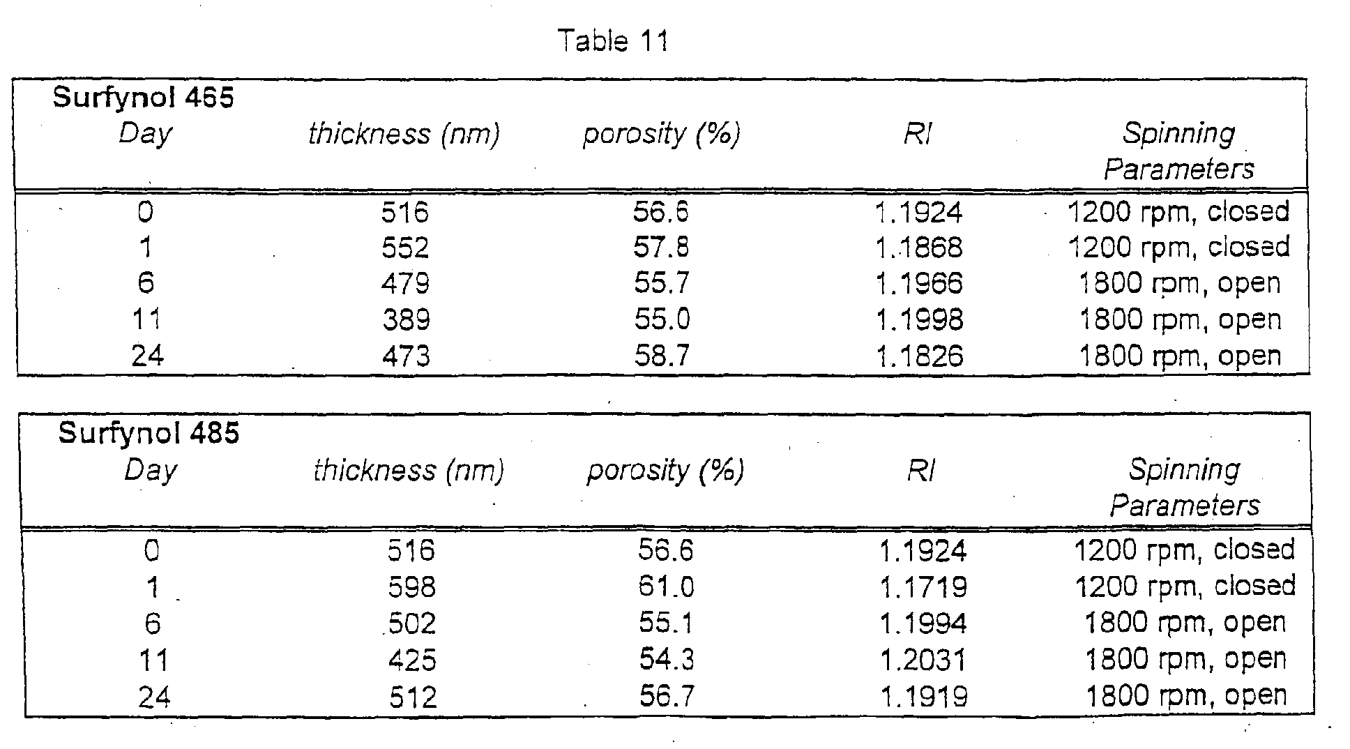
- the spinning solution requires 8.8 g of the stock solution prepared above, 12.5 g ethanol, 0.4 g water, 1 g 0.07 M HCI, and 2 g of surfactant, Surfynol 465 and Surfynol 485.
- the solution is then sonicated for 20 minutes and filtered through a 0.2 micron Acrodisc.
- the solution are then dispensed onto wafers and spun to dryness. After the wafers are prepared the surfactant is removed using thermal decomposition at 425°C in N 2 .
- the results from these solution for both the Surfynol 465 and Surfynol 485 are shown in Table 11.
- Example 33 Lower concentrations of ethoxylated acetylenic diols.
- This example shows the effects of lowering the surfactant concentration on the film properties.
- the same procedure as Example 32 was used except that th e amount of Surfynol 465 was decreased from the original 8 wt% (2.0 g) in the formulation to 4% (1.0 g) and 2% (0.5 g). All of wafers were spun in an open bowl configuration at 1800 r.pm. for 20 seconds and then calcined at 425°C in N 2 to remove the surfactant. Results are in Table 12, below. Weight % Surfynol 465 thickness (nm) porosity (%) RI 8 434 57.7 1.1872 4 358 35.8 1.2906 2 291 14.8 1.3907
- Example 34 Ethoxylated acetylenic diols and Oxalic acid.
- This example shows the use of oxalic acid in place of the HCI.
- the preparation replaces the 0.07 M HCI in the spinning solution and stock solution with 0.1 M oxalic acid using the same weighed amounts of each reagent.
- the solutions are mixed, sonicated, and filtered through a 0.2 micron Acrodisc before being spun onto a wafer.
- the wafers were spun in an open bowl configuration at 1800 r.p.m. for 20 seconds to remove excess solution and solvent and then calcined at 425°C in N2 to remove the surfactant from the film. Results are reported in Table 13, below.
- Example 35 Purity analysis of Surfactants.
- Example 36 Pore size determination.
- This example shows the pore sizes of the resulting films using the Surfynol surfactants from the preparations in the first example after calcination.
- the following Table 15 shows that the Surfynols give much smaller pore sizes, as measured using the SAW technique, than the block co-polymers, yet still have the porosity and refractive index similar to the mesoporous films.
- MTES methyltriethoxysilane
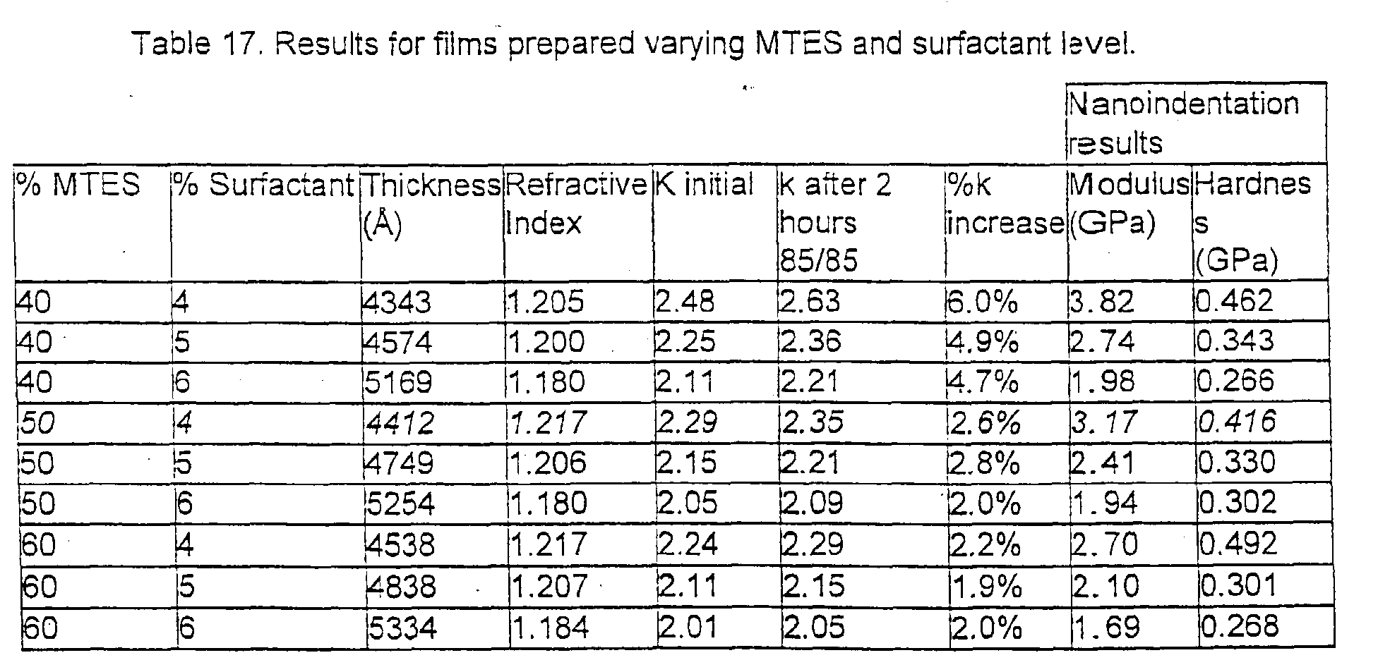
- Triton X-114 surfactant were varied to determine an optimum combination of low dielectric constant (k), k stability (using an 85°C / 85% relative humidity (85/85) test after 2 hours), and high modulus.
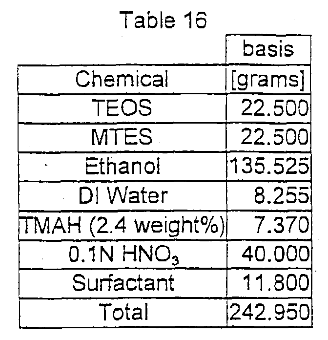
- the solutions were prepared using as a basis the following formulation. This formulation is described as a 50% MTES / 5% surfactant formulation as 50 weight % of the silica source is MTES and the surfactant is added at 5 weight % of the total formulation weight.
- All films were spun onto 8" wafers and processed using the same anneal process (air cure at 90, 180 and 400°C for 1.5, 1.5 and 3 minutes, respectively). The films were further thermally processed at 425°C for 6 minutes in a reduced pressure of N 2 .
Landscapes
- Chemical & Material Sciences (AREA)
- Chemical Kinetics & Catalysis (AREA)
- Organic Chemistry (AREA)
- Health & Medical Sciences (AREA)
- Medicinal Chemistry (AREA)
- Polymers & Plastics (AREA)
- Life Sciences & Earth Sciences (AREA)
- Engineering & Computer Science (AREA)
- Materials Engineering (AREA)
- Wood Science & Technology (AREA)
- Compositions Of Oxide Ceramics (AREA)
- Manufacture Of Macromolecular Shaped Articles (AREA)
- Formation Of Insulating Films (AREA)
- Paints Or Removers (AREA)
- Inorganic Insulating Materials (AREA)
- Production Of Multi-Layered Print Wiring Board (AREA)
- Silicon Compounds (AREA)
- Fixed Capacitors And Capacitor Manufacturing Machines (AREA)
- Chemically Coating (AREA)
- Laminated Bodies (AREA)
Abstract
Description
| Acid | Acetic | Acetic | HCI | HCI |
| Stored | Cold | Room Temp | Cold | Room Temp |
| Porosity (%) | ||||
| Days Old | Example 14 | Example 14 | Example 2 | Example 2 |
| 1 | 40.7 | 50.5. | 61.0 | 57.4 |
| 2 | 48.7 | 55.8 | 59.9 | 56.2 |
| 3 | 35.6 | 40.3 | 52.5 | 35.3 |
| 8 | 51.3 | 37.5 | 54.0 | 37.7 |
| 10 | 56.6 | 46.1 | 55.4 | 49.1 |
| 14 | 53.5 | 32.0 | 50.2 | 38.5 |
| 21 | 57.9 | 48.3 | 56.7 | 53.6 |
| 4% Brij 56 | 6% Brij 56 | 8% Brij 56 | 10% Brij 56 | 12% Brij 56 | |
| 20% PTES | 35.1 | ||||
| 35% PTES | 34.6 | ||||
| 5% TFTS | 41.9 | 49.8 | 50.7 | 51.2 | |
| 20% TFTS | 53.4 | 52.8 | 54.6 | 52.1 |
| 2 | 4 | 6 | 8 | 10 | |
| 20% PTES | 23.7 | 43.5 | |||
| 35 | |||||
| 5% TFTS | 42.6 | 56.1 | 58.7 | ||
| 20% TFTS | 49.0 | 51.5 | 55.4 | Film failure |
| 4 | 6 | 8 | |
| 20 | |||
| 35 | |||
| 5% TFTS | 59.1 | 59.2 | |
| 20% TFTS | 52.5 | 58.8 |
| Film | Void Fraction | Measured κ | Predicted |
| 5% TFTS / 8% Brij 56 | 0.471 | 2.45 | 2.46 |
| 5% TFTS / 6% P123 | 0.480 | 2.46 | 2.43 |
| 5% PTMS / 8% P123 | 0.290 | 2.93 | 3.07 |
| 5% TFTS / 6% P123 | 0.498 | 2.31 | 2.37 |
| 5% TFTS / 6% L121 | 0.507 | 2.19 | 2.35 |
| Solution Number | Surfactant | Weight percent in formulation |
| 1 | | 4% |
| 2 | | 6% |
| 3 | | 8% |
| 4 | | 10% |
| 5 | P123 | 4% |
| 6 | P123 | 6% |
| 7 | P123 | 8% |
| 8 | P123 | 10% |
| 9 | | 4% |
| 10 | | 6% |
| 11 | | 8% |
| 12 | Brij58 | 10% |
| 13 | | 4% |
| 14 | | 6% |
| 15 | | 8% |
| 16 | Brij56 | 10% |
| 17 | | 4% |
| 18 | | 6% |
| 19 | | 8% |
| 20 | | 10% |
| Number | Median Pore Size (Å) - SAW | RI | Percent Porosity (Ellipsometry) | Thickness(nm) |
| 1 | -- | 1.235 | 48.3% | 370 |
| 2 | 37 | 1.187 | 58.5% | 450 |
| 3 | 40 | 1.173 | 61.4% | 450 |
| 4 | 44 | 1.166 | 63.0% | 450 |
| 5 | -- | 1.248 | 46.0% | 370 |
| 6 | 37 | 1.174 | 61.0% | 460 |
| 7 | -- | 1.195 | 56.8% | 517 |
| 8 | -- | 1.372 | 20.1 % | 333 |
| 9 | -- | 1.277 | 39.7% | 275 |
| 10 | -- | 1.236 | 48.2% | 293 |
| 11 | -- | 1.226 | 50.4% | 288 |
| 12 | 40 | 1.219 | 52.0% | 310 |
| 13 | --- | 1.249 | 45.6% | 273 |
| 14 | --- | 1.237 | 48.1 % | 276 |
| 15 | -- | 1.234 | 48.7% | 258 |
| 16 | -- | 1.228 | 50.0% | 273 |
| 17 | -- | -- | -- | --- |
| 18 | -- | -- | - | --- |
| 19 | -- | - | --- | --- |
| 20 | - | -- | -- | --- |
| Number | Alcohol | Days old | HMDS | Median Pore Size (Å) - SAW | κ | RI | Percent Porosity (Ellipsometry) | Thickness(nm) |
| 23 | | 5 | No | --- | --- | 1.093 | 78.8% | 690 |
| 24 | | 5 | No | --- | --- | 1.147 | 67.0% | 615 |
| 25 | t- | 5 | No | --- | --- | 1.133 | 70.0% | 328 |
| 23 | isopropanol | 7 | No | 56 | 2.70 | 1.144 | 67.6% | 705 (675) |
| 24 | isobutanol | 7 | No | 69 | 2.63 | 1.155 | 65.2% | 651 (626) |
| 25 | t-butanol | 7 | No | 88 | --- | 1.137 | 69.1% | 373 |
| 26-1 | isopropanol | 7 | Yes | --- | 2.12 | 1.1-52 | 65.9% | 709 (645) |
| 26-1 | isobutanol | 7 | Yes | --- | 2.08 | 1.168 | 62.6% | 653 (619) |
| Number | Days old | RI | Percent Porosity | Thickness (nm) |
| HOAc heated | 0 | 1.2112 | 52.6 | 140 |
| HOAc room temp. | 0 | 1.2698 | 40.2 | 33.3 |
| HCI heated | 0 | 1.1995 | 55.1 | 770 |
| HCI room temp. | 0 | --- | --- | --- |
| HOAc heated | 1 | 1.1817 | 58.9 | 193 |
| HOAc room temp. | 1 | 1.2102 | 52.8 | 98.0 |
| HCI heated | 1 | 1.1924 | 56.6 | 726 |
| HCI room temp. | 1 | 1.1692 | 61.6 | 792 |
| HOAc heated | 7 | 1.1566 | 64.3 | 489 |
| HOAc room temp. | 7 | 1.1589 | 63.8 | 431 |
| HCI heated | 7 | 1.1919 | 56.7 | 717 |
| HCI room temp. | 7 | 1.1844 | 58.3 | 729 |
| Age of Oxalic Acid Sol (days) | RI | Percent Porosity | Thickness (nm) |
| 2 | 1.3894 | 16.6 | 430 |
| 3 | 1.1680 | 62.5 | 800 |
| 4 | 1.1731 | 61.4 | 811 |
| 7 | 1.1950 | 56.8 | 826 |
| 8 | 1.2026 | 55.2 | 710 |
| 14 | 1.2040 | 54.9 | 777 |
| Weight % Surfynol 465 | thickness (nm) | porosity (%) | |
| 8 | 434 | 57.7 | 1.1872 |
| 4 | 358 | 35.8 | 1.2906 |
| 2 | 291 | 14.8 | 1.3907 |
| Surfactant | thickness (nm) | porosity (%) | RI |
| Surfynol 465 | 403 | 51.4 | 1.2167 |
| Surfynol 485 | 405 | 57.7 | 1.1872 |
| Surfactant | ppm Na | ppm K |
| Triton X-114 | 427.6 | 1.0 |
| BASF L121 | 2.6 | 483.1 |
| BASF L101 | 0.24 | 1.9 |
| Surfynol 465 | 0.18 | 0.81 |
| Surfynol 485 | 0.19 | 0.85 |
| Surfactant | Median Pore Diameter (Å) | Average Pore Diameter (Å) |
| | 50 | 43 |
| BASF L101 | 41 | 37 |
| Surfynol 465 | 29 | 29 |
| Surfynol 485 | 29 | 29 |
Claims (29)
- A process for producing a ceramic film on a substrate, said process comprising:wherein said ceramic film has a dielectric constant below 2.3, and a metal content of less than 500 ppm.preparing a film-forming fluid comprising a ceramic precursor, a catalyst, a surfactant and solvent(s);depositing said film-forming fluid on said substrate; andremoving said solvent(s) from said film-forming fluid on said substrate to produce said ceramic film on said substrate,
- The method of claim 1, wherein said dielectric constant is from 2.2 to 1.3.
- The method of claim 1, wherein said halide content is less than 1 ppm.
- The method of claim 3, wherein said halide content is less than 500 ppb and said metal content is less than 1 ppm.
- The method of claim 1, wherein said metal content is less than 1 ppm.
- The method of claim 1, wherein said metal content is less than 100 ppb.
- The method of claim 1, wherein said ceramic precursor is selected from the group consisting of tetraethoxysilane, tetramethoxysilane, titanium (IV) isopropoxide, titanium (IV) methoxide and aluminum sec-butoxide.
- The method of claim 1, wherein said ceramic precursor is an alkylalkoxysilane, which provides improved k stability, maintains low k value and maintains high modulus.
- The method of claim 1, wherein said catalyst is an organic acid and said film-forming fluid is free of HCI, HBr, H2SO4, and H3PO4 acid catalysts.
- The method of claim 1, wherein said catalyst is selected from the group consisting of acetic acid, formic acid, glycolic acid, glyoxylic acid, oxalic acid and HNO3.
- The method of claim 1, wherein said surfactant is nonionic and said film-forming fluid is free of ionic surfactants.
- The method of claim 1, wherein said surfactant is a block copolymer of ethylene oxide and propylene oxide.
- The method of claim 1, wherein said surfactant is selected from the group consisting of block copolymers of ethylene oxide and propylene oxide and polyoxyethylene alkyl ethers.
- The method of claim 1, wherein said surfactant is an ethoxylated acetylenic diol.
- The method of claim 1, wherein said surfactant is an octylphenol ethoxylates.
- The method of claim 1, wherein said solvent is selected from the group consisting of methanol, isopropanol, isobutanol, ethanol and n-butanol.
- The method of claim 1, wherein said solvent removing comprises spinning said substrate and calcining said ceramic film on said substrate.
- The method of claim 1, wherein said film-forming fluid is a sol having a gelation time of at least 300 hours.
- The method of claim 1, wherein said ceramic film has a porosity of about 50% to about 85%.
- A ceramic film produced by the process of claim 1.
- The ceramic film of claim 20, wherein said dielectric constant is from 2.2 to 1.3.
- The ceramic film of claim 20, wherein said halide content is less than 500 ppb.
- The ceramic film of claim 20, wherein said metal content is less than 1 ppm.
- The ceramic film of claim 20, wherein said metal content is less than 100 ppb.
- The ceramic film of claim 20, having a porosity of about 50% to about 80%.
- The ceramic film of claim 20, having a porosity of about 55% to about 75%.
- The ceramic film of claim 20, wherein said film includes pores sufficiently ordered in a plane of the substrate that an X-ray diffraction pattern of said film shows a Bragg diffraction at a d spacing greater than about 44 Å.
- The ceramic film of claim 20, wherein said film does not include pores sufficiently ordered in a plane of the substrate such that an X-ray diffraction pattern of said film shows a Bragg diffraction.
- A ceramic film produced by the process of claim 1 wherein said ceramic precursor is an alkylalkoxysilane, which provides improved k stability, maintains low k value and maintains high modulus.
Applications Claiming Priority (6)
| Application Number | Priority Date | Filing Date | Title |
|---|---|---|---|
| US711573 | 1996-09-10 | ||
| US45599999A | 1999-12-07 | 1999-12-07 | |
| US455999 | 1999-12-07 | ||
| US518955 | 2000-03-03 | ||
| US09/518,955 US6365266B1 (en) | 1999-12-07 | 2000-03-03 | Mesoporous films having reduced dielectric constants |
| US09/711,573 US6592980B1 (en) | 1999-12-07 | 2000-11-13 | Mesoporous films having reduced dielectric constants |
Publications (3)
| Publication Number | Publication Date |
|---|---|
| EP1123753A2 true EP1123753A2 (en) | 2001-08-16 |
| EP1123753A3 EP1123753A3 (en) | 2004-04-28 |
| EP1123753B1 EP1123753B1 (en) | 2007-08-29 |
Family
ID=27412650
Family Applications (1)
| Application Number | Title | Priority Date | Filing Date |
|---|---|---|---|
| EP20000126445 Expired - Lifetime EP1123753B1 (en) | 1999-12-07 | 2000-12-06 | Mesoporous ceramic films having reduced dielectric constants |
Country Status (8)
| Country | Link |
|---|---|
| US (2) | US6592980B1 (en) |
| EP (1) | EP1123753B1 (en) |
| JP (1) | JP3668126B2 (en) |
| KR (1) | KR100412312B1 (en) |
| AT (1) | ATE371952T1 (en) |
| DE (1) | DE60036191T2 (en) |
| IL (1) | IL140057A0 (en) |
| TW (1) | TW581713B (en) |
Cited By (18)
| Publication number | Priority date | Publication date | Assignee | Title |
|---|---|---|---|---|
| EP1376671A1 (en) * | 2002-05-30 | 2004-01-02 | Air Products And Chemicals, Inc. | Compositions for preparing materials with a low dielectric constant |
| US6818289B2 (en) * | 1999-12-07 | 2004-11-16 | Air Products And Chemicals, Inc. | Mesoporous films having reduced dielectric constants |
| SG113504A1 (en) * | 2003-04-01 | 2005-08-29 | Air Prod & Chem | Low dielectric materials and methods for making same |
| US6946161B2 (en) * | 2002-08-27 | 2005-09-20 | Ulvac, Inc. | Method for forming porous silica film |
| EP1580804A4 (en) * | 2002-11-13 | 2006-01-25 | Matsushita Electric Industrial Co Ltd | COMPOSITION FOR POROUS FILM FORMATION, POROUS FILMS, PROCESS FOR PRODUCING POROUS FILMS, DIELECTRIC INTERLAYERS, AND SEMICONDUCTOR DEVICES |
| US7001669B2 (en) | 2002-12-23 | 2006-02-21 | The Administration Of The Tulane Educational Fund | Process for the preparation of metal-containing nanostructured films |
| US7119354B2 (en) | 2003-04-09 | 2006-10-10 | Shin-Etsu Chemical Co., Ltd. | Composition for forming porous film, porous film and method for forming the same, interlevel insulator film |
| US7132473B2 (en) | 2002-11-13 | 2006-11-07 | Matsushita Electric Industrial Co., Ltd. | Composition for forming porous film, porous film and method for forming the same, interlevel insulator film, and semiconductor device |
| WO2007012890A1 (en) * | 2005-07-26 | 2007-02-01 | Compactgtl Plc | Catalyst |
| US7186613B2 (en) | 2002-05-30 | 2007-03-06 | Air Products And Chemicals, Inc. | Low dielectric materials and methods for making same |
| US7205338B2 (en) | 2003-03-10 | 2007-04-17 | Shin-Etsu Chemical Co., Ltd. | Composition for forming porous film, porous film and method for forming the same, interlevel insulator film, and semiconductor device |
| US7332446B2 (en) | 2003-03-27 | 2008-02-19 | Shin-Etsu Chemical Co., Ltd. | Composition for forming porous film, porous film and method for forming the same, interlevel insulator film and semiconductor device |
| US7357961B2 (en) | 2003-04-09 | 2008-04-15 | Matsushita Electric Industrial Co., Ltd. | Composition for forming porous film, porous film and method for forming the same, interlevel insulator film, and semiconductor device |
| US7897119B2 (en) | 2006-05-08 | 2011-03-01 | Compactgtl Plc | Catalytic reactor |
| EP2306499A2 (en) | 2002-11-14 | 2011-04-06 | Air Products and Chemicals, Inc. | Non-thermal process for forming porous low dielectric constant films |
| US8231966B2 (en) | 2008-03-03 | 2012-07-31 | Keio University | Anti-reflection coating and its production method |
| EP3231892A1 (en) | 2003-03-04 | 2017-10-18 | Versum Materials US, LLC | Mechanical enhancement of dense and porous organosilicate materials by uv exposure |
| EP1520891B1 (en) * | 2003-09-25 | 2019-05-01 | JSR Corporation | Film forming composition, process for producing film forming composition, insulating film forming material, process for forming film, and silica-based film |
Families Citing this family (44)
| Publication number | Priority date | Publication date | Assignee | Title |
|---|---|---|---|---|
| US6576568B2 (en) * | 2000-04-04 | 2003-06-10 | Applied Materials, Inc. | Ionic additives for extreme low dielectric constant chemical formulations |
| US7265062B2 (en) * | 2000-04-04 | 2007-09-04 | Applied Materials, Inc. | Ionic additives for extreme low dielectric constant chemical formulations |
| JP4972834B2 (en) * | 2001-08-28 | 2012-07-11 | 日立化成工業株式会社 | Siloxane resin |
| JP2003064307A (en) * | 2001-08-28 | 2003-03-05 | Hitachi Chem Co Ltd | Silica-based film, composition for forming silica-based film, method for producing silica-based film and electronic part |
| EP1502154B1 (en) * | 2001-12-17 | 2009-02-18 | Northwestern University | Patterning of solid state features by direct write nanolithographic printing |
| CN1218634C (en) * | 2002-04-30 | 2005-09-14 | 香港中文大学 | Preparation method of mesoporous titanium dioxide film with high bactericidal photoactivity |
| JP3939612B2 (en) * | 2002-08-12 | 2007-07-04 | 株式会社豊田中央研究所 | Road friction estimation device |
| JP4056347B2 (en) * | 2002-09-30 | 2008-03-05 | ローム株式会社 | Semiconductor light emitting device and manufacturing method thereof |
| JP2004161877A (en) * | 2002-11-13 | 2004-06-10 | Shin Etsu Chem Co Ltd | Composition for forming porous film, porous film and manufacturing method thereof, interlayer insulating film, and semiconductor device |
| JP2004161876A (en) * | 2002-11-13 | 2004-06-10 | Shin Etsu Chem Co Ltd | Composition for forming porous film, porous film and manufacturing method thereof, interlayer insulating film, and semiconductor device |
| JP2004307693A (en) * | 2003-04-09 | 2004-11-04 | Shin Etsu Chem Co Ltd | Composition for forming porous film, method for producing porous film, porous film, interlayer insulating film, and semiconductor device |
| CA2534924A1 (en) * | 2003-08-08 | 2005-02-24 | Elan Pharma International Ltd. | Novel metaxalone compositions |
| US7445814B2 (en) * | 2003-10-22 | 2008-11-04 | Hewlett-Packard Development Company, L.P. | Methods of making porous cermet and ceramic films |
| US8097269B2 (en) * | 2004-02-18 | 2012-01-17 | Celonova Biosciences, Inc. | Bioactive material delivery systems comprising sol-gel compositions |
| WO2005082277A1 (en) * | 2004-02-18 | 2005-09-09 | Stanford University | Drug delivery systems using mesoporous oxide films |
| FR2874007B1 (en) | 2004-08-03 | 2007-11-23 | Essilor Int | PROCESS FOR PRODUCING A SUBSTRATE COATED WITH A MESOPOROUS LAYER AND ITS OPTICAL APPLICATION |
| US8901268B2 (en) | 2004-08-03 | 2014-12-02 | Ahila Krishnamoorthy | Compositions, layers and films for optoelectronic devices, methods of production and uses thereof |
| US20060183055A1 (en) * | 2005-02-15 | 2006-08-17 | O'neill Mark L | Method for defining a feature on a substrate |
| US7446055B2 (en) * | 2005-03-17 | 2008-11-04 | Air Products And Chemicals, Inc. | Aerosol misted deposition of low dielectric organosilicate films |
| JP4894153B2 (en) * | 2005-03-23 | 2012-03-14 | 株式会社アルバック | Precursor composition of porous film and preparation method thereof, porous film and preparation method thereof, and semiconductor device |
| US20060220251A1 (en) * | 2005-03-31 | 2006-10-05 | Grant Kloster | Reducing internal film stress in dielectric film |
| JP2006315943A (en) * | 2005-04-14 | 2006-11-24 | Sumitomo Chemical Co Ltd | Manufacturing method of ceramic sintered body |
| FR2896887B1 (en) * | 2006-02-02 | 2008-05-30 | Essilor Int | ARTICLE COMPRISING A MESOPOROUS COATING HAVING A REFRACTIVE INDEX PROFILE AND METHODS OF MAKING THE SAME |
| US8399349B2 (en) | 2006-04-18 | 2013-03-19 | Air Products And Chemicals, Inc. | Materials and methods of forming controlled void |
| JP5030478B2 (en) | 2006-06-02 | 2012-09-19 | 株式会社アルバック | Precursor composition of porous film and preparation method thereof, porous film and preparation method thereof, and semiconductor device |
| WO2008041383A1 (en) * | 2006-09-29 | 2008-04-10 | Nippon Tungsten Co., Ltd. | Substrate material for magnetic head and method for manufacturing the same |
| WO2008080096A2 (en) * | 2006-12-21 | 2008-07-03 | Advanced Technology Materials, Inc. | Compositions and methods for the selective removal of silicon nitride |
| CN102351201B (en) | 2007-03-13 | 2013-07-31 | 三菱化学株式会社 | Porous silica body, layered body and composition for optical use, and method for producing porous silica body |
| US9114125B2 (en) | 2008-04-11 | 2015-08-25 | Celonova Biosciences, Inc. | Drug eluting expandable devices |
| JP5004866B2 (en) * | 2008-05-15 | 2012-08-22 | 旭化成株式会社 | Thin film for interlayer insulation |
| US20100151206A1 (en) | 2008-12-11 | 2010-06-17 | Air Products And Chemicals, Inc. | Method for Removal of Carbon From An Organosilicate Material |
| CN102307935B (en) * | 2008-12-23 | 2017-06-09 | 3M创新有限公司 | Amorphous microporous organosilicate compositions |
| US8647884B2 (en) | 2008-12-23 | 2014-02-11 | 3M Innovative Properties Company | Organic chemical sensor with microporous organosilicate material |
| BRPI0918200A2 (en) | 2008-12-23 | 2015-12-08 | 3M Innovative Properties Co | detection element and method of detection of organic chemical analytes |
| US8557877B2 (en) | 2009-06-10 | 2013-10-15 | Honeywell International Inc. | Anti-reflective coatings for optically transparent substrates |
| CN102471590B (en) | 2009-07-14 | 2015-05-20 | 花王株式会社 | Low-permittivity resin composition |
| FR2949111B1 (en) | 2009-08-13 | 2013-03-22 | Essilor Int | METHOD FOR MANUFACTURING A MESOPOROUS ANTISTATIC FILM-COATED SUBSTRATE AND ITS APPLICATION IN OPTICAL OPTICS |
| KR101044957B1 (en) * | 2009-09-16 | 2011-06-28 | 도레이첨단소재 주식회사 | Water Disperse Silicone Release Liquid and Polyester Release Film Using the Same |
| FR2965820B1 (en) | 2010-10-12 | 2012-11-16 | Essilor Int | ARTICLE COMPRISING A MESOPOROUS LAYER PROTECTED BY A SEBUM BARRIER COATING AND METHOD OF MANUFACTURE |
| US8864898B2 (en) | 2011-05-31 | 2014-10-21 | Honeywell International Inc. | Coating formulations for optical elements |
| JP6285095B2 (en) * | 2012-09-28 | 2018-02-28 | 日立化成株式会社 | Composition for forming semiconductor substrate passivation film, semiconductor substrate with passivation film and method for producing the same, solar cell element and method for producing the same |
| WO2014175124A1 (en) * | 2013-04-24 | 2014-10-30 | 旭硝子株式会社 | Substrate having antireflective layer |
| US10170297B2 (en) * | 2013-08-22 | 2019-01-01 | Versum Materials Us, Llc | Compositions and methods using same for flowable oxide deposition |
| US10544329B2 (en) | 2015-04-13 | 2020-01-28 | Honeywell International Inc. | Polysiloxane formulations and coatings for optoelectronic applications |
Family Cites Families (35)
| Publication number | Priority date | Publication date | Assignee | Title |
|---|---|---|---|---|
| US2692838A (en) * | 1951-05-26 | 1954-10-26 | Bell Telephone Labor Inc | Process for producing a silica coating |
| US3594081A (en) * | 1968-11-04 | 1971-07-20 | Werner Tschink | Adjustable illuminating device |
| US4010133A (en) * | 1971-05-26 | 1977-03-01 | E. I. Du Pont De Nemours And Company | Low-fire green ceramic articles and slip compositions for producing same |
| US4142004A (en) * | 1976-01-22 | 1979-02-27 | Bell Telephone Laboratories, Incorporated | Method of coating semiconductor substrates |
| US4271210A (en) * | 1979-10-25 | 1981-06-02 | Westinghouse Electric Corp. | Method of forming transmissive, porous metal oxide optical layer of a vitreous substrate |
| US5605628A (en) * | 1988-05-24 | 1997-02-25 | North West Water Group Plc | Composite membranes |
| JPH082511B2 (en) * | 1989-05-08 | 1996-01-17 | 松下電器産業株式会社 | Laser processing equipment |
| US5021398A (en) * | 1989-10-26 | 1991-06-04 | Amp Incorporated | Method of forming patterned oxide superconducting films |
| US5302798A (en) * | 1991-04-01 | 1994-04-12 | Canon Kabushiki Kaisha | Method of forming a hole with a laser and an apparatus for forming a hole with a laser |
| FR2707763B1 (en) * | 1993-07-16 | 1995-08-11 | Commissariat Energie Atomique | Composite material with a high refractive index, process for manufacturing this composite material and optically active material comprising this composite material. |
| US5645891A (en) | 1994-11-23 | 1997-07-08 | Battelle Memorial Institute | Ceramic porous material and method of making same |
| EP0775669B1 (en) * | 1995-11-16 | 2001-05-02 | Texas Instruments Incorporated | Low volatility solvent-based precursors for nanoporous aerogels |
| US6063714A (en) | 1995-11-16 | 2000-05-16 | Texas Instruments Incorporated | Nanoporous dielectric thin film surface modification |
| US5889449A (en) * | 1995-12-07 | 1999-03-30 | Space Systems/Loral, Inc. | Electromagnetic transmission line elements having a boundary between materials of high and low dielectric constants |
| DE19707834A1 (en) * | 1996-04-09 | 1997-10-16 | Zeiss Carl Fa | Material irradiation unit used e.g. in production of circuit boards |
| US5750641A (en) * | 1996-05-23 | 1998-05-12 | Minnesota Mining And Manufacturing Company | Polyimide angularity enhancement layer |
| US5922299A (en) * | 1996-11-26 | 1999-07-13 | Battelle Memorial Institute | Mesoporous-silica films, fibers, and powders by evaporation |
| JP4011120B2 (en) * | 1996-12-27 | 2007-11-21 | Azエレクトロニックマテリアルズ株式会社 | Polyorganosiloxazan and process for producing the same |
| US5973290A (en) * | 1997-02-26 | 1999-10-26 | W. L. Gore & Associates, Inc. | Laser apparatus having improved via processing rate |
| US6211096B1 (en) * | 1997-03-21 | 2001-04-03 | Lsi Logic Corporation | Tunable dielectric constant oxide and method of manufacture |
| US5858457A (en) | 1997-09-25 | 1999-01-12 | Sandia Corporation | Process to form mesostructured films |
| US6120891A (en) * | 1997-10-29 | 2000-09-19 | Board Of Regemts. The University Of Texas System | Mesoporous transition metal oxide thin films and methods of making and uses thereof |
| WO1999037705A1 (en) | 1997-12-09 | 1999-07-29 | The Regents Of The University Of California | Block polymer processing for mesostructured inorganic oxide materials |
| US6027666A (en) * | 1998-06-05 | 2000-02-22 | The Governing Council Of The University Of Toronto | Fast luminescent silicon |
| US6395651B1 (en) * | 1998-07-07 | 2002-05-28 | Alliedsignal | Simplified process for producing nanoporous silica |
| JP3003684B1 (en) * | 1998-09-07 | 2000-01-31 | 日本電気株式会社 | Substrate cleaning method and substrate cleaning liquid |
| FR2787350B1 (en) | 1998-12-21 | 2002-01-04 | Saint Gobain Vitrage | GLASS WITH FUNCTIONAL MESOPOROUS COATING, ESPECIALLY HYDROPHOBIC |
| IL143589A0 (en) | 1998-12-23 | 2002-04-21 | Battelle Memorial Institute | Mesoporous silica film from a solution containing a surfactant and methods of making same |
| US6197913B1 (en) * | 1999-08-26 | 2001-03-06 | Dow Corning Corporation | Method for making microporous silicone resins with narrow pore-size distributions |
| DE60025959T2 (en) * | 1999-11-22 | 2006-10-19 | Jsr Corp. | Composite particles and aqueous dispersions for chemical mechanical polishing |
| US6365266B1 (en) * | 1999-12-07 | 2002-04-02 | Air Products And Chemicals, Inc. | Mesoporous films having reduced dielectric constants |
| US6592980B1 (en) * | 1999-12-07 | 2003-07-15 | Air Products And Chemicals, Inc. | Mesoporous films having reduced dielectric constants |
| TW572980B (en) * | 2000-01-12 | 2004-01-21 | Jsr Corp | Aqueous dispersion for chemical mechanical polishing and chemical mechanical polishing process |
| US6576568B2 (en) * | 2000-04-04 | 2003-06-10 | Applied Materials, Inc. | Ionic additives for extreme low dielectric constant chemical formulations |
| JP2001291427A (en) * | 2000-04-06 | 2001-10-19 | Dow Corning Toray Silicone Co Ltd | Electrically insulating thin film-forming resin composition and method for forming electrically insulating thin film |
-
2000
- 2000-11-13 US US09/711,573 patent/US6592980B1/en not_active Expired - Fee Related
- 2000-12-04 IL IL14005700A patent/IL140057A0/en not_active IP Right Cessation
- 2000-12-06 EP EP20000126445 patent/EP1123753B1/en not_active Expired - Lifetime
- 2000-12-06 AT AT00126445T patent/ATE371952T1/en not_active IP Right Cessation
- 2000-12-06 DE DE2000636191 patent/DE60036191T2/en not_active Expired - Fee Related
- 2000-12-07 KR KR10-2000-0074303A patent/KR100412312B1/en not_active Expired - Fee Related
- 2000-12-07 JP JP2000372712A patent/JP3668126B2/en not_active Expired - Fee Related
-
2001
- 2001-06-04 TW TW89125832A patent/TW581713B/en not_active IP Right Cessation
-
2002
- 2002-10-02 US US10/263,254 patent/US6818289B2/en not_active Expired - Fee Related
Cited By (27)
| Publication number | Priority date | Publication date | Assignee | Title |
|---|---|---|---|---|
| US6818289B2 (en) * | 1999-12-07 | 2004-11-16 | Air Products And Chemicals, Inc. | Mesoporous films having reduced dielectric constants |
| EP1852903A3 (en) * | 2002-05-30 | 2008-12-10 | Air Products and Chemicals, Inc. | Compositions for preparing materials with a low dielectric constant |
| US7307343B2 (en) | 2002-05-30 | 2007-12-11 | Air Products And Chemicals, Inc. | Low dielectric materials and methods for making same |
| EP1376671A1 (en) * | 2002-05-30 | 2004-01-02 | Air Products And Chemicals, Inc. | Compositions for preparing materials with a low dielectric constant |
| US7482676B2 (en) | 2002-05-30 | 2009-01-27 | Air Products And Chemicals, Inc. | Compositions for preparing low dielectric materials |
| US7294585B2 (en) * | 2002-05-30 | 2007-11-13 | Air Products And Chemicals, Inc. | Compositions for preparing low dielectric materials |
| US7186613B2 (en) | 2002-05-30 | 2007-03-06 | Air Products And Chemicals, Inc. | Low dielectric materials and methods for making same |
| US7122880B2 (en) | 2002-05-30 | 2006-10-17 | Air Products And Chemicals, Inc. | Compositions for preparing low dielectric materials |
| US6946161B2 (en) * | 2002-08-27 | 2005-09-20 | Ulvac, Inc. | Method for forming porous silica film |
| EP1580804A4 (en) * | 2002-11-13 | 2006-01-25 | Matsushita Electric Industrial Co Ltd | COMPOSITION FOR POROUS FILM FORMATION, POROUS FILMS, PROCESS FOR PRODUCING POROUS FILMS, DIELECTRIC INTERLAYERS, AND SEMICONDUCTOR DEVICES |
| US7341775B2 (en) | 2002-11-13 | 2008-03-11 | Matsushita Electric Industrial Co. Ltd. | Composition for forming porous film, porous film and method for forming the same, interlevel insulator film, and semiconductor device |
| US7132473B2 (en) | 2002-11-13 | 2006-11-07 | Matsushita Electric Industrial Co., Ltd. | Composition for forming porous film, porous film and method for forming the same, interlevel insulator film, and semiconductor device |
| EP2306499A2 (en) | 2002-11-14 | 2011-04-06 | Air Products and Chemicals, Inc. | Non-thermal process for forming porous low dielectric constant films |
| US7001669B2 (en) | 2002-12-23 | 2006-02-21 | The Administration Of The Tulane Educational Fund | Process for the preparation of metal-containing nanostructured films |
| EP3231892A1 (en) | 2003-03-04 | 2017-10-18 | Versum Materials US, LLC | Mechanical enhancement of dense and porous organosilicate materials by uv exposure |
| US7205338B2 (en) | 2003-03-10 | 2007-04-17 | Shin-Etsu Chemical Co., Ltd. | Composition for forming porous film, porous film and method for forming the same, interlevel insulator film, and semiconductor device |
| US7332446B2 (en) | 2003-03-27 | 2008-02-19 | Shin-Etsu Chemical Co., Ltd. | Composition for forming porous film, porous film and method for forming the same, interlevel insulator film and semiconductor device |
| SG113504A1 (en) * | 2003-04-01 | 2005-08-29 | Air Prod & Chem | Low dielectric materials and methods for making same |
| US7357961B2 (en) | 2003-04-09 | 2008-04-15 | Matsushita Electric Industrial Co., Ltd. | Composition for forming porous film, porous film and method for forming the same, interlevel insulator film, and semiconductor device |
| US7119354B2 (en) | 2003-04-09 | 2006-10-10 | Shin-Etsu Chemical Co., Ltd. | Composition for forming porous film, porous film and method for forming the same, interlevel insulator film |
| EP1520891B1 (en) * | 2003-09-25 | 2019-05-01 | JSR Corporation | Film forming composition, process for producing film forming composition, insulating film forming material, process for forming film, and silica-based film |
| US7985708B2 (en) | 2005-07-26 | 2011-07-26 | Compactgtl Plc | Methods of making and using a catalyst |
| GB2442363B (en) * | 2005-07-26 | 2009-06-17 | Compactgtl Plc | Catalyst |
| GB2442363A (en) * | 2005-07-26 | 2008-04-02 | Compactgtl Plc | Catalyst |
| WO2007012890A1 (en) * | 2005-07-26 | 2007-02-01 | Compactgtl Plc | Catalyst |
| US7897119B2 (en) | 2006-05-08 | 2011-03-01 | Compactgtl Plc | Catalytic reactor |
| US8231966B2 (en) | 2008-03-03 | 2012-07-31 | Keio University | Anti-reflection coating and its production method |
Also Published As
| Publication number | Publication date |
|---|---|
| US20030157311A1 (en) | 2003-08-21 |
| TW581713B (en) | 2004-04-01 |
| IL140057A0 (en) | 2002-02-10 |
| ATE371952T1 (en) | 2007-09-15 |
| US6592980B1 (en) | 2003-07-15 |
| KR100412312B1 (en) | 2003-12-31 |
| EP1123753A3 (en) | 2004-04-28 |
| DE60036191T2 (en) | 2007-12-27 |
| JP2001226171A (en) | 2001-08-21 |
| EP1123753B1 (en) | 2007-08-29 |
| US6818289B2 (en) | 2004-11-16 |
| KR20010062224A (en) | 2001-07-07 |
| DE60036191D1 (en) | 2007-10-11 |
| JP3668126B2 (en) | 2005-07-06 |
Similar Documents
| Publication | Publication Date | Title |
|---|---|---|
| US6818289B2 (en) | Mesoporous films having reduced dielectric constants | |
| US6365266B1 (en) | Mesoporous films having reduced dielectric constants | |
| De Theije et al. | Structural characterization of mesoporous organosilica films for ultralow-k dielectrics | |
| KR100536178B1 (en) | Mesoporous silica film from a solution containing a surfactant and methods of making same | |
| US7186613B2 (en) | Low dielectric materials and methods for making same | |
| US20060046079A1 (en) | Method for preparing surfactant-templated, mesoporous low dielectric film | |
| US6329017B1 (en) | Mesoporous silica film from a solution containing a surfactant and methods of making same | |
| US20040058079A1 (en) | Method for forming porous silica film | |
| US20070108593A1 (en) | Zeolite sol and method for preparing the same, composition for forming porous film, porous film and method for forming the same, interlevel insulator film, and semiconductor device | |
| US20090130412A1 (en) | Method of transformation of bridging organic groups in organosilica materials | |
| US7807267B2 (en) | Method of modifying porous film, modified porous film and use of same | |
| JP2005522878A (en) | Low metal porous silica dielectrics for integrated circuit applications | |
| JP5030478B2 (en) | Precursor composition of porous film and preparation method thereof, porous film and preparation method thereof, and semiconductor device | |
| Goethals et al. | Ultra-low-k cyclic carbon-bridged PMO films with a high chemical resistance | |
| US20070037411A1 (en) | Method of manufacturing an electronic device | |
| US20090208737A1 (en) | Lamella structured thin films with ultralow dielectric constants and high hardness and method for manufacturing the same | |
| Yu et al. | Surface modified silica mesoporous films as a low dielectric constant intermetal dielectric | |
| HK1037564B (en) | Mesoporous ceramic films having reduced dielectric constants | |
| Chao et al. | Preparation and characterization of low-k mesoporous silica films | |
| Chao et al. | PREPARATION AND CHARACTERIZATION OF |
Legal Events
| Date | Code | Title | Description |
|---|---|---|---|
| PUAI | Public reference made under article 153(3) epc to a published international application that has entered the european phase |
Free format text: ORIGINAL CODE: 0009012 |
|
| AK | Designated contracting states |
Kind code of ref document: A2 Designated state(s): AT BE CH CY DE DK ES FI FR GB GR IE IT LI LU MC NL PT SE TR |
|
| AX | Request for extension of the european patent |
Free format text: AL;LT;LV;MK;RO;SI |
|
| PUAL | Search report despatched |
Free format text: ORIGINAL CODE: 0009013 |
|
| AK | Designated contracting states |
Kind code of ref document: A3 Designated state(s): AT BE CH CY DE DK ES FI FR GB GR IE IT LI LU MC NL PT SE TR |
|
| AX | Request for extension of the european patent |
Extension state: AL LT LV MK RO SI |
|
| RIC1 | Information provided on ipc code assigned before grant |
Ipc: 7H 01L 21/316 A |
|
| 17P | Request for examination filed |
Effective date: 20040525 |
|
| 17Q | First examination report despatched |
Effective date: 20040721 |
|
| AKX | Designation fees paid |
Designated state(s): AT BE CH CY DE DK ES FI FR GB GR IE IT LI LU MC NL PT SE TR |
|
| GRAP | Despatch of communication of intention to grant a patent |
Free format text: ORIGINAL CODE: EPIDOSNIGR1 |
|
| GRAS | Grant fee paid |
Free format text: ORIGINAL CODE: EPIDOSNIGR3 |
|
| GRAA | (expected) grant |
Free format text: ORIGINAL CODE: 0009210 |
|
| AK | Designated contracting states |
Kind code of ref document: B1 Designated state(s): AT BE CH CY DE DK ES FI FR GB GR IE IT LI LU MC NL PT SE TR |
|
| REG | Reference to a national code |
Ref country code: GB Ref legal event code: FG4D |
|
| RIN1 | Information on inventor provided before grant (corrected) |
Inventor name: NAULT, MICHAEL P. Inventor name: BEKIARIS, NIKOLAOS Inventor name: MANDAL, ROBERT PARKASH Inventor name: MACDOUGALL, JAMES EDWARD Inventor name: WEIDMAN, TIMOTHY W. Inventor name: LU, YUNFENG Inventor name: WEIGEL, SCOTT JEFFREY Inventor name: HEIER, KEVIN R. Inventor name: DEMOS, ALEXANDROS T. |
|
| REG | Reference to a national code |
Ref country code: CH Ref legal event code: EP |
|
| REG | Reference to a national code |
Ref country code: IE Ref legal event code: FG4D |
|
| REF | Corresponds to: |
Ref document number: 60036191 Country of ref document: DE Date of ref document: 20071011 Kind code of ref document: P |
|
| PG25 | Lapsed in a contracting state [announced via postgrant information from national office to epo] |
Ref country code: ES Free format text: LAPSE BECAUSE OF FAILURE TO SUBMIT A TRANSLATION OF THE DESCRIPTION OR TO PAY THE FEE WITHIN THE PRESCRIBED TIME-LIMIT Effective date: 20071210 Ref country code: FI Free format text: LAPSE BECAUSE OF FAILURE TO SUBMIT A TRANSLATION OF THE DESCRIPTION OR TO PAY THE FEE WITHIN THE PRESCRIBED TIME-LIMIT Effective date: 20070829 |
|
| PG25 | Lapsed in a contracting state [announced via postgrant information from national office to epo] |
Ref country code: AT Free format text: LAPSE BECAUSE OF FAILURE TO SUBMIT A TRANSLATION OF THE DESCRIPTION OR TO PAY THE FEE WITHIN THE PRESCRIBED TIME-LIMIT Effective date: 20070829 Ref country code: LI Free format text: LAPSE BECAUSE OF FAILURE TO SUBMIT A TRANSLATION OF THE DESCRIPTION OR TO PAY THE FEE WITHIN THE PRESCRIBED TIME-LIMIT Effective date: 20070829 Ref country code: CH Free format text: LAPSE BECAUSE OF FAILURE TO SUBMIT A TRANSLATION OF THE DESCRIPTION OR TO PAY THE FEE WITHIN THE PRESCRIBED TIME-LIMIT Effective date: 20070829 |
|
| REG | Reference to a national code |
Ref country code: CH Ref legal event code: PL |
|
| ET | Fr: translation filed | ||
| PG25 | Lapsed in a contracting state [announced via postgrant information from national office to epo] |
Ref country code: BE Free format text: LAPSE BECAUSE OF FAILURE TO SUBMIT A TRANSLATION OF THE DESCRIPTION OR TO PAY THE FEE WITHIN THE PRESCRIBED TIME-LIMIT Effective date: 20070829 |
|
| PG25 | Lapsed in a contracting state [announced via postgrant information from national office to epo] |
Ref country code: GR Free format text: LAPSE BECAUSE OF FAILURE TO SUBMIT A TRANSLATION OF THE DESCRIPTION OR TO PAY THE FEE WITHIN THE PRESCRIBED TIME-LIMIT Effective date: 20071130 Ref country code: DK Free format text: LAPSE BECAUSE OF FAILURE TO SUBMIT A TRANSLATION OF THE DESCRIPTION OR TO PAY THE FEE WITHIN THE PRESCRIBED TIME-LIMIT Effective date: 20070829 |
|
| PG25 | Lapsed in a contracting state [announced via postgrant information from national office to epo] |
Ref country code: PT Free format text: LAPSE BECAUSE OF FAILURE TO SUBMIT A TRANSLATION OF THE DESCRIPTION OR TO PAY THE FEE WITHIN THE PRESCRIBED TIME-LIMIT Effective date: 20080129 |
|
| REG | Reference to a national code |
Ref country code: HK Ref legal event code: GR Ref document number: 1037564 Country of ref document: HK |
|
| PG25 | Lapsed in a contracting state [announced via postgrant information from national office to epo] |
Ref country code: SE Free format text: LAPSE BECAUSE OF FAILURE TO SUBMIT A TRANSLATION OF THE DESCRIPTION OR TO PAY THE FEE WITHIN THE PRESCRIBED TIME-LIMIT Effective date: 20071129 |
|
| PLBE | No opposition filed within time limit |
Free format text: ORIGINAL CODE: 0009261 |
|
| STAA | Information on the status of an ep patent application or granted ep patent |
Free format text: STATUS: NO OPPOSITION FILED WITHIN TIME LIMIT |
|
| PG25 | Lapsed in a contracting state [announced via postgrant information from national office to epo] |
Ref country code: MC Free format text: LAPSE BECAUSE OF NON-PAYMENT OF DUE FEES Effective date: 20071231 |
|
| 26N | No opposition filed |
Effective date: 20080530 |
|
| PG25 | Lapsed in a contracting state [announced via postgrant information from national office to epo] |
Ref country code: IE Free format text: LAPSE BECAUSE OF NON-PAYMENT OF DUE FEES Effective date: 20071206 |
|
| PGFP | Annual fee paid to national office [announced via postgrant information from national office to epo] |
Ref country code: NL Payment date: 20081111 Year of fee payment: 9 |
|
| PGFP | Annual fee paid to national office [announced via postgrant information from national office to epo] |
Ref country code: IT Payment date: 20081216 Year of fee payment: 9 |
|
| PGFP | Annual fee paid to national office [announced via postgrant information from national office to epo] |
Ref country code: FR Payment date: 20081205 Year of fee payment: 9 |
|
| PGFP | Annual fee paid to national office [announced via postgrant information from national office to epo] |
Ref country code: DE Payment date: 20081230 Year of fee payment: 9 |
|
| PGFP | Annual fee paid to national office [announced via postgrant information from national office to epo] |
Ref country code: GB Payment date: 20081110 Year of fee payment: 9 |
|
| PG25 | Lapsed in a contracting state [announced via postgrant information from national office to epo] |
Ref country code: CY Free format text: LAPSE BECAUSE OF FAILURE TO SUBMIT A TRANSLATION OF THE DESCRIPTION OR TO PAY THE FEE WITHIN THE PRESCRIBED TIME-LIMIT Effective date: 20070829 |
|
| PG25 | Lapsed in a contracting state [announced via postgrant information from national office to epo] |
Ref country code: LU Free format text: LAPSE BECAUSE OF NON-PAYMENT OF DUE FEES Effective date: 20071206 |
|
| PG25 | Lapsed in a contracting state [announced via postgrant information from national office to epo] |
Ref country code: TR Free format text: LAPSE BECAUSE OF FAILURE TO SUBMIT A TRANSLATION OF THE DESCRIPTION OR TO PAY THE FEE WITHIN THE PRESCRIBED TIME-LIMIT Effective date: 20070829 |
|
| REG | Reference to a national code |
Ref country code: NL Ref legal event code: V1 Effective date: 20100701 |
|
| GBPC | Gb: european patent ceased through non-payment of renewal fee |
Effective date: 20091206 |
|
| REG | Reference to a national code |
Ref country code: FR Ref legal event code: ST Effective date: 20100831 |
|
| PG25 | Lapsed in a contracting state [announced via postgrant information from national office to epo] |
Ref country code: NL Free format text: LAPSE BECAUSE OF NON-PAYMENT OF DUE FEES Effective date: 20100701 Ref country code: FR Free format text: LAPSE BECAUSE OF NON-PAYMENT OF DUE FEES Effective date: 20091231 |
|
| PG25 | Lapsed in a contracting state [announced via postgrant information from national office to epo] |
Ref country code: DE Free format text: LAPSE BECAUSE OF NON-PAYMENT OF DUE FEES Effective date: 20100701 |
|
| PG25 | Lapsed in a contracting state [announced via postgrant information from national office to epo] |
Ref country code: GB Free format text: LAPSE BECAUSE OF NON-PAYMENT OF DUE FEES Effective date: 20091206 |
|
| PG25 | Lapsed in a contracting state [announced via postgrant information from national office to epo] |
Ref country code: IT Free format text: LAPSE BECAUSE OF NON-PAYMENT OF DUE FEES Effective date: 20091206 |